
Article

Design of Robust Fault-Tolerant Finite-State Machines for Unmanned Aerial Vehicles

Faculty of Computer Science, Bialystok University of Technology, Wiejska 45A, 15-351 Bialystok, Poland
Appl. Sci. 2026, 16(9), 4201; https://doi.org/10.3390/app16094201
Submission received: 18 March 2026 / Revised: 17 April 2026 / Accepted: 22 April 2026 / Published: 24 April 2026
(This article belongs to the Special Issue Robust Fault-Tolerant Controllers for Unmanned Aircraft Vehicles)

Abstract

Enhancing the robustness and fault tolerance of finite-state machines (FSMs) is crucial for safety-critical systems, such as transportation control systems and medical equipment. This issue becomes particularly important when developing control units for unmanned aerial vehicles (UAVs), which are exposed to external disturbances from electronic warfare (EW) systems. Under such conditions, traditional methods for creating fault-tolerant finite-state machines (FTFSMs), initially designed to address the effects of ionizing radiation that cause rare single-event upsets (SEUs), are often ineffective. This paper proposes a novel method for developing FTFSMs that can withstand multi-bit upsets (MBUs) affecting the FSM’s wires and memory cells due to external disturbances. The FTFSM architecture additionally includes an output register and a concurrent error detection (CED) circuit. When a fault is detected, the FTFSM switches to standby mode. Once the external disturbance ceases, the FTFSM resumes normal operation from the point of interruption without altering the control algorithm. In cases of critical errors, the FSM circuit can be reconfigured via the system processor. Experimental studies have shown that the proposed approach incurs exceptionally low overhead costs. Additionally, the paper presents a technique for calculating the probability of fault detection for FTFSMs implemented in field-programmable gate arrays (FPGAs).

1. Introduction

In digital systems, from computers and home appliances to transportation and aerospace systems, reliable fault-tolerant control units play an important role [1]. These control units are often implemented as finite-state machines (FSMs) to control the operation of system components, clearly defining transitions between states. Increasing the robustness and fault tolerance of control units is crucial, especially for safety-critical systems such as transportation management systems and medical equipment. This issue is particularly relevant when developing control units for unmanned aerial vehicles (UAVs), especially when exposed to external disturbances generated by electronic warfare (EW) systems [2].
External disturbances, such as powerful electromagnetic pulses or laser beams, can cause faults in the FSM circuit by affecting its input and output vectors, feedback loop, and combinational circuits. If the FSM is implemented in field-programmable gate arrays (FPGAs), external disturbances can also change the contents of the configuration memory. Note that FSMs implemented in application-specific integrated circuits (ASICs) are generally less susceptible to external disturbances than in configurable devices, such as FPGAs and system-on-chip (SoC) solutions.
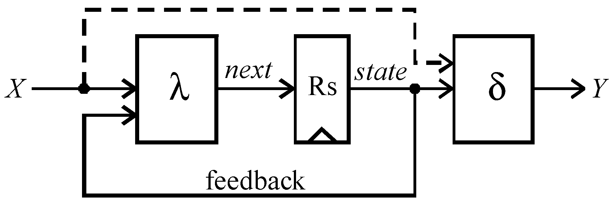
Figure 1 shows the traditional structure of an FSM, where X represents the input signals (input vector); Y represents the output signals (output vector); Rs is the state register storing the present-state code; λ is the combinational circuit (logic) determining the code of the next state (λ: X × SS); δ is the combinational circuit generating the values of the output signal; and S is the set of states of the FSM. The feedback loop connects the register Rs output to the input of the combinational circuit λ. For a Moore FSM, the output signal values are generated based on the present-state code (δ: SY), and for a Mealy FSM, based on the present-state code and the input signal values (δ: X × SY). Therefore, for a Mealy FSM, the X inputs are connected to the inputs of the combinational circuit λ (marked with a dotted line in Figure 1).
External disturbances can cause the following faults in the structure of an FSM:
  • At the inputs: an invalid input vector X;
  • In the state register Rs or in the feedback loop: an invalid code state of the present state;
  • In the logic λ: generation of an invalid code next for the next state;
  • In the logic δ or at the FSM outputs: generation of an invalid output vector Y.
Moreover, external disturbances can cause behavioral-level faults in the FSM, such as invalid transitions between legal states.
Designing fault-tolerant FSMs (FTFSMs) to eliminate external disturbances involves addressing the following tasks: fault detection (1), fault location (2), fault containment (3), and fault recovery (4). The robustness of an FSM can also be improved by using a special style of describing the FSM in hardware description language (HDL).
This paper presents a new method for designing FTFSMs that detects and eliminates multi-bit errors (MBUs) caused by external disturbances in the input and output vectors, in the present- and next-state codes, and neutralizes errors in the FSM behavior.
In the proposed approach, (1) fault detection is achieved by incorporating a concurrent error detection (CED) circuit into the FSM structure; fault location (2) is identified using specialized combinational circuits (logic) included within the CED circuit; (3) fault containment is accomplished using the output register Ro; and lastly, (4) fault recovery is implemented by controlling the clock enable (CE) input of the registers Rs and Ro, as well as by using the system processor.
This paper aims to develop robust FTFSMs for operation under MBUs caused by external disturbances, such as electromagnetic pulses and laser beams, resulting from EW.
The main contributions of this work are as follows:
  • Structural models of FTFSMs for detecting specific faults, a generalized FTFSM structure, and a CED circuit structure;
  • A method for synthesizing FTFSMs, which includes an algorithm for operating a CED circuit and an algorithm for synthesizing a generalized FTFSM structure;
  • Experimental studies demonstrating the effectiveness of the proposed approach when FTFSM states are encoded using one-hot and binary codes;
  • A technique for calculating the probability of fault detection when implementing an FTFSM in an FPGA using one-hot and binary state encoding;
  • Recommendations for the practical application of the proposed approach to designing robust FTFSMs.
The paper is organized as follows. Section 2 provides an overview of relevant work in this area. Section 3 outlines the key concepts and the method for designing FTFSMs. Section 4 presents the experimental results and their analysis, along with recommendations for the practical application of the discussed approach. A technique for calculating the fault detection probability in FTFSMs implemented in FPGAs is described in Section 5. Finally, Section 6 presents a summary of the paper.

2. Related Works

Digital devices such as FPGAs, SoCs, and ASICs are often subject to short- or long-term faults caused by external disturbances. These faults can affect both combinational and sequential logic: in the first case, the fault effect, called a single-event transient (SET), is a pulse on a signal that, if latched in a register, results in an erroneous value; in the second case, the fault, called a single-event upset (SEU), causes a state change in a memory cell. These types of faults are commonly referred to as soft errors, which can be recovered by overwriting the correct value. This paper discusses multi-bit soft errors.
First and foremost, it is crucial to detect any faults in the FSM. There are various approaches to fault detection in FSMs, including Hamming codes [3], immunological principles [4], a probabilistic detector [5] that analyzes discrepancies between observed and expected state-occupancy frequencies, convolutional codes [6], and selective partial replication [7].
Among fault-detection methods, CED techniques hold particular significance. CED circuits operate in parallel with the digital system, allowing for early fault detection. These circuits detect errors in FSMs by comparing the monitor outputs with the sequencer outputs [8], analyzing signatures [9], performing parity checks [10], and using Bose-Lynn codes [11]. In [12,13] for Moore FSMs and [14] for Mealy FSMs, the CED circuit for detecting MBUs is proposed. This circuit is designed to detect errors in both the input and output vectors, as well as in the present- and next-state codes. Additionally, it can detect invalid state transitions.
A common method for implementing fault-tolerant systems in very large-scale integration (VLSI) devices is known as triple modular redundancy (TMR) [15]. In TMR, the outputs from three identical replicas of logic units or registers are combined using a majority voting mechanism to generate a single output signal. If one of the three replicas fails, the other two can detect and correct the error, effectively masking the fault.
There are various methods for enhancing TMR in FSM designs. One approach, presented in [16], focuses on improving circuit resilience against SEUs by selectively applying TMR to sensitive subcircuits. Another method discussed in [17] suggests optimizing TMR logic by strategically placing voters. In [18], a place-and-route algorithm is considered that, in combination with TMR, mitigates the effects of SEU in FPGA configuration memory.
The double modular redundancy (DMR) method is an alternative to TMR and is commonly used in the design of FTFSMs. In [19], the DMR method is utilized to create FTFSMs within FPGA memory blocks. Reference [20] examines the reliability of FTFSMs that employ both DMR with self-checking and TMR methods. In [21], when implementing sequential circuits in ASICs, DMR architectures use self-checking asynchronous circuits to mitigate the effects of single-event transients (SETs).
Fault tolerance in FSMs can be achieved through various FSM state-encoding methods. Reference [22] discusses constant errors in the state register of an FSM and proposes a state-encoding algorithm designed for a specific number of errors. In [23], the states of an FTFSM are encoded using a k-of-n code, where each code word of length n contains exactly k ones. Reference [24] introduces separable codes, specifically Berger codes, which assign a vector of length k (where k = log2n) to an information vector of length n. This vector represents a binary number indicating the count of ones (or zeros) in the information vector. In [25], four methods for encoding the states of FTFSMs are compared: one-hot, binary, Hamming-2, and Hamming-3. The comparison reveals that while the Hamming-3 code offers the best fault tolerance, it requires the most resources and operates the slowest. On the other hand, the Hamming-2 code strikes an optimal balance between size, speed, and fault tolerance.
Some studies use HDLs, such as VHDL and Verilog, to design FTFSMs. In [26], a tool is introduced that synthesizes FTFSMs capable of handling SEUs in the state register. This tool automates the implementation of two FTFSM architectures, which can be specified in either KIS format [27] or VHDL. Fault tolerance is achieved through the use of single-error-correcting (SEC) codes. In [28], two styles for describing FTFSMs in Verilog, named safe0 and safe1, are presented. These styles are designed to prevent MBUs in both the input vector and the state register.
A significant number of studies have focused on the design of FTFSMs, characterized by a wide variety of approaches. In [29], a method for designing self-checking FSMs using Berger codes is explored. Reference [30] compares FTFSM architectures in terms of area and performance under SEUs. In [31], an approach to hardware fault tolerance is demonstrated using a fault-detection method inspired by the human immune system. In [32], redundant equivalent states are proposed for the design of FTFSMs to protect a small number of states with a high probability of SEU occurrence.
In [12], structural models of Moore FSMs are explored, focusing on fault detection and the mitigation of their effects on controlled objects. The structural models enable the identification of invalid transitions between FSM states, as well as invalid input and output vectors for each state and for the FSM as a whole. Furthermore, they can detect invalid codes for both the present and next states. Additionally, reference [12] provides area and performance estimates for these structural models. In [13], it is demonstrated that selecting an appropriate structure can prevent an increase in area and, in certain cases, even enhance the performance of FTFSMs. Reference [14] discusses structural models of Mealy FTFSMs aimed at fault detection. It presents combined structural models and identifies potential causes of faults that each FSM structural model can detect. Various styles for describing structural models of FTFSMs in Verilog HDL, including combined structural models, are presented in [33]. A methodology for constructing structural models of fault-tolerant Moore FSMs implemented on an FPGA is given in [34].
The main difference between the proposed approach to designing FTFSMs and existing methods is as follows. Most methods for designing FTFSMs (with the exceptions of [12,13,14,33,34]) consider single-event faults (SEUs), i.e., a single-bit change in the FSM state register. However, single-event faults (SETs), i.e., faults in the combinational circuits λ and δ, are rarely considered. Furthermore, faults in the input vector X are not considered, nor are behavioral-level faults that lead to invalid transitions between legal states. The proposed approach is free from these shortcomings. It involves the detection of multi-bit upsets (MBUs) of the SEU and SET types:
  • In the input vector X;
  • In the output vector Y;
  • In the state register Rs;
  • In the present- and next-state codes state and next.
Furthermore, the proposed approach enables the detection of FSM faults when an invalid transition occurs between legal states.
In the proposed approach, the synthesis of FTFSMs is performed at the structural level and at the level of the FSM description in a hardware description language (HDL). This paper uses Verilog as the HDL, but the proposed approach can easily be applied to VHDL and SystemVerilog.
Unlike the works in [12,13,14,33,34], this paper presents modified structural models of FTFSMs for specific fault detection, which enable the detection of faults in both Mealy FSMs and Moore FSMs; a new generalized structure for FTFSMs and CED circuits; new algorithms for synthesizing CED circuits and FTFSMs; and, for the first time, a technique for calculating the probability of fault detection when implementing FTFSMs in FPGAs.

3. Designing FTFSMs

3.1. Structural Models of FTFSMs

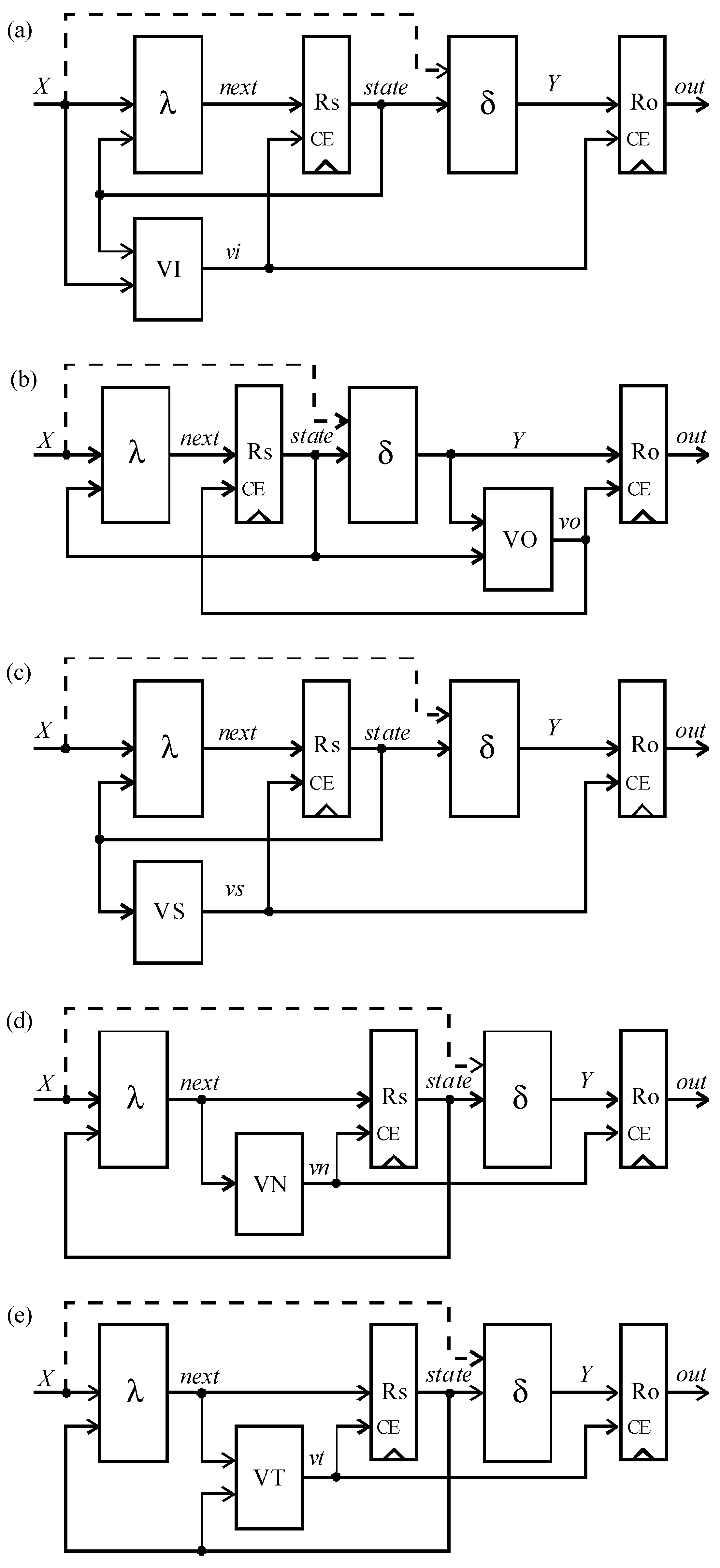
Structural models of FTFSMs that can detect faults caused by external disturbances are shown in Figure 2, where the VI structure defines a valid input vector, the VO structure defines a valid output vector, the VS structure defines a valid present-state code, the VN structure defines a valid next-state code, and the VT structure defines a valid transition between states.
The structures in Figure 2 include the additional output register Ro, which prevents faults from affecting the controlled object. Registers Rs and Ro have an extra input CE, to control register triggering. Each structure in Figure 2 includes a combinational circuit of the same name for fault detection. Combinational circuits VI, VO, VS, VN, and VT operate using inverse logic: the output signals vi, vo, vs, vn, and vt are set to 1 in the absence of a fault and to 0 in its presence.
The vi, vo, vs, vn, and vt signals control the CE input of the Rs and Ro registers. If a fault is detected, the CE inputs will be set to 0, preventing the registers from responding to the clock signal and causing the FSM to enter standby mode. In standby mode, the Rs register stores the code of the last present state, and the Ro register stores the value of the last output vector. Thus, in the event of a fault, the FSM remains in its last valid state, and the last valid output vector is stored at the FSM output. When the external disturbance ceases, and the CE inputs are set to 1, the FSM continues to operate in normal mode from the last valid state, i.e., without changing the control algorithm.
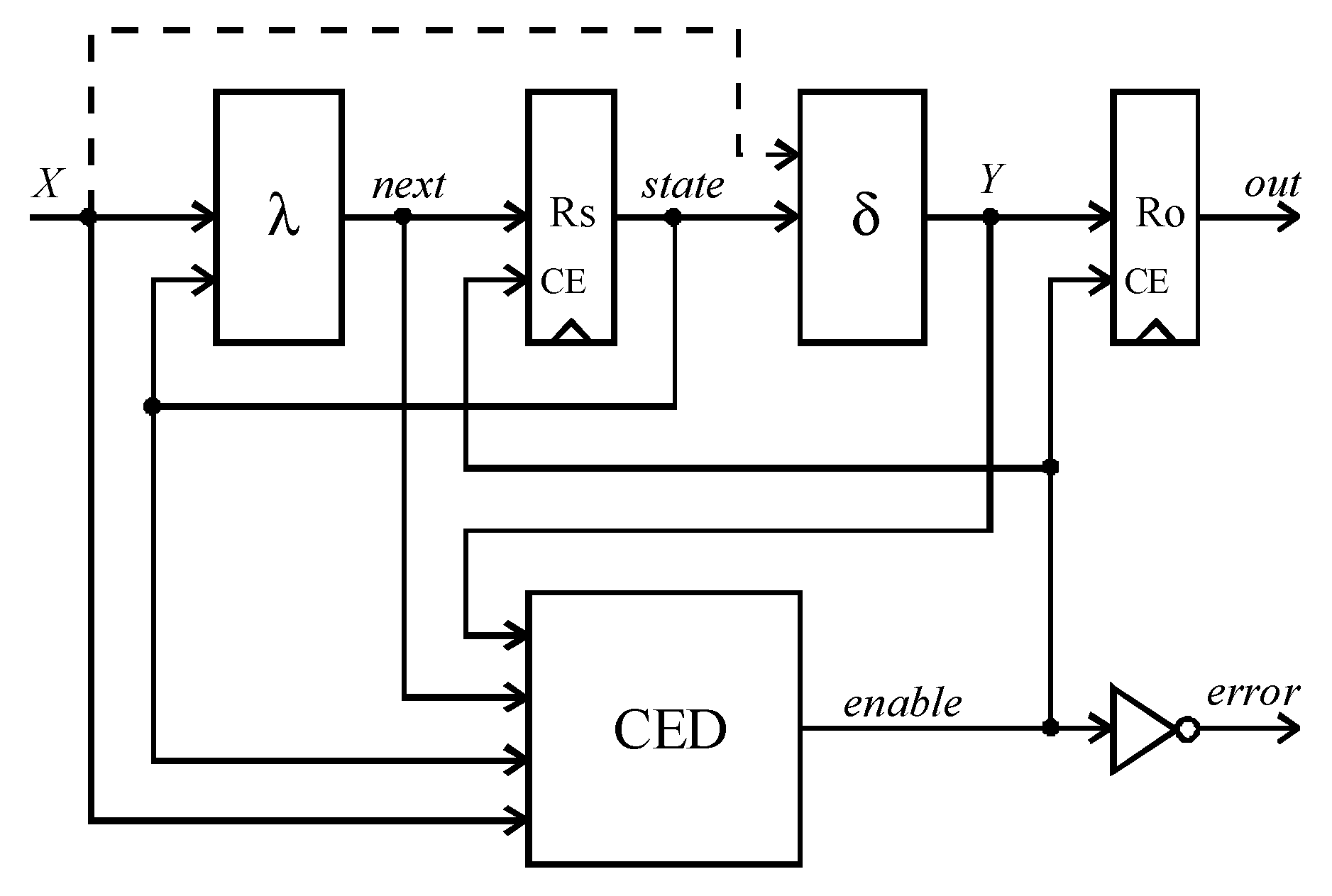
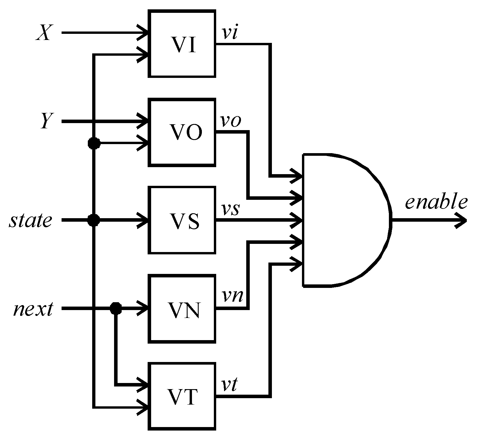
A generalized structure of the FTFSM is shown in Figure 3. To simultaneously detect multiple faults, the combinational circuits VI, VO, VS, VN, and VT can be combined into a single CED circuit. Depending on the types of faults to be detected, the CED circuit can include any subset of combinational circuits from the set {VI, VO, VS, VN, VT}. To detect all possible faults, the structure of the CED circuit is illustrated in Figure 4.
The output of the CED circuit is the signal enable, which controls the CE inputs of the registers Rs and Ro. The output signal enable of the CED circuit is determined using a logical “AND” operation that combines the vi, vo, vs, vn, and vt signals. Consequently, the enable signal will be a logical ‘0’ if a fault is detected, and a logical ‘1’ otherwise.
The FTFSM shown in Figure 3 also includes an additional output error for error reporting, which is the inverse of the signal enable. The signal error informs the external environment about a problem, prompting further action to correct the fault. For example, if an FTFSM implemented in an FPGA does not return to normal operation for a long time, a decision may be made to reconfigure the FPGA or the part of the FPGA that contains the FTFSM.
Note that the output register Ro in the structure of an FTFSM eliminates short-term pulses (glitches) at the outputs of Mealy-type FSMs, which arise from their asynchronous nature with respect to the inputs.

3.2. Synthesis of FTFSMs

Let K be the set of state codes of an FSM; X(si) be the set of input vectors that initiate transitions from state si; Y(si) be the set of output vectors that are formed during transitions from state si; and S(si) be the set of states in which transitions from state si end, siS.
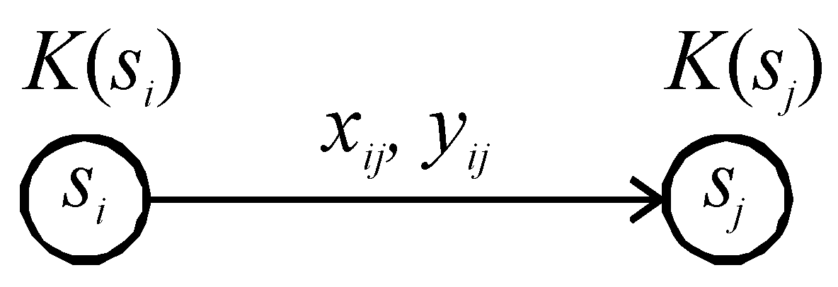
Figure 5 shows the transition between two states of an FSM, where si is the initial state of the transition, siS; sj is the final state of the transition, sjS(si); K(si) is the code of the state of si; K(sj) is the code of the state of sj, K(si), K(sj) ∈ K; xij is the input vector initiating the transition between states si and sj, xijX(si); and yij is the output vector formed by the FSM during the transition between states si and sj, yijY(si). Note that the code K(si) corresponds to the variable state, and the code K(sj) corresponds to the variable next in Figure 2 and Figure 3.
The combinational circuit VI checks the correctness of the input vector at state si using expression (1):
v i = 1 , x i j X s i ; 0 , x i j X s i ;
where the signal vi = 1 if the input vector xij is valid in state si, i.e., initiates some transition from state si; otherwise, vi = 0.
The combinational circuit VO checks the validity of the output vector in state si using expression (2):
v o = 1 , y i j Y s i ; 0 , y i j Y s i ;
where the signal vo = 1 if the output vector yij is valid in state si, i.e., formed during some transition from state si; otherwise, vo = 0.
The combinational circuit VS checks the validity of the present-state code K(si) using expression (3):
v s = 1 , K ( s i ) K ; 0 , K ( s i ) K ;
where the signal vs = 1 if the code K(si) is valid, i.e., is one of the state codes of the FSM; otherwise, vs = 0.
Similarly, the combinational circuit VN checks the validity of the code of the next state K(sj) using expression (4):
v n = 1 , K ( s j ) K ; 0 , K ( s j ) K ;
where the signal vn = 1 if the code K(sj) is valid, i.e., is one of the state codes of the FSM; otherwise, vn = 0.
The set of all transitions of the FSM can be defined as the set T of pairs (si, sj) as follows:
T = s i , s j s i S , s j S ( s i ) } .
The combinational circuit VT checks the validity of the transition between states si and sj using expression (6):
v t = 1 , s i , s j T ; 0 , s i , s j T ;
where the signal vt = 1 if the transition from state si to state sj is valid; otherwise, vt = 0.
Based on expressions (1)–(6), the functioning of the CED circuit can be described using Algorithm 1.
Algorithm 1: Functioning of the CED circuit
INPUT: xij, yij, K, K(si), K(sj), T.
OUTPUT: enable.
Definition of sets: X(si), Y(sj), S(si).
if xijX(si)         then vi = 1;
                                          else vi = 0;
if yijY(si)          then vo = 1;
                                          else vo = 0;
if K(si) ∈ K           then vs = 1;
                                          else vs = 0;
if K(sj) ∈ K           then vn = 1;
                                          else vn = 0;
if (si, sj) ∈ T         then vt = 1;
                                          else vt = 0;
enable = vi & vo & vs & vn & vt;
Return enable.
The process of synthesizing FTFSMs is represented in Algorithm 2.
Algorithm 2: Synthesis of FTFSMs
  • The types of faults to be detected are defined (input vector, output vector, present-state code, next-state code, state transitions).
  • Based on the fault types defined in Step 1, the structure of the CED circuit in Figure 4 is determined (a subset of combinational circuits from the set {VI, VO, VS, VN, VT}).
  • In accordance with Algorithm 1, the CED circuit is synthesized.
  • The description of the FTFSM is generated in one of the HDLs.
  • End.
The robustness of the CED circuit is ensured by its small area relative to the FSM. Therefore, the CED circuit (Step 2 of Algorithm 2) should include only those combinational circuits that detect the most likely faults.
To describe FTFSMs in one of the HDLs, the robust_0 style [33] is used, which improves FSM robustness. In this style, undefined transitions are redefined to transition to the initial state of the transition, i.e., the FSM does not change its state, and the outputs for undefined transitions are redefined as the zero vector.

3.3. Example of Designing the FTFSM

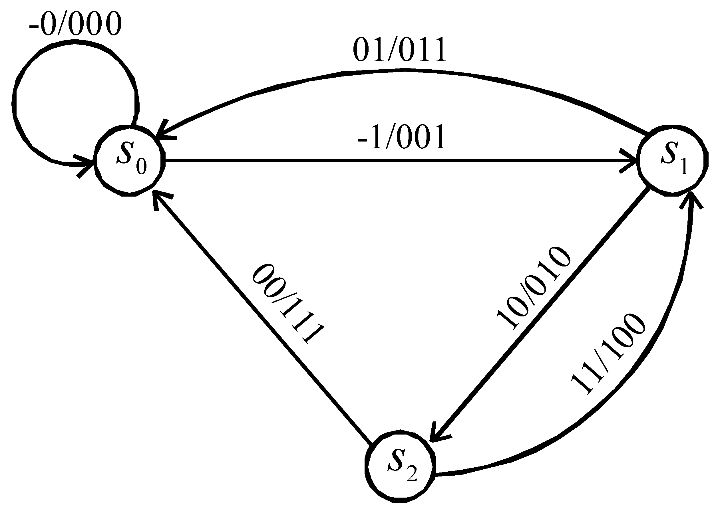
It is necessary to construct an FTFSM described by the state transition graph (STG) shown in Figure 6.
In Figure 6, the STG vertices represent the states of the FSM, and the STG arcs correspond to the transitions between states. Near each arc, the input vector that initiates the transition is indicated, followed by a slash that separates it from the output vector generated by the FSM during this transition. A hyphen in an input or output vector denotes a “don’t care” value. Our FSM has three states, two inputs, and three outputs.
Let it be necessary to construct an FTFSM that detects all the faults under consideration. In this case, the structure of the CED circuit corresponds to the structure shown in Figure 4. The sets X(si), Y(si), and S(si) for our FSM, generated according to Algorithm 1, are presented in Table 1.
After the sets X(si), Y(sj), and S(si) are formed in accordance with Step 4 of Algorithm 2, the description for the FTFSM is created using one of the HDLs. An example of an FTFSM description in Verilog HDL is given in Appendix A.

4. Experimental Research

The efficiency of the considered approach for synthesizing FTFSMs was investigated using the FSM benchmarks developed by the MCNC [35]. The FSMs were implemented on Cyclone 10 LP FPGAs using the Altera Quartus Prime version 25.1 design tool. The area of the FSMs was measured by determining the number of look-up tables (LUTs) used, while the performance was defined as the maximum operating frequency of the FSM circuit. The FSM states were encoded using binary and one-hot codes. The FTFSMs were constructed according to the structure shown in Figure 3 and Figure 4, when the CED circuit includes all combinational circuits from the set {VI, VO, VS, VN, VT}.
These experimental studies aim to evaluate the increase in area and decrease in performance of FTFSMs compared to traditional FSM implementations, where the FSM is described in Verilog HDL using a three-process style [36].

4.1. Area of FTFSMs

An increase in the area of FTFSMs is expected compared to traditional FSM implementations for several reasons. The structure of an FTFSM (Figure 3) includes an additional output register Ro, a CED circuit, and an inverter that generates the signal error. In addition, the number of FTFSM outputs has been increased by 1 for the signal error, compared to the traditional FSM structure (Figure 1). Therefore, the following hypothesis can be put forward.
Hypothesis 1.
The average area of FTFSMs is larger than that of traditional FSMs.
Table 2 presents the results of a study comparing the area of FTFSMs with that of traditional FSM implementations and the TMR method. The variables Ltb, Lto, and Ltmrb represent the areas of traditional FSMs with binary and one-hot state encoding, respectively, as well as the TMR method with binary state encoding. In contrast, Lfb and Lfo indicate the area of FTFSMs with binary and one-hot state encoding, respectively. The ratios Lfb/Ltb, Lfo/Lto, and Ltmrb/Lfb reflect the comparison of the corresponding parameters. Additionally, the variables Av, Min, and Max denote the arithmetic mean, minimum, and maximum values of the analyzed parameters.
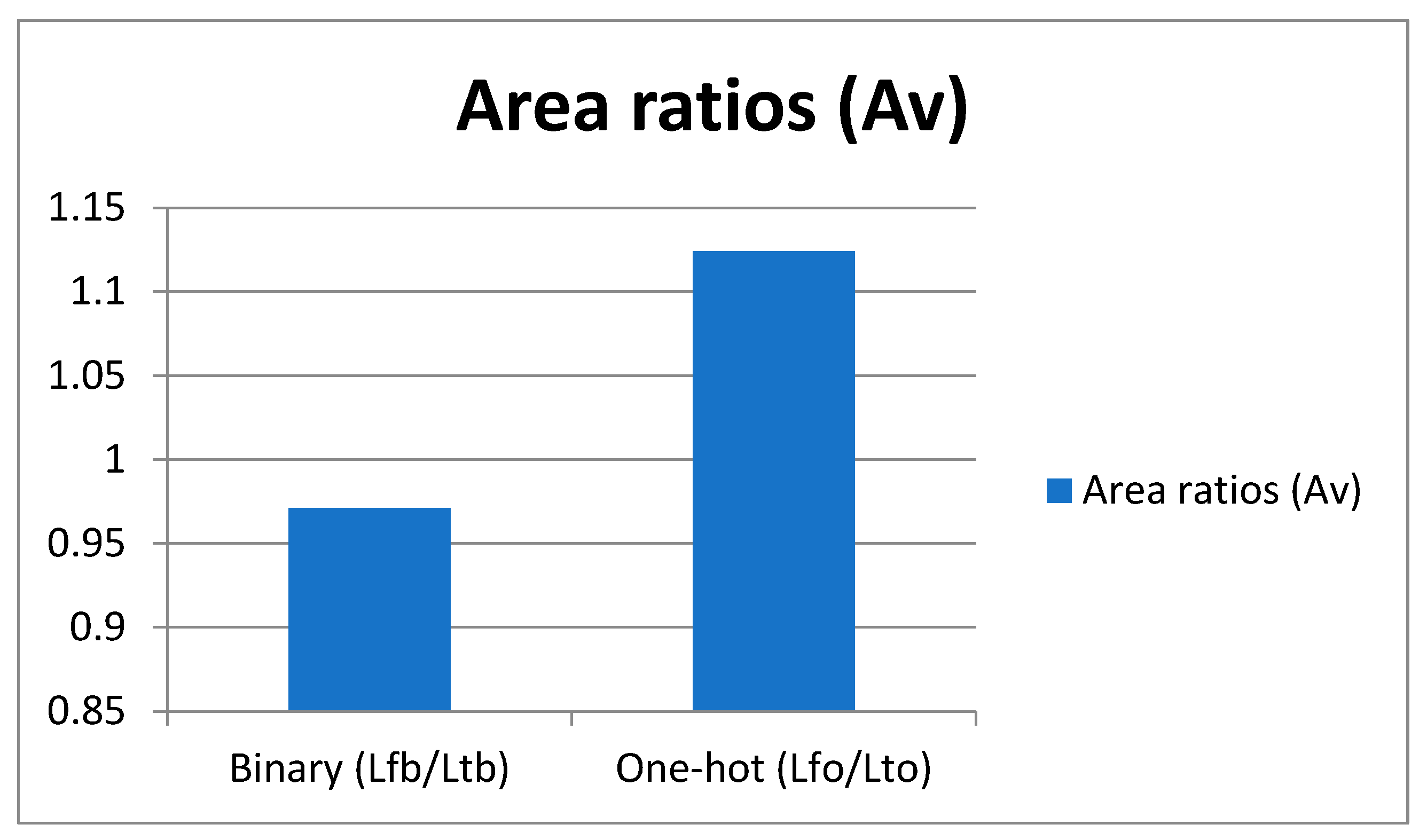
When using binary codes to perform FSM state encoding, as shown in Table 2, there is a maximum increase in area by a factor of 3.071 for the example s208 and a maximum decrease in area by a factor of 6.1 (=1/0.165) for the example cse; meanwhile, on average the area does not increase, but rather, decreases by 2.9% (this corresponds to an Lfb/Ltb ratio of 0.971).
The reduction in the area of FTFSMs compared to traditional FSM implementations is explained by the use of the robust_0 style [33] to describe them. In the case of undefined FSM transitions, this style prevents the design tool from automatically installing latches in the FSM circuit to hold the FSM in the initial state of the transition and preserve the FSM output values.
When using one-hot encoding, the maximum area increases by a factor of 1.952 for the s832 example, and the maximum area decreases by a factor of 1.727 (=1/0.579) for the train4 example. On average, the area increases by 12.4%, corresponding to an Lfo/Lto ratio of 1.124.
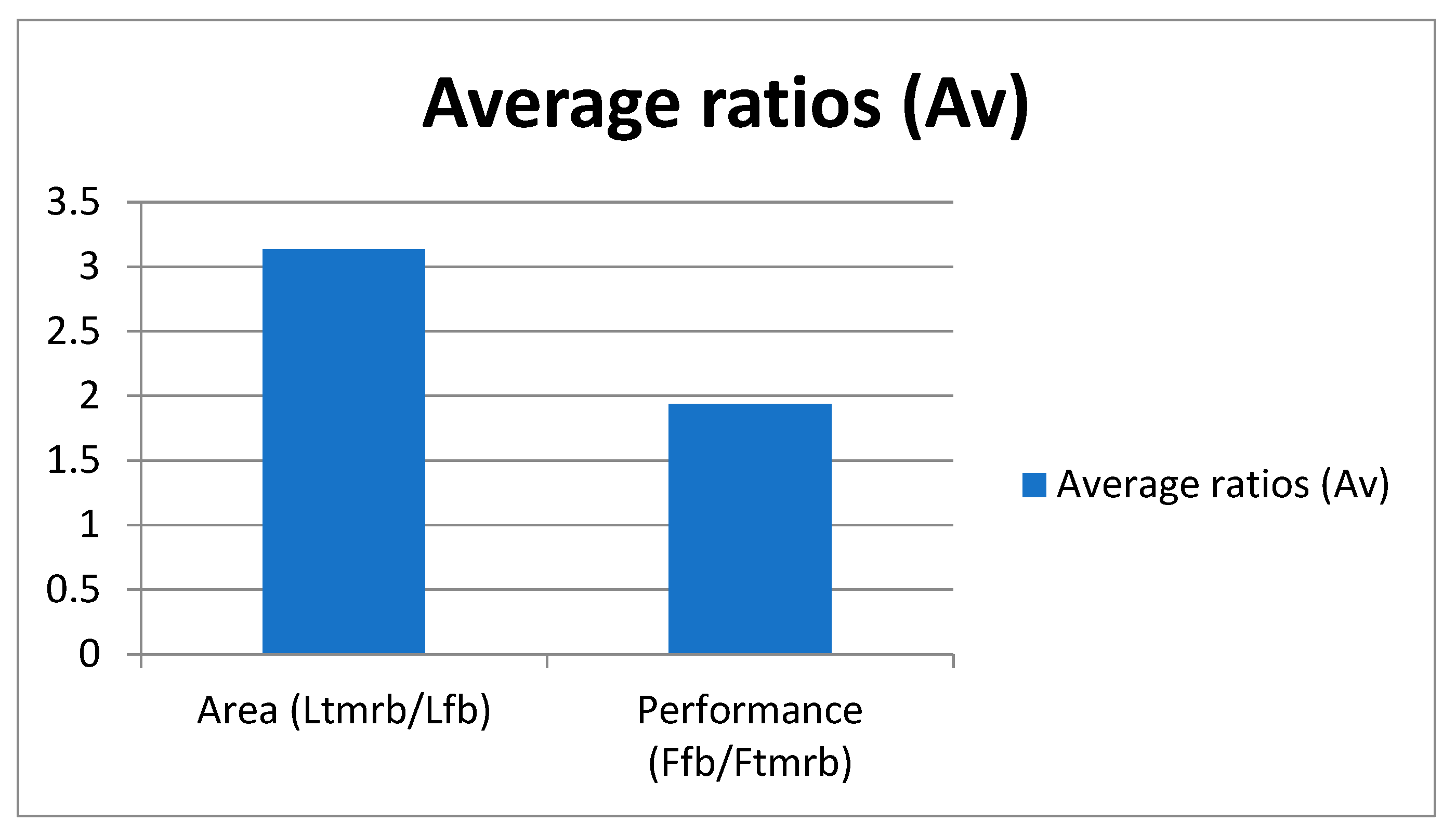
Compared to the TMR method, the proposed approach reduces the average area of FTFSMs by a factor of 3.137 (and by more than 8 times in the cse example).
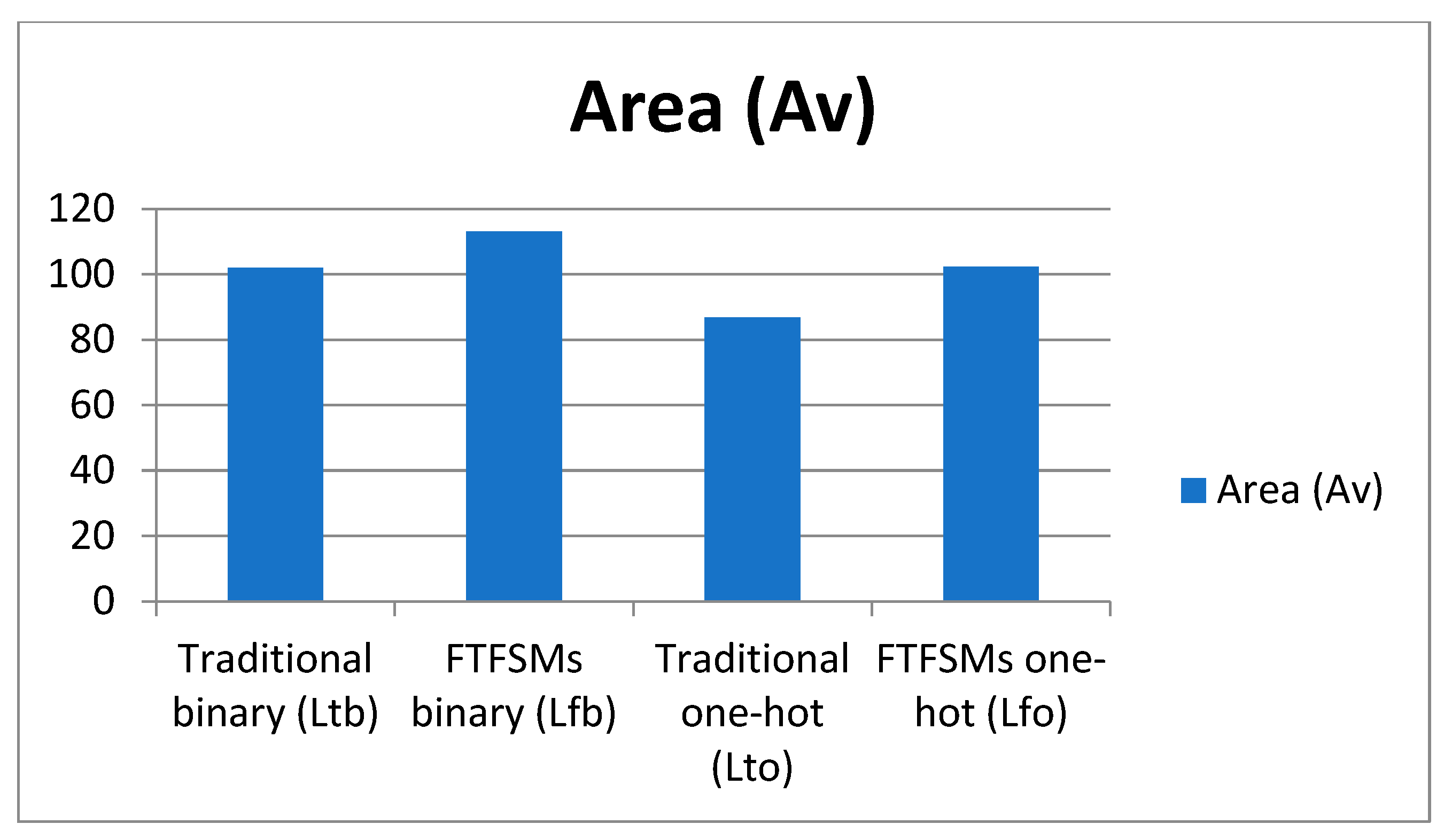
The ratios of the average area values for the traditional implementation of FSMs and for the proposed FTFSM synthesis method, when using binary and one-hot state encodings, are shown in Figure 7. However, when comparing the average area values (rather than the ratios) in Figure 8, it can be seen that the proposed method increases the area by approximately 11% for binary encoding and by 18% for one-hot encoding.

4.2. Performance of FTFSMs

A decrease in the average performance of FTFSMs can be expected compared to traditional FSM implementations, since the structure of an FTFSM additionally includes the output register Ro and the CED circuit. Therefore, the following hypothesis can be put forward.
Hypothesis 2.
The average performance of FTFSMs is lower than that of traditional FSMs.
Table 3 presents the results of a study of the performance of FTFSMs in comparison with traditional FSM implementations, where Ftb, Fto and Ftmrb are the performance (in MHz) of traditional FSMs with binary and one-hot state encoding, as well as the TMR method with binary state encoding; Ffb and Ffo are the performance of FTFSMs when using binary and one-hot codes for encoding states; Ftb/Ffb, Fto/Ffo and Ffb/Ftmr are the ratios of the corresponding parameters; and Av, Min, and Max denote the previous values.
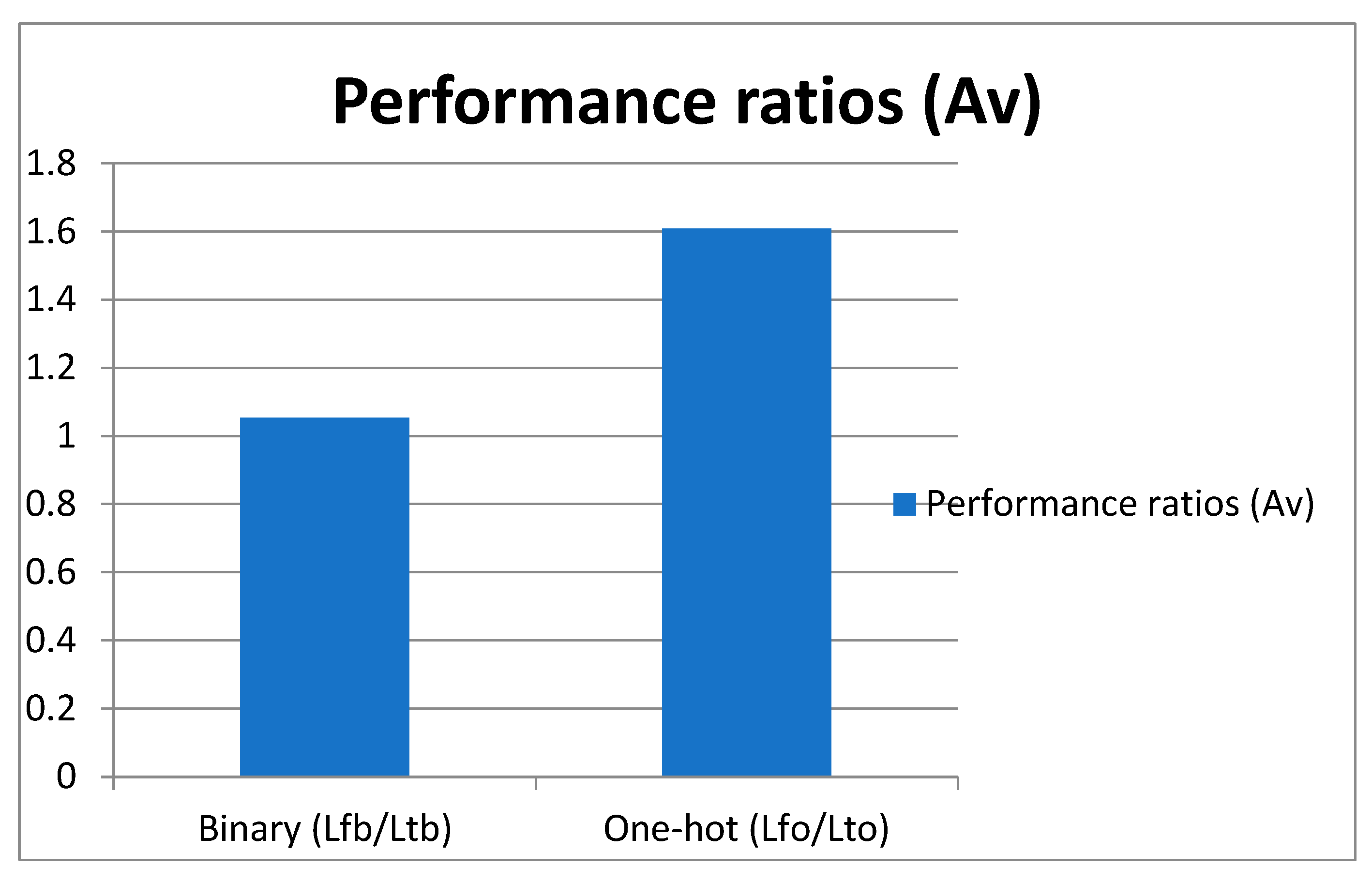
When using binary codes for FSM state encoding, as shown in Table 3, there is a maximum performance reduction by a factor of 1.912 for the example s820, a maximum performance increase by a factor of 3.523 (=1/0.284) for the example train4, and an average performance reduction of 5.3% (corresponding to a ratio of Ftb/Ffb = 1.053).
When using one-hot codes for FSM state encoding, the maximum performance reduces by a factor of 3.390 for the example planet, the maximum performance increases by a factor of 1.932 (=1/0.518) for the example train4, and the average performance reduces by 60.9% (corresponding to a ratio Ftb/Ffb = 1.609).
Compared to the TMR method, the proposed approach increases the average performance of FTFSMs by a factor of 1.939 (up to 4.5 times for the s420 example).
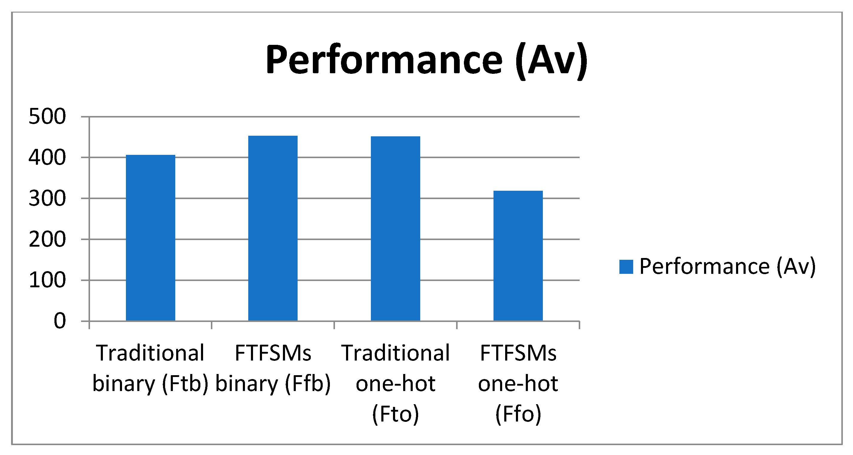
The performance ratios for traditional FSM implementations and for the proposed FTFSM synthesis method, using binary and one-hot state encodings, are shown in Figure 9. However, the comparison of the average performance values (not the ratios) in Figure 10 shows that using the proposed approach increases performance by 11.6% when using binary encoding, but reduces performance by 41.8% when using one-hot encoding.
The performance increase in FSMs, in some cases, compared to traditional FSMs, is explained by the fact that a decrease in the area of the combinational part often leads to improved performance.
In summary, Hypothesis 1 was confirmed for the one-hot FSM state encoding and not confirmed for the binary FSM state encoding. Hypothesis 2 was also confirmed for the one-hot FSM state encoding and not confirmed for the binary FSM state encoding.
Figure 11 shows, on average, by how many times the proposed approach reduces the area and increases the performance of FTFSMs compared to the TMR method (the average area and performance ratios).
Based on the experimental results, we recommend using minimum-length codes, such as binary or Gray codes, for encoding the states of FTFSMs. In this approach, the performance of FTFSMs is only slightly reduced compared to traditional FSM implementations, while the area requirements increase only marginally or may even decrease.

5. Fault Detection Probability When Implementing FTFSMs in FPGAs

When implementing an FSM in an FPGA, faults can occur not only in the FSM wires and registers but also in the configuration memory cells that define the FSM circuit. These faults can lead to failures in the combinational circuits of the FTFSM (λ, δ, VI, VO, VS, VN, VT, and CED), as well as in the Rs and Ro registers. The task is to calculate the probability of detecting faults in the FTFSM shown in Figure 3, while accounting for faults in the CED circuit.
The probability of a fault occurring in a specific component of an FSM implemented in an FPGA depends on the area of the crystal occupied by that component. Note that for FPGAs based on LUTs, the component area is determined by the number of LUTs required to implement this component. The probability of a fault occurring in a component e, e ∈ {λ, δ, Rs, Ro, CED}, can be calculated using expression (7):
p e = A e A F S M ,
where Ae and AFSM represent the area of the component e and the area of the FSM, respectively.
Since the probabilities of a fault occurring in each component of the FSM are independent, condition (8) must be satisfied:
p λ + p δ + p R s + p R o + p C E D = 1 .
The probability of detecting a fault in any component of an FSM e, where e ∈ {λ, δ, Rs, Ro}, in the absence of a fault in the combinational circuit CED, is determined by expression (9):
b e = p e · q C E D ,
where qCED represents the probability of no faults in the combinational circuit CED:
q CED = 1 p CED .
By analogy with (9), the probability pd of detecting a fault in any component of the FTFSM in Figure 3 in the absence of a fault in the combinational circuit CED is determined by expression (11):
p d = p λ + p δ + p R s + p R o · q C E D .
Considering expression (8), we have:
p d = ( 1 p C E D ) · q C E D ,
and also taking into account (10), we obtain:
p d = q C E D · q C E D = q C E D 2 .
Thus, the probability pd of detecting a fault in the FTFSM, according to (7), (10) and (13), depends on the area of the combinational CED circuit. When implementing an FTFSM in an LUT-based FPGA, the area of the combinational circuit CED, according to [37], is determined by the number of LUTs using expression (14):
A C E D = 1 , r a n k C E D n ; r a n k C E D n n 1 , r a n k C E D > n ;
where rank(CED) is the number of inputs of the combinational circuit CED; n is the number of LUT inputs; and ⌈A⌉ is the smallest integer greater than or equal to A.
From Figure 2 and Figure 3, it follows that the ranks (number of inputs) of combinational circuits of an FTFSM are determined by the following expressions (15):
r a n k V I = X + C ; r a n k V O = X + Y ; r a n k V S = r a n k V N = C ; r a n k V T = 2 · C ; r a n k C E D = X + Y + 2 · C ;
where |A| is the cardinality of set A, and C is the length (number of bits) of the FSM state codes.
When using binary encoding, the length Cb of FSM state codes is equal to
C b = log 2 S ,
and when using one-hot encoding, the length Co of FSM state codes is equal to
C o = S .
The probability calculation for detecting a fault in an FTFSM implemented on an FPGA is represented by Algorithm 3.
Algorithm 3: Calculating the probability of fault detection for FTFSMs in an FPGA
INPUT: The FTFSM.
OUTPUT: pd.
  • The code length C is determined based on the method of encoding the FTFSM states, for example, as specified in (16) or (17).
  • According to (15), the rank of the circuit CED for fault detection is determined.
  • According to (14), the area of the circuit CED is determined.
  • In accordance with Algorithm 2, the synthesis of an FTFSM is performed, and the area AFSM of the FTFSM is determined.
  • According to (7), the probability pe of fault of the CED circuit is calculated.
  • According to (10), the probability qCED of the absence of a fault in the CED circuit is calculated.
  • According to (13), the probability pd of detecting a fault by the CED circuit is calculated.
Return pd.
As an example, let us determine the probability of detecting faults using the proposed technique, based on the average parameter values of FSM benchmarks [35], for which |X| = 6, |Y| = 6, and |S| = 22. Note that for the Cyclone 10 LP family of FPGAs, the number of LUT inputs, n, is 4.
Let us calculate the probability of detecting faults when using binary codes for encoding the FSM states. From (16) it follows that for |S| = 22, the code length Cb = 5. The average value Lfb = 113.14 from Table 2 is considered to be the area AFSM of the FTFSM.
Let us consider the cases when the CED circuit consists of only one combinational circuit e, e ∈ {VI, VO, VS, VN, VT}, and also when the CED circuit includes all combinational circuits, as shown in Figure 4. The results of executing Algorithm 3 are given in Table 4, where the probability of detecting faults as a percentage is added.
When using one-hot codes for FSM state encoding, according to (17), C o = S = 22, and the area AFSM of the FSM is taken to be the average value of the area Lfo = 102.33 of the FTFSMs from Table 2. The results of executing Algorithm 3 are given in Table 5.
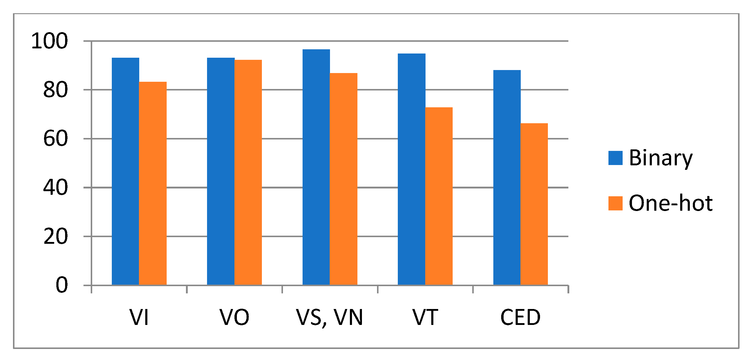
Figure 12 shows a comparison of the probabilities (in percent) of fault detection in FTFSMs using binary and one-hot encoding for various combinational circuits from the set {VI, VO, VS, VN, VT}, and also when the CED circuit includes all combinational circuits.
Table 4 and Table 5, as well as Figure 12, show that, with binary encoding, the fault-detection probability for FTFSMs implemented in FPGAs ranges from 93.1 to 96.5% for various faults and 88.0% for all faults. Using one-hot encoding, the fault-detection probability ranges from 72.8 to 92.3% for individual faults and 66.3% for all faults. Therefore, to increase the fault-detection probability in FTFSMs implemented in FPGAs, the FTFSM states should be encoded with minimal-length codes, such as binary or Gray.

6. Conclusions

This paper introduces a method for creating robust FTFSMs that can detect MBUs caused by external disturbances from EW systems affecting UAVs. The FTFSM structure is designed to identify faults in the input and output vectors, as well as in the present- and next-state codes, and it can detect invalid state transitions. When a fault is detected, the FTFSM enters a standby mode, during which it saves the code of the last present state and the value of the last valid output vector. Once the external disturbance ceases, the FTFSM returns to normal operation without changing the control algorithm. In the case of a critical error, the FTFSM circuit can be reconfigured using an external processor. Experimental studies have shown the high efficiency of this proposed approach. For example, compared with traditional FSM implementations that use one-hot state encoding, the area required for FTFSMs is reduced by an average of 2.9%, while performance decreases by an average of 5.3%. Furthermore, compared to the TMR method, the proposed approach reduces the average area by a factor of 3.137 and improves average performance by a factor of 1.939. Additionally, a technique for calculating the probability of fault detection when implementing FTFSMs on FPGAs is presented. To minimize overhead and increase the probability of fault detection, it is recommended to use minimum-length codes, such as binary or Gray codes, to encode the FTFSM states. Future research will concentrate on developing methods for designing even more fault-tolerant and robust FSMs.

Funding

The research was carried out within project no. WZ/WI-IIT/5/2026 at Bialystok University of Technology and financed by a research subsidy from Bialystok University of Technology.

Institutional Review Board Statement

Not applicable.

Informed Consent Statement

Not applicable.

Data Availability Statement

The data supporting the findings of this study are derived from FSM benchmarks provided by the Microelectronics Center of North Carolina (MCNC). These benchmarks are openly accessible, with references and links included within the article.

Conflicts of Interest

The author declares no conflicts of interest.

Appendix A

module Mealy_FTFSM (
     input clk, reset,               // FSM ports
     input [1:0] x,
     output error,
     output reg [2:0] out);
 
     reg[1:0] state, next;       // state variables
 
     reg[2:0] y;                       // outputs generated by the machine
     wire enable;                   // enable signal for register switching
     reg vi, vo, vs, vn, vt;      // outputs of the logics VI, VO, VS, VN, and VT
 
     localparam [1:0]             // description of the states
          s0 = 0,
          s1 = 1,
          s2 = 2;
 
     always @(posedge clk, negedge reset)  // description of the Rs status register
          if (~reset)             state <= s0;           // reset
          else if (enable)    state <= next;        // transition to the next state
          else                       state <= state;       // saving the previous state
 
     always @(posedge clk, negedge reset) // description of output register Ro
          if (~reset)            out <= 0;                // reset
          else if (enable)   out <= y;                // forming a new output value
          else                     out <= out;             // keep the previous output value
 
     always @(*)         // description of transitions
          case(state)
          s0: casex(x)
                     2′b?0:   next = s0;
                     2′b?1:   next = s1;
                     default: next = s0;
                endcase
          s1: casex(x)
                     2′b01:   next = s0;
                     2′b10:   next = s2;
                     default: next = s1;
                endcase
          s2: casex(x)
                     2′b00:   next = s0;
                     2′b11:   next = s1;
                     default: next = s2;
                endcase
                default: next = s0;
          endcase
 
   always @(*)         // description of outputs
          case(state)
          s0: casex(x)
                     2′b?0:   y = 3′b000;
                     2′b?1:   y = 3′b001;
                     default: y = 3′b000;
                endcase
          s1: casex(x)
                     2′b01:   y = 3′b011;
                     2′b10:   y = 3′b010;
                     default: y = 3′b000;
                endcase
          s2: casex(x)
                     2′b00:   y = 3′b111;
                     2′b11:   y = 3′b100;
                     default: y = 3′b000;
                endcase
                default: y = 3′b000;
          endcase
 
   always @(*)         // VI logic description
          case(state)
          s0: casex(x)
                     2′b?0:   vi = 1′b1;
                     2′b?1:   vi = 1′b1;
                     default: vi = 1′b0;
                endcase
          s1: casex(x)
                     2′b01:   vi = 1′b1;
                     2′b10:   vi = 1′b1;
                     default: vi = 1′b0;
                endcase
          s2: casex(x)
                     2′b00:   vi = 1′b1;
                     2′b11:   vi = 1′b1;
                     default: vi = 1′b0;
                endcase
          endcase
 
   always @(*)         // VO logic description
          case(state)
               s0: case(y)
                     3′b000:   vo = 1′b1;
                     3′b001:   vo = 1′b1;
                     default:  vo = 1′b0;
               endcase
               s1: case(y)
                     3′b011:   vo = 1′b1;
                     3′b010:   vo = 1′b1;
                     default:  vo = 1′b0;
               endcase
               s2: case(y)
                     3′b111:   vo = 1′b1;
                     3′b100:   vo = 1′b1;
                     default:  vo = 1′b0;
              endcase
          endcase
 
     always @(*)         // VS logic description
          case(state)
               s0:    vs = 1′b1;
               s1:    vs = 1′b1;
               s2:    vs = 1′b1;
               default:  vs = 1′b0;
          endcase
 
     always @(*)         // VN logic description
          case(next)
               s0:    vn = 1′b1;
               s1:    vn = 1′b1;
               s2:    vn = 1′b1;
               default:  vn = 1′b0;
          endcase
 
     always @(*)         // VT logic description
          case(state)
               s0: case(next)
                     s0:   vt = 1′b1;
                     s1:   vt = 1′b1;
                     default: vt = 1′b0;
               endcase
               s1: case(next)
                     s0:   vt = 1′b1;
                     s2:   vt = 1′b1;
                     default: vt = 1′b0;
               endcase
               s2: case(next)
                     s0:   vt = 1′b1;
                     s1:   vt = 1′b1;
                     default: vt = 1′b0;
               endcase
               default:  vt = 1′b0;
          endcase
 
     // generation of the enable and error signals
     assign enable = vi & vo & vs & vn & vt;
     assign error = !enable;
endmodule

References

  1. Zhou, K.; Ren, Z. A new controller architecture for high performance, robust, and fault-tolerant control. IEEE Trans. Autom. Control 2001, 6, 1613–1618. [Google Scholar] [CrossRef]
  2. Yu, A.; Kolotylo, I.; Hashim, H.A.; Eltoukhy, A.E. Electronic warfare cyberattacks, countermeasures and modern defensive strategies of UAV avionics: A survey. IEEE Access 2025, 13, 68660–68681. [Google Scholar] [CrossRef]
  3. Hamming, R.W. Error detecting and error correcting codes. Bell Syst. Tech. J. 1950, 29, 147–160. [Google Scholar] [CrossRef]
  4. Bradley, D.; Tyrrell, A. A hardware immune system for benchmark state machine error detection. In Proceedings of the 2002 Congress on Evolutionary Computation, Honolulu, HI, USA, 12–17 May 2002. [Google Scholar] [CrossRef]
  5. Hadjicostis, C.N. Probabilistic detection of FSM single state-transition faults based on state occupancy measurements. IEEE Trans. Autom. Control 2005, 50, 2078–2083. [Google Scholar] [CrossRef]
  6. Rokas, K.; Makris, Y.; Gizopoulos, D. Low cost convolutional code based concurrent error detection in FSMs. In Proceedings of the 18th IEEE Symposium on Defect and Fault Tolerance in VLSI Systems, Boston, MA, USA, 5 November 2003. [Google Scholar] [CrossRef]
  7. Drineas, P.; Makris, Y. SPaRe: Selective partial replication for concurrent fault-detection in FSMs. IEEE Trans. Instrum. Meas. 2003, 52, 1729–1737. [Google Scholar] [CrossRef]
  8. Iyengar, V.S.; Kinney, L.L. Concurrent fault detection in microprogrammed control units. IEEE Trans. Comput. 1985, 100, 810–821. [Google Scholar] [CrossRef]
  9. Leveugle, R.; Saucier, G. Optimized synthesis of concurrently checked controllers. IEEE Trans. Comput. 1990, 39, 419–425. [Google Scholar] [CrossRef]
  10. Zeng, C.; Saxena, N.; McCluskey, E.J. Finite state machine synthesis with concurrent error detection. In Proceedings of the International Test Conference, Atlantic City, NJ, USA, 30 September 1999; pp. 672–679. [Google Scholar] [CrossRef]
  11. Das, D.; Touba, N.A. Synthesis of circuits with low-cost concurrent error detection based on Bose-Lin codes. J. Electron. Test. 1999, 15, 145–155. [Google Scholar] [CrossRef]
  12. Salauyou, V. Fault detection of Moore finite state machines by structural models. In Proceedings of the International Conference on Computer Information Systems and Industrial Management, Tokyo, Japan, 22–24 September 2023. [Google Scholar] [CrossRef]
  13. Solov’ev, V.V. Structural models for failure detection of Moore finite-state machines. J. Comput. Syst. Sci. Int. 2023, 62, 977–990. [Google Scholar] [CrossRef]
  14. Salauyou, V. Structural models of Mealy finite state machines detecting faults in control systems. Radioelectron. Comput. Syst. 2023, 3, 173–186. [Google Scholar] [CrossRef]
  15. Lyons, R.E.; Vanderkulk, W. The use of triple-modular redundancy to improve computer reliability. IBM J. Res. Dev. 1962, 6, 200–209. [Google Scholar] [CrossRef]
  16. Samudrala, P.K.; Ramos, J.; Katkoori, S. Selective triple modular redundancy (STMR) based single-event upset (SEU) tolerant synthesis for FPGAs. IEEE Trans. Nucl. Sci. 2004, 51, 2957–2969. [Google Scholar] [CrossRef]
  17. Kastensmidt, F.L.; Sterpone, L.; Carro, L.; Reorda, M.S. On the optimal design of triple modular redundancy logic for SRAM-based FPGAs. In Proceedings of the Design, Automation and Test in Europe, Munich, Germany, 7–11 March 2005. [Google Scholar] [CrossRef]
  18. Sterpone, L.; Violante, M. A new reliability-oriented place and route algorithm for SRAM-based FPGAs. IEEE Trans. Comput. 2006, 55, 732–744. [Google Scholar] [CrossRef]
  19. Tiwari, A.; Tomko, K.A. Enhanced reliability of finite-state machines in FPGA through efficient fault detection and correction. IEEE Trans. Reliab. 2005, 54, 459–467. [Google Scholar] [CrossRef]
  20. Cassel, M.; Lima, F. Evaluating one-hot encoding finite state machines for SEU reliability in SRAM-based FPGAs. In Proceedings of the 12th IEEE International On-Line Testing Symposium (IOLTS’06), Lake Como, Italy, 10–12 July 2006. [Google Scholar] [CrossRef]
  21. Teifel, J. Self-voting dual-modular-redundancy circuits for single-event-transient mitigation. IEEE Trans. Nucl. Sci. 2009, 55, 3435–3439. [Google Scholar] [CrossRef]
  22. Meyer, J.F. Fault tolerant sequential machines. IEEE Trans. Comput. 1971, C-20, 1167–1177. [Google Scholar] [CrossRef]
  23. Tohma, Y.; Ohyama, Y.; Sakai, R. Realization of fail-safe sequential machines by using a k-out-of-n code. IEEE Trans. Comput. 1971, 100, 1270–1275. [Google Scholar] [CrossRef]
  24. Chuang, H.Y.H.; Das, S. Design of fail-safe sequential machines using separable codes. IEEE Trans. Comput. 1978, 100, 249–252. [Google Scholar] [CrossRef]
  25. Burke, G.R.; Taft, S. Fault Tolerant State Machines; Jet Propulsion Laboratory, National Aeronautics and Space Administration: Pasadena, CA, USA, 2004; pp. 1–10. [Google Scholar]
  26. Leveugle, R.; Rochet, R.; Saucier, G.; Martinez, L.; Pitot, C. A synthesis tool for fault-tolerant finite state machines. In Proceedings of the Twenty-Third International Symposium on Fault-Tolerant Computing, Toulouse, France, 22–24 June 1993. [Google Scholar] [CrossRef]
  27. Sentovich, M.E. SIS: A system for sequential circuit synthesis. In Memorandom no. UCB/ERL M92/41; University of California: Berkeley, CA, USA, 1992; Available online: https://courses.e-ce.uth.gr/ECE431/papers/SIS_paper.pdf (accessed on 15 March 2026).
  28. Salauyou, V. Description styles of fault-tolerant finite state machines for unmanned aerial vehicles. Radioelectron. Comput. Syst. 2024, 1, 196–206. [Google Scholar] [CrossRef]
  29. Jha, N.K.; Wang, S.J. Design and synthesis of self-checking VLSI circuits. IEEE Trans. Comput.-Aided Des. Integr. Circuits Syst. 1993, 12, 878–887. [Google Scholar] [CrossRef]
  30. Niranjan, S.; Frenzel, J.F. A comparison of fault-tolerant state machine architectures for space-borne electronics. IEEE Trans. Reliab. 1996, 45, 109–113. [Google Scholar] [CrossRef]
  31. Bradley, D.W.; Tyrrell, A.M. Immunotronics-novel finite-state-machine architectures with built-in self-test using self-nonself differentiation. IEEE Trans. Evol. Comput. 2002, 6, 227–238. [Google Scholar] [CrossRef]
  32. El-Maleh, A.H.; Al-Qahtani, A.S. A finite state machine based fault tolerance technique for sequential circuits. Microelectron. Reliab. 2014, 54, 654–661. [Google Scholar] [CrossRef]
  33. Salauyou, V. Styles for describing reliable finite state machines in Verilog HDL. In Proceedings of the International Conference on Dependability of Computer Systems, Wroclaw, Poland, 1–5 June 2024. [Google Scholar] [CrossRef]
  34. Salauyou, V. Technique for constructing structural models of fault-tolerant Moore finite state machines. In Proceedings of the International Conference on Dependability and Complex Systems, Wroclaw, Poland, 1–3 July 2025; pp. 199–208. [Google Scholar] [CrossRef]
  35. Yang, S. Logic Synthesis and Optimization Benchmarks User Guide; Version 3.0; Microelectronics Center of North Carolina (MCNC): Research Triangle Park, NC, USA, 1991; Available online: https://ddd.fit.cvut.cz/www/prj/Benchmarks/LGSynth91.pdf (accessed on 15 March 2026).
  36. Cummings, C.E.; Chambers, H. Finite State Machine (FSM) Design & Synthesis Using SystemVerilog–Part I. In Proceedings of the Synopsys Users Group (SNUG), San Jose, CA, USA, 1 February 2019; Available online: https://paradigm-works.com/hubfs/49408364/technical-library/Sunburst/CummingsSNUG2019SV_FSM1_rev1_0.pdf (accessed on 15 March 2026).
  37. Salauyou, V. Area and Performance Estimates of Finite State Machines in Reconfigurable Systems. Appl. Sci. 2024, 14, 11833. [Google Scholar] [CrossRef]
Figure 1. Traditional structure of an FSM.
Applsci 16 04201 g001
Figure 2. Structural models of FTFSMs for fault detection: (a) VI structure (valid input); (b) VO structure (valid output); (c) VS structure (valid present-state code); (d) VN structure (valid next-state code); (e) VT structure (valid state transition).
Applsci 16 04201 g002
Figure 3. Generalized FTFSM structure.
Applsci 16 04201 g003
Figure 4. Structure of the CED circuit.
Applsci 16 04201 g004
Figure 5. Transition between two states of an FSM.
Applsci 16 04201 g005
Figure 6. STG of the Mealy FSM.
Applsci 16 04201 g006
Figure 7. Average values of area ratios for the traditional implementation of FSMs and in the case of using the proposed method of synthesis of FTFSMs for binary and one-hot state encodings.
Applsci 16 04201 g007
Figure 8. Average area values for the traditional implementation of FSMs and in the case of using the proposed method of FTFSM synthesis for binary and one-hot state encodings.
Applsci 16 04201 g008
Figure 9. Values of performance ratios for the traditional implementation of FSMs and in the case of using the proposed method of synthesis of FTFSMs for binary and one-hot state encodings.
Applsci 16 04201 g009
Figure 10. Average performance values for the traditional implementation of FSMs and in the case of using the proposed method of FTFSM synthesis for binary and one-hot state encodings.
Applsci 16 04201 g010
Figure 11. Average ratios of area and performance for the proposed method and the TMR method.
Applsci 16 04201 g011
Figure 12. Comparison of fault detection probabilities in FTFSMs.
Applsci 16 04201 g012
Table 1. Sets X(si), Y(si), and S(si) for the FSM from the example.
siX(si)Y(si)S(si)
s0{−0, −1}{000, 001}{s1}
s1{01, 10}{011, 010}{s0, s2}
s2{00, 11}{111, 100}{s0, s1}
Table 2. Area of traditional FSMs and FTFSMs.
FSMLtbLtoLtmrbLfbLfoLfb/LtbLfo/LtoLtmrb/Lfb
bbara28306629481.0361.6002.276
bbsse604212716690.2671.6437.938
bbtas99386110.6671.2226.333
beecount32426421400.6560.9523.048
cse10311114617920.1650.8298.588
dk1443448637410.8600.9322.324
dk1516334416401.0001.2122.750
dk16856512299761.1651.1691.232
dk1714254013240.9290.9603.077
dk2771038590.7140.9007.600
dk51216216016191.0000.9053.750
ex11471352472481891.6871.4000.996
ex292789334640.3700.8212.735
ex34442588250.1820.5957.250
ex4625710231380.5000.6673.290
ex534345521320.6180.9412.619
ex6716311944630.6201.0002.705
ex745415920390.4440.9512.950
lion1117215110.4550.6474.200
lion957575817440.2980.7723.412
mc611328161.3331.4554.000
planet224121335249851.1120.7021.345
pma1621471762201461.3580.9930.800
s11681181991541250.9171.0591.292
s14882231573863102351.3901.4971.245
s14942311593863052421.3201.5221.266
s208144910443743.0711.5102.419
s271023365320.5001.3917.200
s29879561688910479331.3171.5150.849
s386634312996741.5241.7211.344
s420143515029552.0711.5715.172
s51011870153109690.9240.9861.404
s820133872692171581.6321.8161.240
s832132832782231621.6891.9521.247
sand2572382623112371.2100.9960.842
shiftreg3916491.3331.0004.000
sse777012716730.2081.0437.938
styr2292122622511851.0960.8731.044
tav910329131.0001.3003.556
tbk3032951253773501.2441.1860.332
tma172157146138970.8020.6181.058
train1152486536450.6920.9381.806
train41319225110.3850.5794.400
Av101.9586.81144.698113.14102.330.9711.1243.137
Min3916490.1650.5790.332
Max79561688910479333.0711.9528.588
Maximum values are highlighted in bold, and minimum values are highlighted in italics.
Table 3. Performance of traditional FSMs and FTFSMs.
FSMFtbFtoFfbFfoFtmrbFtb/FfbFto/FfoFfb/Ftmrb
bbara4485104412582881.0161.9771.531
bbsse3334714372071510.7622.2752.894
bbtas6798359264692360.7331.7803.924
beecount6582004792891811.3740.6922.646
cse1551444982181890.3110.6612.635
dk144805064604482411.0431.1291.909
dk157225866943833041.0401.5302.283
dk163805222662152381.4292.4281.118
dk176496366414492781.0121.4162.306
dk277227339279232520.7790.7943.679
dk5125787246007242150.9631.0002.791
ex12403051531571281.5691.9431.195
ex22192243712162380.5901.0371.559
ex32332405464602290.4270.5222.384
ex42132214382692290.4860.8221.913
ex52402454992832070.4810.8662.411
ex62262184032381750.5610.9162.303
ex72212144362522610.5070.8491.670
lion6774899175567050.7380.8791.301
lion92091806252811430.3340.6414.371
mc8309057914143271.0492.1862.419
planet2387221282131921.8593.3900.667
pma1111061891921330.5870.5521.421
s12494231611701911.5472.4880.843
s14882214331511452011.4642.9860.751
s14942334521561562061.4942.8970.757
s2087164363872062611.8502.1171.483
s275405519212973320.5861.8552.774
s298140339122111641.1483.0541.906
s3863545272122212001.6702.3851.060
s420722501405220901.7832.2774.500
s5102548482935462000.8671.5531.465
s8202604561361712021.9122.6670.673
s8322474101391371991.7772.9930.698
sand2111541131321281.8671.1670.883
shiftreg1319110313199644661.0001.1442.830
sse2384884372072610.5452.3571.674
styr2031681281341581.5861.2540.810
tav127912618406574031.5231.9192.084
tbk2102081261412041.6671.4750.618
tma1191422252632290.5290.5400.983
train112303634292942080.5361.2352.063
train42622079234002900.2840.5183.183
Av406.23451.30453.21318.28233.3261.0531.6091.939
Min111106113111640.2840.5180.618
Max1319126113199647051.9123.3904.500
Maximum values are highlighted in bold, and minimum values are highlighted in italics.
Table 4. Fault detection probability of FTFSMs for binary encoding.
erank(e)Aepe = Ae/AFSMqe = 1 − pe p d = q e 2 %
VI1140.03535440.96464560.930541193.1
VO1240.03535440.96464560.930541193.1
VS, VN520.01767720.98232280.964958196.5
VT1030.02651580.97348420.947671594.8
CED2270.06187020.93812980.880087588.0
Table 5. Fault detection probability of FTFSMs for one-hot encoding.
erank(e)Aepe = Ae/AFSMqe = 1 − pe p d = q e 2 %
VI2890.08795070.91204930.831833983.2
VO1240.03908920.96091080.923349692.3
VS, VN2270.06840610.93159390.867867286.8
VT44150.14658460.85341540.728317872.8
CED56190.18567380.81432620.663127266.3
Disclaimer/Publisher’s Note: The statements, opinions and data contained in all publications are solely those of the individual author(s) and contributor(s) and not of MDPI and/or the editor(s). MDPI and/or the editor(s) disclaim responsibility for any injury to people or property resulting from any ideas, methods, instructions or products referred to in the content.