Article

Impact of Resonant Tunneling on Optical Properties of InAs/InP Quantum Dot Lasers

iPhotonics Laboratory, Department of Electrical and Computer Engineering, Concordia University, Montreal, QC H3G1M8, Canada
*
Author to whom correspondence should be addressed.
Appl. Sci. 2026, 16(9), 4161; https://doi.org/10.3390/app16094161
Submission received: 9 March 2026 / Revised: 14 April 2026 / Accepted: 22 April 2026 / Published: 23 April 2026
(This article belongs to the Special Issue Advanced Photonics and Sensors)

Abstract

Electronic coupling within InAs/InP quantum dots (QDs) influences carrier lifetime and thus QD laser performance. In this work, vertical electronic coupling between QDs is theoretically investigated based on a structure of five-layer QD stacks. This analysis illustrates that the resonant tunneling, a consequence of coherent coupling between QDs, should be considered for carrier redistribution. The carrier tunneling time of ground states is estimated by studying two structures of uniform and chirped five-layer QD stacks. The impact of resonant tunneling on optical properties of InAs/InP QD Fabery–Perot (FP) lasers, such as threshold current, light power-current temperature dependence, and relative intensity noise, is investigated through a comparison of uniform and chirped QD lasers. It is found that the carrier resonant tunneling leads to an increase in the threshold current, low characteristic temperature, and high relative intensity noise. By using the chirped QD stacks, the optical properties are improved thanks to less resonant tunneling.

1. Introduction

Semiconductor quantum dot (QD) lasers have undergone decades of development and improvement. Quantum dots play a crucial role in shaping the essential characteristics of QD lasers, such as elevated differential gain, reduced threshold current, and enhanced thermal stability [1,2,3,4], which are largely attributed to the three-dimensional quantum confinement of quantum dots, resulting in atomic-like electronic density of states and tightly localized wavefunctions. Consequently, engineering carrier transitions become more feasible, and the suppression of carrier diffusion is more attainable within QD gain material compared to other gain materials, such as quantum well [2]. Understanding the dynamics of carriers within QDs is vital for achieving high-efficient QD lasers.
In QD lasers, carriers are initially injected from cladding layers into the reservoir (including a three-dimensional optical confinement and a two-dimensional wetting layer), before being captured by QDs [5]. Subsequently, a fraction of these captured carriers relaxes to radiative energy states for recombination, then leading to emission, while the others are lost through various mechanisms, such as scattering, escaping, Auger recombination, and other non-radiative recombination [6,7,8,9]. Finally, steady state of carriers is achieved through above-mentioned several transfer mechanisms/channels, some of which are included into the traditional rate equations model used to describe carrier dynamics in QD devices [10,11,12,13,14]. Importantly, all those carrier transfer channels require thermal activation, implying that carriers can only thermally transit from one energy state to another allowed energy state during the carrier redistribution process. Therefore, the traditional rate equations model to investigate the optical properties of QD devices is lack of consideration of electronic coupling [12,13,14,15]. In the absence of electronic coupling, QDs operate independently, without consideration of miniband effect and the delocalization of wavefunction [16,17], which suggests that the only way for an electron confined in one QD to reach another QD is to obtain enough thermal energy to overcome the energy barrier between them.
However, various previous studies, both experimental and theoretical, have indicated the existence of electronic coupling in many situations involving QDs [18,19,20,21,22,23]. This electronic coupling can occur in two primary forms: vertical coupling between QDs in adjacent layers and lateral coupling between in-plane QDs within the same plane layer [17,24,25,26,27,28,29,30,31]. Typically, vertical coupling occurs when the inter-layer spacer is less than approximately 10 nm in thickness [29,32,33,34], and lateral coupling should be considered when the QD surface density is around 1011/cm−2 [16,27,28,30,35]. However, carrier tunneling must occur between QDs no matter vertical or lateral coupling exists. Furthermore, based on the tunneling mechanism, carrier tunneling motion can be categorized into two types: coherent coupling through resonant tunneling (Bloch wave), which leads to the formation of minibands and wavefunction delocalization, and incoherent coupling, which relies on the tunneling assisted by phonons or other excitons [16,35]. Resonant tunneling is rapid and temperature-independent, whereas non-resonant tunneling depends heavily on temperature due to the availability of phonons or other excitons in the material [22,36].
The presence of those two forms of tunneling introduces additional carrier transfer channels in QD gain materials, and thus, a new rate equations model must be required to be used for studying carrier dynamics in QD devices [36,37]. In previous investigations, electronic coupling has been considered in some rate equations models [22,38,39] and is classified into three regimes: uncoupled, moderate coupling, and strong coupling. In the uncoupled regime, QDs lack resonant tunneling and non-resonant tunneling, allowing the traditional rate equations model to be applicable [12,15]. In the moderate coupling regime, resonant and non-resonant tunneling occur in high energy states of QDs particularly. And miniband effect and wavefunction delocalization can be observed only in high energy states. Carrier tunneling transfers may exist between higher energy states in QDs, or between QD and wetting layer, even between QD and barrier layer. This coupling regime is particularly relevant to the tunneling injection QD lasers, and the related rate equations models have been well developed [22,39,40]. In the strong coupling regime, all energy states of QDs may exhibit resonant and non-resonant tunneling, which means that QDs lose their zero-dimensional characteristics, and QDs in this regime are not considered practical. To date, several investigations have been conducted on the carrier non-resonant tunneling [25,29,36], but comprehensive studies for the resonant tunneling among QDs have not been performed.
This theoretical investigation focuses on electronic coupling within QDs structures. Firstly, a structure of five-layer QD stacks with either uniform or chirped stacking reveals the electronic coupling of QDs, i.e., the existence of resonant tunneling of ground states due to coherent coupling. Subsequently, the impact of the resonant tunneling on carrier transition is deduced. Finally, we introduce a set of new rate equations model to investigate the optical properties of InAs/InP QD Fabry–Perot (FP) lasers with either uniform or chirped QD stacks. The impact of resonant tunneling on the threshold current, thermal stability, and relative intensity noise of the FP QD lasers with either uniform or chirped QD stacks is studied.

2. QD Structures and Theory

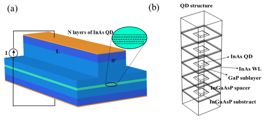
A typical InP/InAs Fabry–Perot (FP) QD laser structure was considered in this work, as shown in Figure 1a. The active QD material consists of five stacked flat-truncated-pyramidal InAs QD layers embedded in InP-lattice-matched InGaAsP ( λ Q = 1.15   μ m ) on InP (100) substrate, which is shown in Figure 1b. We considered QDs similar to those in experimental works [41,42], and the QD stacks were built as in our previous works [43,44,45,46]. In addition, the QD laser structure had a cavity length (L) of 1.5 mm and ridge width (W) of 2.3 µm as well as five active quantum dot layers. One of the facets was set as high reflectively coating of 99%, and the other was 33%.
Two types of five-layers QD stacks were considered in this work. In the uniform stack, the QDs within the same vertical column were assumed to have the same size, so that the confined energy levels of adjacent layers were well aligned and strong coherent coupling can occur. In the chirped stack, the QD size was intentionally varied from layer to layer along the growth direction, which introduces detuning of the confined states and suppresses strong vertical resonance. In the present work, chirping was introduced through variation in the QD base diameter (from 30 to 40 nm) within the stacked column, and the QD height was changed from 1.5 to 2.5 nm, which was controlled by the double-capping procedure [41,43].
Calculation of the electronic states of QDs structure was performed by using the strain-dependent 8-band k · p model that is shown in detail in Ref. [43]. To obtain the carrier lifetime of ground states (GSs) in QD structure, the transition rate of carrier of GSs was calculated first. In this work, the optical-field polarization dependence was neglected. Therefore, the transition rate can be calculated by the simplified formulae is expressed as [47]:
γ t r a n = 1 τ r = π e 2 2 m 0 2 M i j 2 I i , j 2
where m 0 denotes the free-electron mass, and I i , j represents the overlap integral between the envelope functions of an electron and a hole, which can be obtained from the calculation results of 8-band k · p model. And M i j 2 is the momentum matrix element expressed as [48],
M i j 2 = m 0 2 12 m e * E g ( E + ) E g + 2 / 3
where E g is the band gap, m e * is the electron effective mass, and is the spin-orbit interaction energy of QD material. All above parameters needed can be found in Ref. [43].
In vertically stacked QDs, coherent coupling does not only introduce an additional carrier transfer pathway but also modifies the confined-state energies through wavefunction delocalization and reduced confinement. When adjacent QDs are sufficiently aligned in energy, their confined states hybridize and form coupled states with miniband-like character. Therefore, the resonant tunneling considered in this work was associated with both carrier redistribution and a renormalization of the original localized QD energy levels induced by interdot coupling.
The physic mechanisms governing tunneling process in QDs remain a subject of ongoing debate; therefore, the detailed tunneling process will not be discussed in this paper. Instead, we directed our attention towards investigation of the impact of the carrier tunneling process on carrier transfer motions, since carrier resonant tunneling among GSs of QDs certainly occurs, thus leading to alteration of carrier lifetime of GSs. To study resonant tunneling, we made the following assumptions. (1) All carrier transfer channels originating from energy levels above GS of QDs are not considered. This is because these transfer channels only affect the carrier transition rates between wetting layer (WL) and excited state (ES), or between ES and GS. And (2) non-resonant tunneling among GSs of QDs is not considered, such as phonon-assisted carrier tunneling from the GSs of one QD to another GSs of another QD. This is because this non-resonant tunneling may occur under specific conditions, such as in strongly coupled QDs at high temperature. (3) Field-induced detuning due to doping, applied bias, or internal electric fields are not included. Based on the above assumptions, the increased carrier lifetime of GS is totally attributed to the resonant tunneling effect only.
After the GS lifetimes were calculated for the chirped and uniform stacked structures, the lifetime difference was used to estimate an effective tunneling time. Physically, this tunneling time is mainly governed by the degree of energetic alignment and wavefunction overlap between adjacent QDs. Therefore, the most influential structural factors are the inter-layer spacer thickness, the QD size dispersion along the vertical stack, and the resulting confinement-energy detuning.
To simulate the lasing behaviors of a FP QD laser, four-level coupled rate equations with a pair of forward and backward travelling wave equations were used, i.e., the excited state energy (ES), the ground state (GS), the lowest edge energy of the continuum band of wetting layer (WL), and the lowest edge energy of the InGaAsP separate-confinement heterostructure (SCH). In addition, it was assumed that only cascaded relaxations between the states are taken into consideration (i.e., the possible complex tunneling process among high energy states are not considered).
To account for the inhomogeneous broadening of density of states caused by QD sizes dispersion in-plane in fabrication growth process, the whole QD ensemble was divided in N groups (N = 15 in this work). The QDs belonging to the same group were assumed to be identical, which means the QDs have the same interband transition energies ω ¯ i , m and occupation probabilities in the confined states ρ i , m , where the index i (=1, …, N) indicates ith QD group, and the index m = GS and ES is referred to the GS and ES state, respectively. The equations used in our model are expressed as follows.
The forward (+) and backward () time-domain travelling wave equation are expressed by
η c E ± t ± E ± z = α i 2 E ± z , t + S ± z , t j P ± z , t
where the intrinsic waveguide loss is α i ; and E ± , S ± , and P ± are electric field amplitude, spontaneous emission noise source, and the optical susceptibility of the QD active medium, respectively. The detailed expressions can be found in Ref. [11]. The background effective refractive index of the guide mode is η ; and c is the light velocity in vacuum.
For a Fabry–Perot cavity, the boundary conditions can be written as
E + 0 , t = r 0 E 0 , t
E L , t = r L E + L , t
where L is the cavity waveguide length, and r 0 , and r L are the left and right facet reflectivity of electric field, respectively.
The four-level rate equations for SCH, WL, ES and GS, including the resonant tunneling, are expressed by [11]:
d N S C H d t = η i J e Δ z W N S C H τ r S C H N S C H τ c W L + N W L τ e W L
d N W L d t = N S C H τ c W L N W L τ r W L N W L τ e W L i = 1 N G i τ c E S N W L 1 ρ i , E S + i = 1 N N i , E S τ e E S
d N i , E S d t = G i τ c E S N W L 1 ρ i , E S + N i , G S τ e G S 1 ρ i , E S N i , E S τ e E S N i , E S τ s E S N i , E S ρ i , E S τ A u E S N i , E S τ c G S 1 ρ i , G S j Δ z ω ¯ i , E S E + p i , E S + * E + * p i , E S + + ( E p i , E S * E * p i , E S )
d N i , G S d t = N i , E S τ c G S 1 ρ i , G S N i , G S τ e G S 1 ρ i , E S N i , G S τ s G S N i , G S ρ i , G S τ A u G S + N i , G S ρ i , G S τ t u n G S j Δ z ω ¯ i , G S E + p i , G S + * E + * p i , G S + + ( E p i , G S * E * p i , G S )
where J is the applied current density, along with QD ridge width W to represent the input excitation; η i is the internal quantum efficiency; N W L and N S C H are the total number of carriers in WL and SCH, respectively; the total number of carriers in GS and ES are N i , G S   a n d   N i , E S in ith QD group, respectively; the corresponding occupation probabilities of GS and ES in ith QD group are ρ i , G S and ρ i , E S , respectively; the microscopic polarizations of GS and ES in ith QD group are p i , G S ± and p i , E S ± , respectively, which contribute to the total polarization P ± (the detailed expressions can be found in Ref. [11]); and the last term of (8) and (9) describes the radiative recombination in the ith QD group.
The characteristic capture times τ c W L , τ c E S , and τ c G S describe the carrier relaxation time from SCH to WL, from WL to ES within a QD, and from ES to GS within a QD, respectively. The interband recombination times in WL and SCH are τ r W L , and τ r S C H , respectively. The spontaneous emission recombination times in ES and GS are   τ s E S and τ s G S , respectively. The Auger recombination times in ES and GS are τ A u E S and τ A u G S , respectively. The interband transition energies in ES and GS in the ith QD group are ω ¯ i , E S and ω ¯ i , G S , respectively. Note the resonant tunneling effect is included in (7), and τ t u n G S represents the tunneling time of GS. This tunneling time for our considered QD stacks is estimated in the following section. After making this estimation, we can subsequently compare it with experimental results to obtain a reasonable tunneling time, which will be applied to the above rate equations. Note that the tunneling time may take on a negative value if the resonant tunneling leads to a longer carrier lifetime of GS. Conversely, if the resonant tunneling has the opposite effect, the tunneling time will be a positive value. The escape times τ e W L , τ e E S   , and τ e G S are calculated from the capture time, and the functions are provided in detail in Ref. [11].
In this work, the threshold current was extracted from the simulated light-current characteristics at each operating temperature. The relative intensity noise (RIN) was calculated from the time-domain laser simulation including the spontaneous-emission noise source in the traveling-wave equations. The RIN comparison was performed under the same normalized operating condition, namely at a bias current corresponding to twice the threshold current for each laser at each temperature.

3. Results and Discussion

3.1. Electronic Coupling

The electronic coupling within the five-layer QD stacks was investigated. In this paper, we only focused on the electronic coupling of radiative energy states, i.e., the GSs. Our QD structure was constructed based on the QDs detailed in Ref. [43], with a QD surface density of 4 × 10 10   c m 2 . The QD height and diameter fell within the ranges of 1.5–2.5 nm and 30–40 nm, respectively. This yielded an average distance between adjacent in-plane QDs, which was larger than the QD base diameter. Consequently, the lateral incoherent coupling in our structure could be neglected unless the in-plane distribution of QDs was significantly uneven. As for lateral coherent coupling, it may exist to some extent, considering that a substantial fraction of in-plane QDs shares similar sizes. However, it is difficult to investigate with our QD stacks structure due to the strong dependency of the in-plane QDs distribution on the growth process, leading to varying QD size dispersion even within a single QD layer.
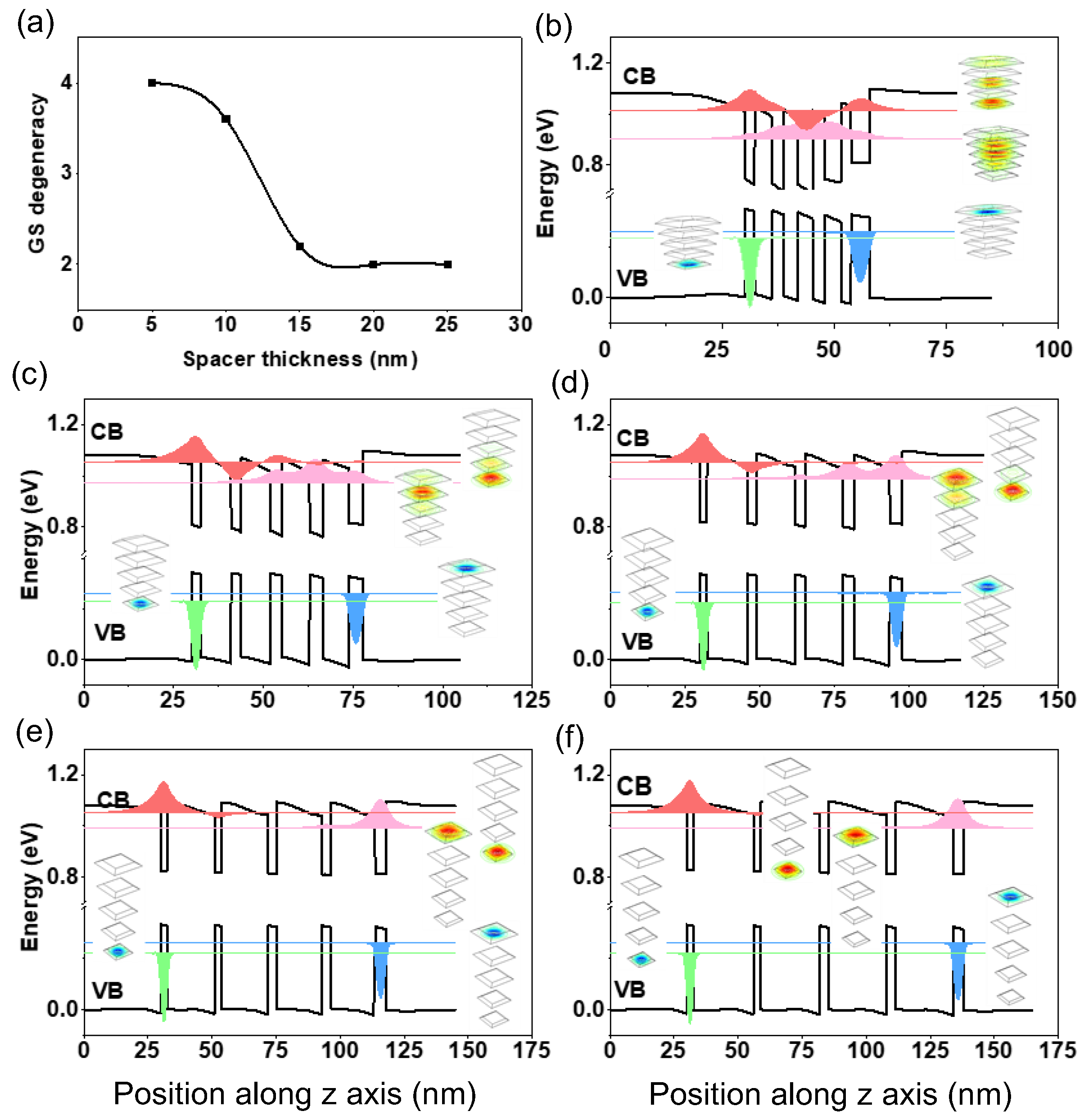
More importantly, vertical coupling in our study is highly influenced by two critical factors: the thickness of the inter-layer spacer and the dispersion of QD sizes within the same column. The growth process of QDs allows us to effectively control both of them. To investigate these effects, two types of five-layer stacks were considered as follows: chirped stacks, in which the QD base diameter varies from layer to layer, and uniform stacks, in which the QDs in the same column have the same size. The chirped stack was first used to examine the role of the inter-layer spacer thickness. In this case, the InGaAsP spacer layer controls the degree of vertical wavefunction overlap and therefore the strength of strain-induced coherent coupling. Figure 2a shows the variation in the average GS degeneracy indicator with inter-layer spacer thickness. In this paper, this quantity should not be interpreted as a literal increase in the total number of GS-derived states. Instead, it is used as an indicator of the extent to which the GSs of adjacent QDs become energetically clustered due to coherent vertical coupling. When the spacer layer is thin, stronger interdot coupling causes the GSs of neighboring QDs to hybridize into closely spaced coupled states with miniband-like character. As the spacer thickness increases, the wavefunctions become more localized in individual QDs, the hybridization becomes weaker, and the GS clustering is gradually suppressed. When the spacer thickness exceeds about 15 nm, the degeneracy indicator approaches its minimum value. Figure 2b–f depict the band structures and wavefunctions of the lowest electron GS and the highest hole GS for chirped QD stacks with spacer thicknesses of 5, 10, 15, 20, and 25 nm, respectively. It is evident that, as the inter-layer spacer thickness increases, the electron wavefunction becomes more localized, and delocalization disappears when the inter-layer spacer exceeds 15 nm in thickness. However, the inter-layer spacer has minimal impact on the hole wavefunctions, as they exhibit little delocalization with varying spacer thickness. As a result, strain-induced electronic coupling of GSs is typically not a significant consideration in many QD devices, since the inter-layer spacer thickness in QD stacks generally exceeds 30 nm. Our calculation results align closely with the findings of previous experimental studies [32,33,34].
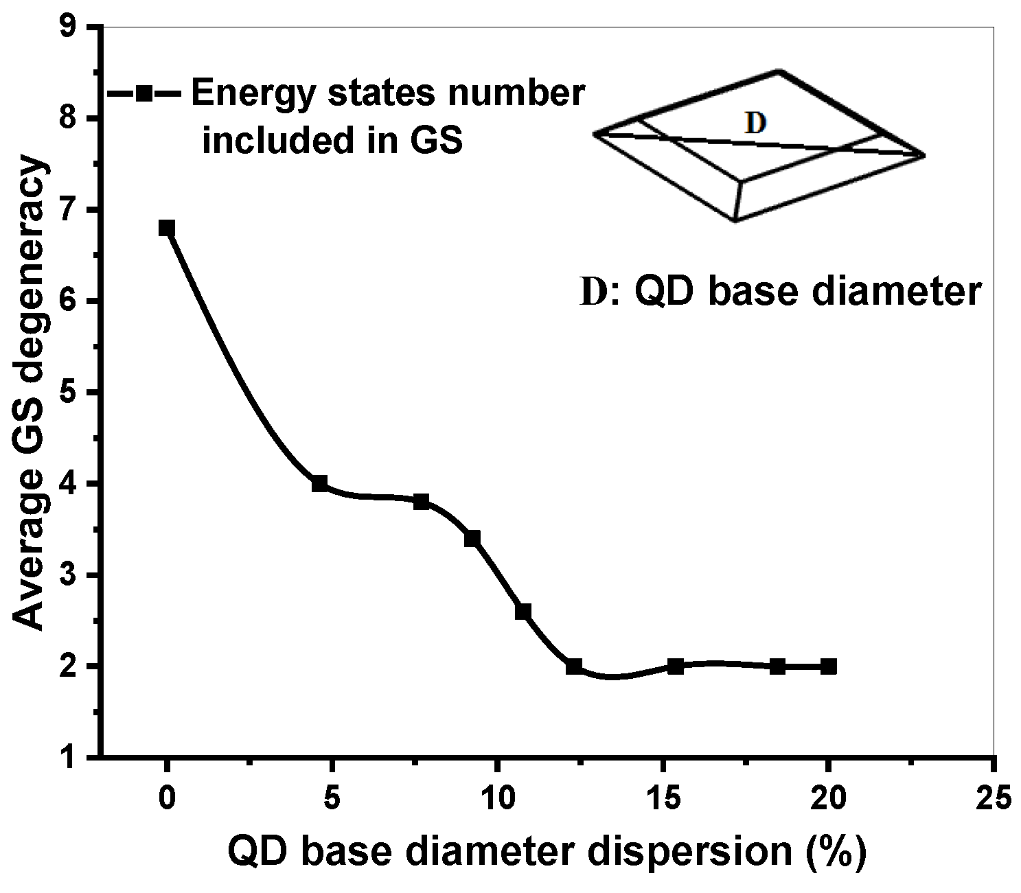
Subsequently, we maintained a constant inter-layer spacer thickness of 30 nm and focused on the impact of QD size dispersion only within the same column on vertical coupling. In our QD stacks structure, we only considered variations in QD base diameter, as the dispersion in QD height can be effectively suppressed during the QD growth process using techniques such as double capping procedure [41]. The results in Figure 3 show that the average GS degeneracy indicator decreases as the QD base diameter dispersion increases. When the diameter dispersion exceeds about 12%, the GS clustering reaches its minimum value, indicating that strong GS resonant coupling is largely suppressed. This behavior reflects the fact that size-induced detuning shifts the confined energies of different QDs away from resonance and therefore weakens the formation of coupled GS states.
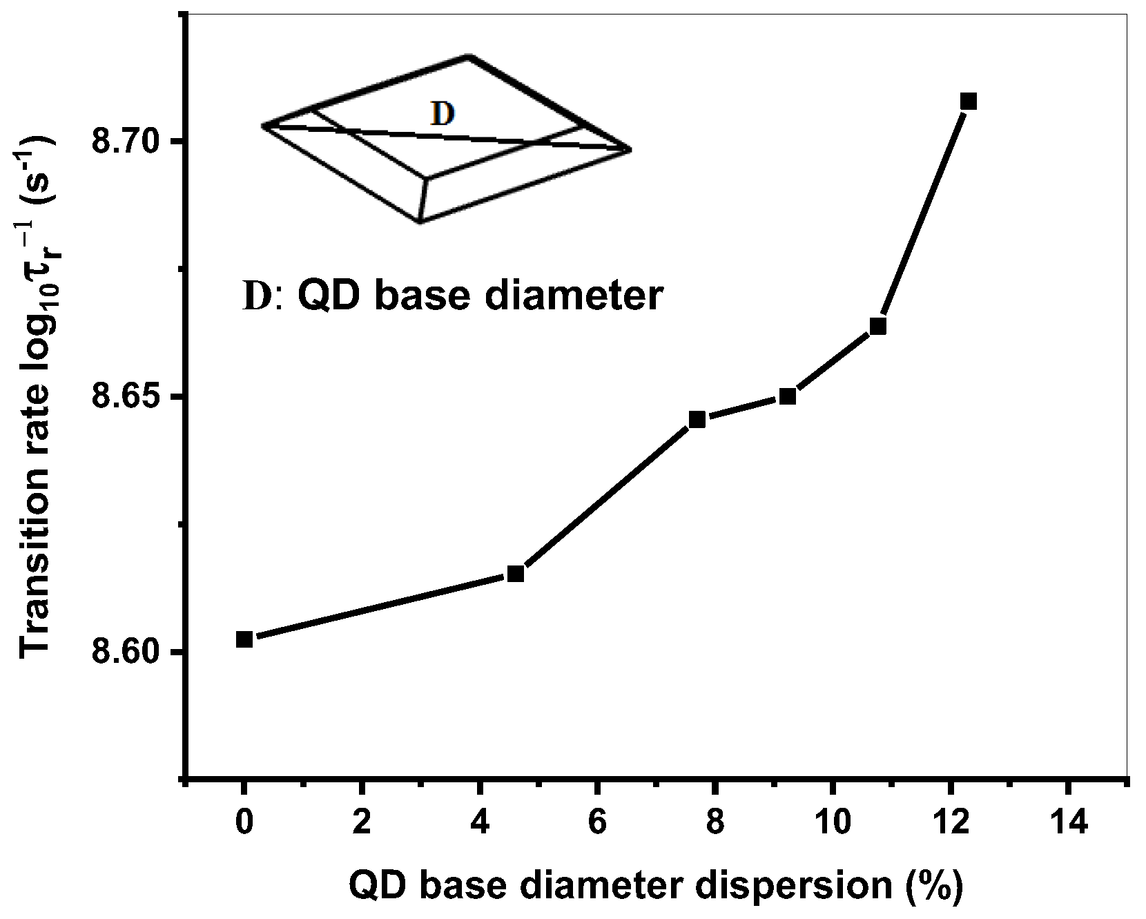
The impact of vertical resonant coupling on the GS transition is further examined in Figure 4, which shows the calculated transition rate as a function of QD base diameter dispersion. As the diameter dispersion increases, the transition rate also increases. This indicates that strong vertical coherent coupling reduces the GS transition rate and prolongs the effective GS carrier lifetime. Physically, resonant tunneling between coupled QDs introduces additional redistribution channels for carriers confined in the GS; so, the carrier population is less efficiently confined to a single localized radiative state. As a result, the radiative GS transition is weakened and the effective carrier lifetime becomes longer in the strongly coupled case.
It should be noted that the trend in Figure 4 does not exactly follow that in Figure 3, even though both are controlled by the same structural parameter. This is because the average GS degeneracy indicator and the optical transition rate characterize different aspects of the coupled QD system. The former mainly reflects the degree of GS state clustering caused by coherent coupling, whereas the latter depends directly on the detailed electron–hole overlap and the precise confinement-energy distribution. Therefore, after the GS clustering has nearly saturated, the transition rate may continue to change noticeably with the increase in QD size dispersion.
These results show that resonant tunneling cannot be ignored in the carrier-dynamics description of QD lasers and can significantly influence their optical properties.
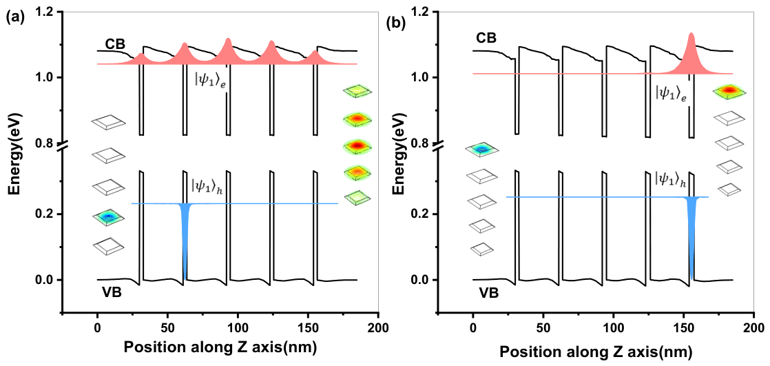
To understand the carrier resonant tunneling further, we compared a five-layer chirped QD stack, which should lack GS resonant coupling, with a uniform five-layer QD stack, which should have strong GS resonant coupling. In Figure 5, the band structures and wavefunctions for the lowest ground state of the chirped and uniform QD stacks are shown. It is evident that the miniband effect and wavefunction delocalization are only present in the uniform QD stacks. The asymmetric localization of the highest hole state in the uniform stack arises from the combined effects of the strain distribution, valence-band profile, and interdot coupling, and therefore, the hole state does not necessarily localize at the geometric center of the stack. Then, we calculated the carrier lifetimes for the chirped and uniform QD stacks, which are 1.65612 ns and 1.95929 ns, respectively. The prolonged carrier lifetime observed in the uniform QD stacks is attributed to carrier tunneling process. Therefore, a carrier tunneling time of 303 ps was obtained for the uniform QD stacks. It is true that QD coupling in-column in real fabricated QDs stacks should not be as strong as in the above uniform QD stacks (because QDs in a column are entirely aligned and uniform); thus, our calculated tunneling time may be slightly larger than that in real fabricated QDs stacks. Nevertheless, the calculated results remain reasonable, because the calculated results have the same order of magnitude as measured in prior experiments [49]. The measured resonant tunneling time stands at approximately 350 ps, including both tunneling in-column and in-plane, independent of the temperature. Considering both in-plane and in-column resonant tunneling, it is justified to apply a tunneling time of 350 ps to the above rate equations, with further details provided in the subsequent section.

3.2. Optical Properties of InAs/InP FP QD Lasers

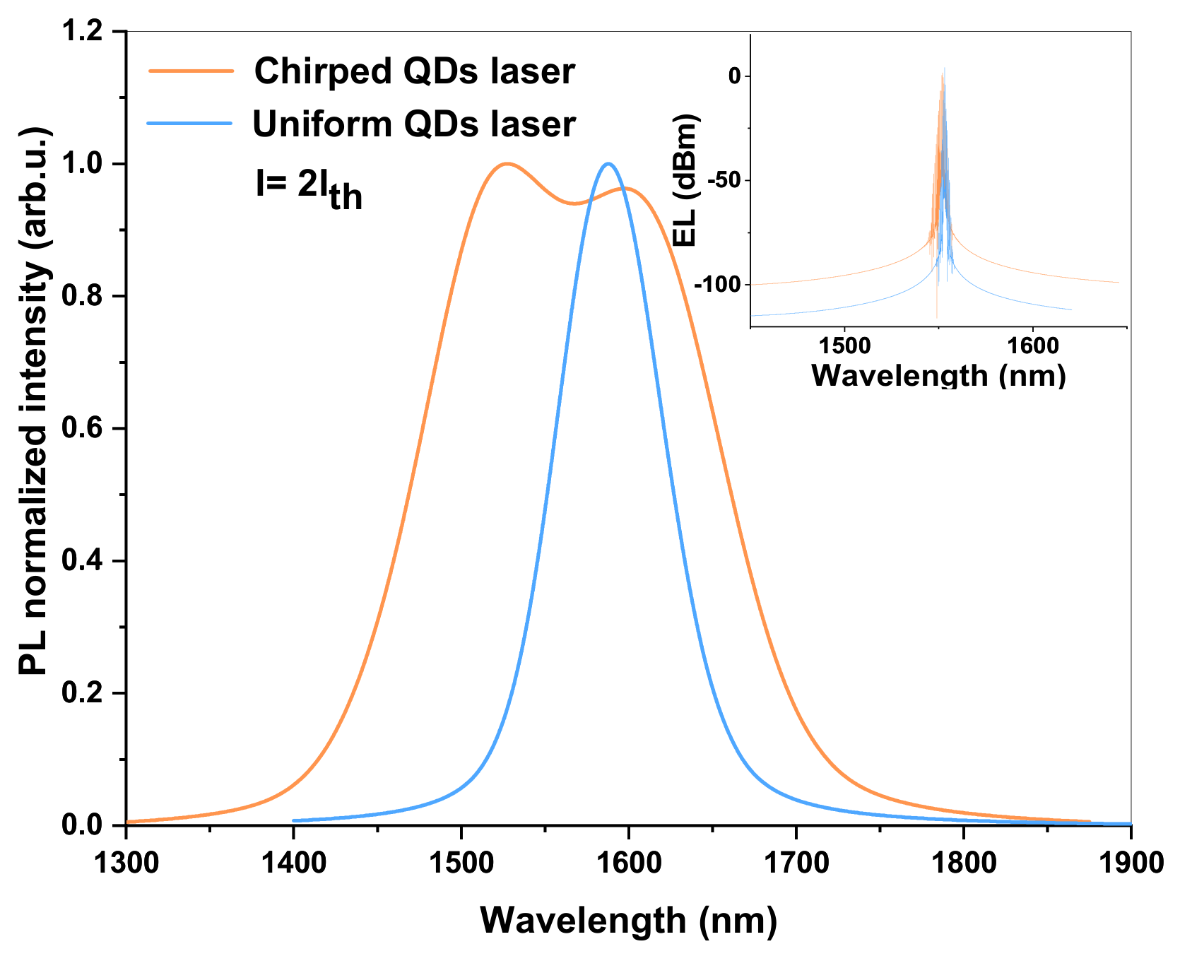
The above rate equations were used for an active region of a QD laser comprising either five-layer chirped or five-layer uniform QD stacks. The FP laser operates under continuous-wave (CW) injection current. Figure 6 displays the normalized photoluminescence (PL) spectra of the QD active region for the chirped and uniform QD stacks at room temperature (298 K). The inset shows the electroluminescence (EL) spectrum. The full width at half maximum (FWHM) of the PL spectrum is 193 nm for the chirped QD laser, and it is 96 nm for the uniform QD laser. The PL spectral broadening of the uniform QD laser is thanks to in-plane QD inhomogeneous size dispersion, while the ultrabroad PL spectral broadening of the chirped QD laser results from both in-plane and in-column QD inhomogeneous size dispersion. Even though the same in-plane QD dispersion for both the uniform and chirped QD stacks is used, the ultra-broadened PL spectrum of the chirped QD laser indicates the chirped QD stacks generating a broad gain bandwidth.
It should be noted that the PL features shown in Figure 6 correspond to the dominant ensemble emission bands rather than separately resolved peaks from every individual QD layer in the stack. In the chirped structure, multiple transitions overlap under inhomogeneous broadening; so, only the dominant spectral features remain clearly visible.
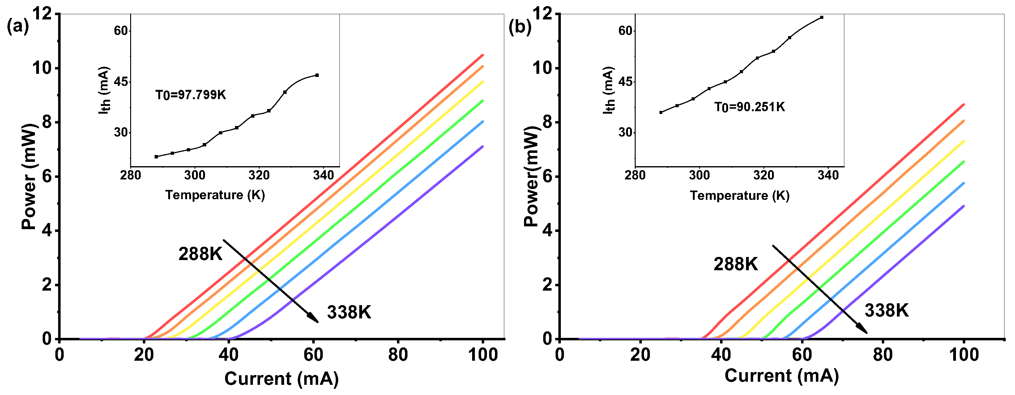
The effect of carrier tunneling on the threshold current of InAs/InP QD-based FP laser was explored first. In Figure 7, the light power-current curve depicts the output power with injection current for a temperature range from 288 K to 338 K. The insets provide the threshold current as a function of temperature. At 288 K, the threshold current is approximately 22 mA for the chirped QD laser and 35 mA for the uniform QD laser. Varying the temperature from 288 K to 338 K, the threshold current ranges from 22 mA to 45 mA for the chirped QD laser and from 35 mA to 62 mA for the uniform QD laser. Moreover, the characteristic temperature for the chirped and uniform QD laser are about 97.8 K and 90.3 K, respectively. In comparison to the chirped QD laser, the higher threshold current of the uniform QD laser is attributed to the increased carrier lifetime of GS due to carrier resonant tunneling. Similarly, the smaller characteristic temperature is also caused by carrier resonant tunneling, since it introduces more noise during carrier redistribution in QDs. It is worth to noting that previous experimental studies [50,51] on similar InAs/InP QD lasers with chirped and uniform QD stacks align with the above theoretical calculations. Based on their studies, the chirped QD laser has a broader gain bandwidth compared with the uniform QD laser, and the threshold current of the chirped QD laser is smaller than that of the uniform QD laser. So, it is reasonable to attribute the larger threshold current of the uniform QD laser to the resonant tunneling within the uniform QD stacks in their experiments.
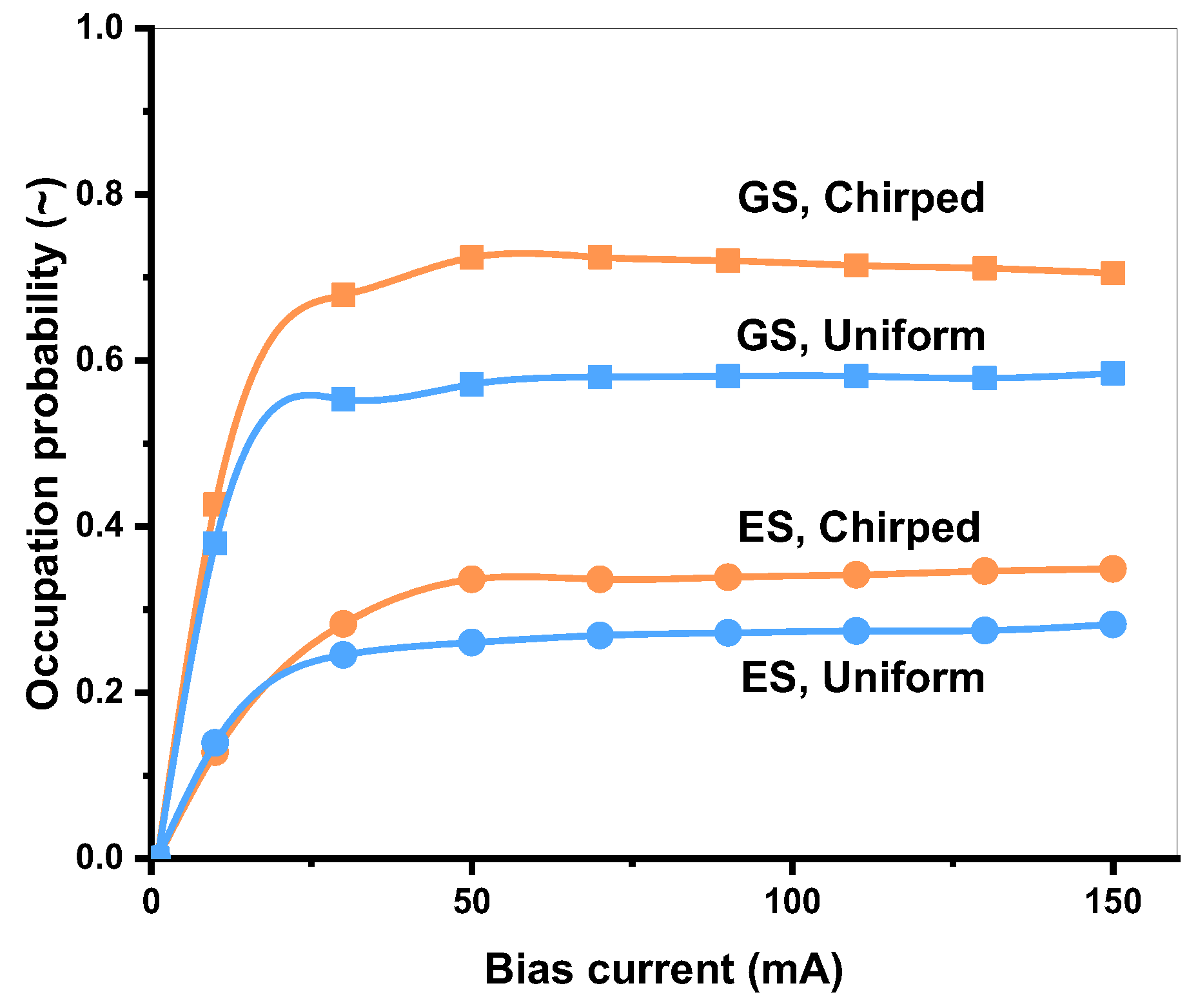
To illustrate the effect of resonant tunneling on the carriers of GS, we calculated the carrier occupation probability of ground states (GS) and excited states (ES) for both the chirped and uniform QD lasers, as shown in Figure 8. The orange lines represent the GS (square) and ES (circle) occupation probabilities of the chirped QD laser, while the blue lines show the GS (square) and ES (circle) occupation probabilities of the uniform QD laser. For electrons, GS exhibits higher filling efficiency than ES for both types of lasers, and the chirped QD laser shows a higher filling efficiency than the uniform QD laser for both GS and ES, which suggests stronger electron confinement in the chirped QD stacks. The resonant coupling of GS in the uniform QD stacks induces miniband effect, elevating several GS energy levels and resulting in relatively lower confinement. Above all, the higher carrier occupation probability enhances QD laser performance, such as reducing the threshold current and improving the thermal stability.
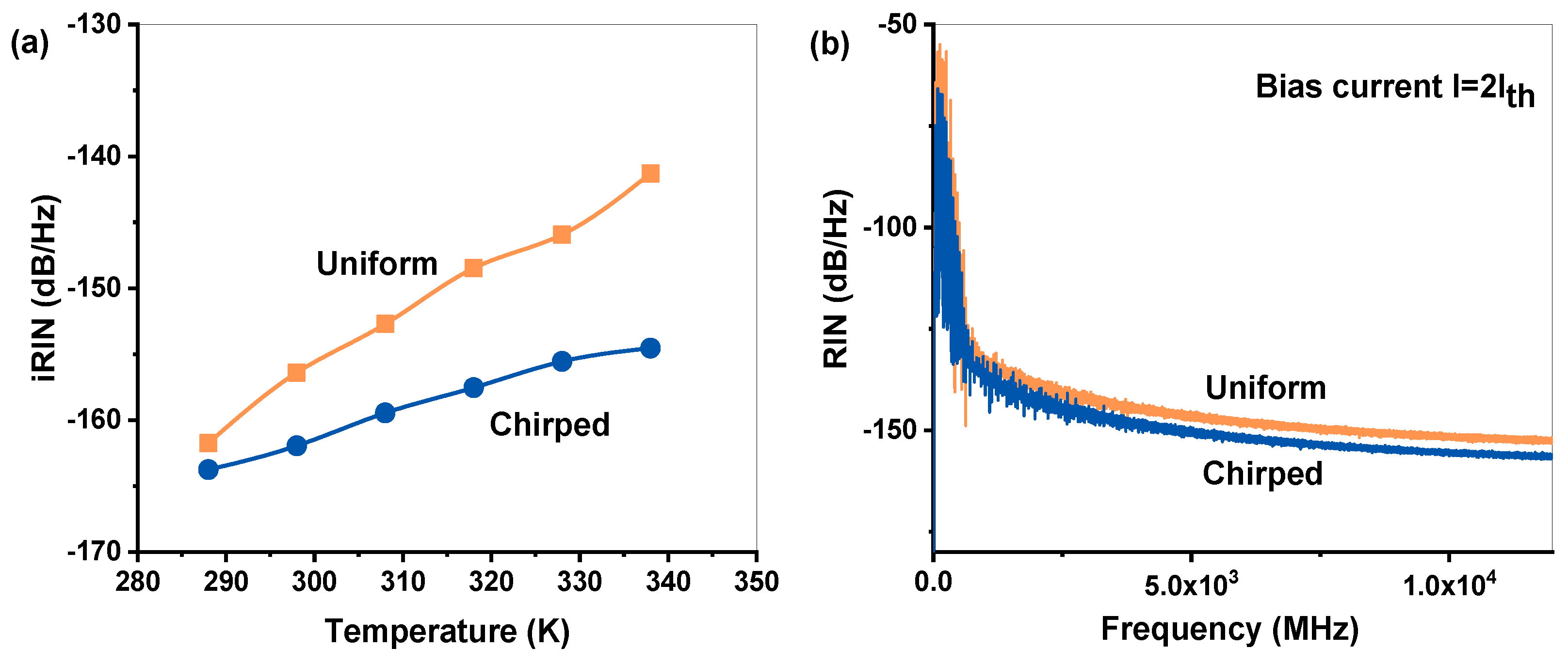
Finally, we calculated and compared the relative intensity noise (RIN) of the chirped and uniform QD laser. Figure 9a illustrates the average RIN values between 1 MHz and 10 GHz as a function of temperature for the chirped and uniform QD laser, respectively. These RIN values are measured at the same normalized bias current at each temperature (a two-times the threshold current), for the chirped QD laser with a bias current of 70 mA and the uniform QD laser of 90 mA. It is shown that the RIN of the chirped QD laser is smaller than that of the uniform QD laser at each temperature, and the difference of RIN of the two types of lasers becomes very large at a higher temperature. Furthermore, the steeper slope of blue line (chirped) compared to the orange line (uniform) indicates that the chirped QD laser exhibits superior thermal stability. Additionally, Figure 9b shows the RIN spectrum at 298 K for both the chirped and uniform QD laser, and they are calculated at a bias current equivalent to two times of each laser’s threshold current. As depicted, the RIN of the chirped QD laser remains smaller than that of the uniform QD laser. Consequently, the carrier tunneling in the uniform QD stacks indeed reduces the thermal stability of the uniform QD laser.

4. Conclusions

We conducted an investigation of electronic coupling in QD stacking structures by comparing uniform and chirped QD stacks. Our results reveal that coherent coupling between QDs must be accounted for. This is because coherent coupling enables resonant tunneling of carriers in the GS, which significantly extends the GS carrier lifetime. Consequently, GS resonant tunneling within QD stacks should be explicitly included.
Rate equation simulations of QD FP lasers, incorporating the carrier resonant tunneling effect, demonstrate that this mechanism increases the threshold current, decreases the characteristic temperature, and increases the RIN. These findings highlight the detrimental role of resonant tunneling in degrading the thermal stability of QD lasers.
Overall, this work provides comprehensive insights into the dynamics of electronic coupling in QD ensembles, offering valuable guidance for optimizing QD laser performance and advancing their potential applications.

Author Contributions

Conceptualization, F.H.; Validation, F.H.; Formal analysis, F.H.; Investigation, F.H.; Resources, F.H.; Data curation, F.H.; Writing—original draft, F.H.; Writing—review & editing, X.Z.; Supervision, X.Z.; Project administration, X.Z.; Funding acquisition, X.Z. All authors have read and agreed to the published version of the manuscript.

Funding

This research was funded by NSERC discovery grants (NSERC—Natural Sciences and Engineering Research Council).

Institutional Review Board Statement

Not applicable.

Informed Consent Statement

Not applicable.

Data Availability Statement

The original contributions presented in this study are included in the article. Further inquiries can be directed to the corresponding author.

Conflicts of Interest

The authors declare no conflict of interest.

References

  1. Akahane, K.; Yamamoto, N.; Kawanishi, T. High characteristic temperature of highly stacked quantum-dot laser for 1.55-μm band. IEEE Photonics Technol. Lett. 2010, 22, 103–105. [Google Scholar] [CrossRef]
  2. Zory, P.S., Jr. (Ed.) Quantum Well Lasers; Elsevier: Amsterdam, The Netherlands, 2012. [Google Scholar]
  3. Ohtsubo, J. Semiconductor Lasers: Stability, Instability and Chaos; Springer: Berlin/Heidelberg, Germany, 2012. [Google Scholar] [CrossRef]
  4. Bhowmick, S.; Baten, M.Z.; Frost, T.; Ooi, B.S.; Bhattacharya, P. High performance InAs/In0.53Ga0.23Al0.24As/InP quantum dot 1.55 µm tunnel injection laser. IEEE J. Quantum Electron. 2014, 50, 7–14. [Google Scholar] [CrossRef]
  5. Ustinov, V.M. Quantum Dot Lasers; Oxford University Press: Oxford, UK, 2003. [Google Scholar] [CrossRef]
  6. Ferreira, R.; Bastard, G. Capture and Relaxation in Self-Assembled Semiconductor Quantum Dots: The Dot and Its Environment; Morgan & Claypool Publishers: San Rafael, CA, USA, 2016. [Google Scholar]
  7. Narvaez, G.A.; Bester, G.; Zunger, A. Carrier relaxation mechanisms in self-assembled InGaAs/ GaAs quantum dots: Efficient P-S Auger relaxation of electrons. Phys. Rev. B 2006, 74, 075403. [Google Scholar] [CrossRef]
  8. Miska, P.; Even, J.; Dehaese, O.; Marie, X. Carrier relaxation dynamics in InAs∕InP quantum dots. Appl. Phys. Lett. 2008, 92, 191103. [Google Scholar] [CrossRef]
  9. Seebeck, J.; Nielsen, T.R.; Gartner, P.; Jahnke, F. Polarons in semiconductor quantum dots and their role in the quantum kinetics of carrier relaxation. Phys. Rev. B 2005, 71, 125327. [Google Scholar] [CrossRef][Green Version]
  10. Otto, C. Dynamics of Quantum Dot Lasers: Effects of Optical Feedback and External Optical Injection; Springer International Publishing: Cham, Switzerland, 2014. [Google Scholar]
  11. Rossetti, M.; Bardella, P.; Montrosset, I. Time-domain travelling-wave model for quantum dot passively mode-locked lasers. IEEE J. Quantum Electron. 2011, 47, 139–150. [Google Scholar] [CrossRef]
  12. Rossetti, M.; Fiore, A.; Sęk, G.; Zinoni, C.; Li, L. Modeling the temperature characteristics of InAs/GaAs quantum dot lasers. J. Appl. Phys. 2009, 106, 023105. [Google Scholar] [CrossRef]
  13. Gioannini, M.; Montrosset, I. Numerical analysis of the frequency chirp in quantum-dot semiconductor lasers. IEEE J. Quantum Electron. 2007, 43, 941–949. [Google Scholar] [CrossRef]
  14. Tong, C.Z.; Yoon, S.F.; Ngo, C.Y.; Liu, C.Y.; Loke, W.K. Rate Equations for 1.3-mm dots-under-a-well and dots-in-a-well self-assembled InAs–GaAs quantum-dot lasers. IEEE J. Quantum Electron. 2006, 42, 1175–1183. [Google Scholar] [CrossRef]
  15. Huang, H.; Deppe, D.G. Rate equation model for nonequilibrium operating conditions in a self-organized quantum-dot laser. IEEE J. Quantum Electron. 2001, 37, 691–698. [Google Scholar] [CrossRef]
  16. Lan, S.; Akahane, K.; Kawamura, K.-Y.; Okada, Y.; Kawabe, M.; Nishimura, T.; OsamuWada, O. Two-dimensional In0.4Ga0.6As/GaAs quantum dot superlattices realized by self-organized epitaxial growth. Jpn. J. Appl. Phys. 1999, 38, 2934. [Google Scholar] [CrossRef]
  17. Cornet, C.; Hayne, M.; Caroff, P.; Levallois, C.; Joulaud, L.; Homeyer, E.; Paranthoen, C.; Even, J.; Labbé, C.; Folliot, H.; et al. Increase of charge-carrier redistribution efficiency in a laterally organized superlattice of coupled quantum dots. Phys. Rev. B 2006, 74, 245315. [Google Scholar] [CrossRef]
  18. Hall, R.N.; Fenner, G.E.; Kingsley, J.D.; Soltys, T.J.; Carlson, R.O. Coherent light emission from GaAs junctions. Phys. Rev. Lett. 1962, 9, 366–368. [Google Scholar] [CrossRef]
  19. Veisi, M.; Kazemi, S.H.; Mahmoudi, M. Tunneling-induced optical limiting in quantum dot molecules. Sci. Rep. 2020, 10, 16304. [Google Scholar] [CrossRef] [PubMed]
  20. Katz, D.; Millo, O.; Kan, S.-H.; Banin, U. Control of charging in resonant tunneling through InAs nanocrystal quantum dots. Appl. Phys. Lett. 2001, 79, 117–119. [Google Scholar] [CrossRef][Green Version]
  21. Van Der Wiel, W.G.; De Franceschi, S.; Elzerman, J.M.; Fujisawa, T.; Tarucha, S.; Kouwenhoven, L.P. Electron transport through double quantum dots. Rev. Mod. Phys. 2002, 75, 1. [Google Scholar] [CrossRef]
  22. Han, D.-S.; Asryan, L.V. Output power of a double tunneling-injection quantum dot laser. Nanotechnology 2010, 21, 015201. [Google Scholar] [CrossRef]
  23. Bopp, F.; Rojas, J.; Revenga, N.; Riedl, H.; Sbresny, F.; Boos, K.; Simmet, T.; Ahmadi, A.; Gershoni, D.; Kasprzak, J.; et al. Quantum dot molecule devices with optical control of charge status and electronic control of coupling. Adv. Quantum Technol. 2022, 5, 2200049. [Google Scholar] [CrossRef]
  24. Tackeuchi, A.; Kuroda, T.; Mase, K.; Nakata, Y.; Yokoyama, N. Dynamics of carrier tunneling between vertically aligned double quantum dots. Phys. Rev. B 2000, 62, 1568–1571. [Google Scholar] [CrossRef]
  25. Abiedh, K.; Zaaboub, Z.; Hassen, F.; David, T.; Sfaxi, L.; Maaref, H. Experimental and theoretical study of thermally activated carrier transfer in InAs/GaAs multilayer quantum dots. Appl. Phys. A 2020, 126, 491. [Google Scholar] [CrossRef]
  26. Shi, B.; Xie, Y.H. Influence of coupling effect in the operation of vertically coupled quantum-dot lasers. Appl. Phys. Lett. 2003, 82, 4788–4790. [Google Scholar] [CrossRef]
  27. Bhattacharyya, J.; Zybell, S.; Winnerl, S.; Helm, M.; Hopkinson, M.; Wilson, L.R.; Schneider, H. In-plane interdot carrier transfer in InAs/GaAs quantum dots. Appl. Phys. Lett. 2012, 100, 152101. [Google Scholar] [CrossRef]
  28. Mazur, Y.I.; Tomm, J.W.; Tarasov, G.G.; Kissel, H.; Walther, C.; Zhuchenko, Z.Y.; Masselink, W.T. Interdot energy transfer in a system of coupled InAs/GaAs quantum dots. Phys. E Low-Dimens. Syst. Nanostructures 2002, 13, 255–258. [Google Scholar] [CrossRef]
  29. Liu, Y.; Wang, Y.; Liang, B.; Guo, Q.; Wang, S.; Fu, G.; Mazur, Y.I.; Ware, M.E.; Salamo, G.J. Interplay effect of excitation and temperature on carrier transfer between vertically aligned InAs/GaAs quantum dot pairs. Crystals 2016, 6, 144. [Google Scholar] [CrossRef]
  30. Tarasov, G.G.; Mazur, Y.I.; Zhuchenko, Z.Y.; Maaßdorf, A.; Nickel, D.; Tomm, J.W.; Kissel, H.; Walther, C.; Masselink, W.T. Carrier transfer in self-assembled coupled InAs/GaAs quantum dots. J. Appl. Phys. 2000, 88, 7162–7170. [Google Scholar] [CrossRef]
  31. Mazur, Y.I.; Dorogan, V.G.; Marega, E., Jr.; Tarasov, G.G.; Cesar, D.F.; Lopez-Richard, V.; Marques, G.E.; Salamo, G.J. Mechanisms of interdot coupling in (In,Ga)As/GaAs quantum dot arrays. Appl. Phys. Lett. 2009, 94, 123112. [Google Scholar] [CrossRef]
  32. Krenner, H.J.; Sabathil, M.; Clark, E.C.; Kress, A.; Schuh, D.; Bichler, M.; Abstreiter, G.; Finley, J.J. Direct observation of controlled coupling in an individual quantum dot molecule. Phys. Rev. Lett. 2005, 94, 057402. [Google Scholar] [CrossRef]
  33. Colocci, M.; Vinattieri, A.; Lippi, L.; Bogani, F.; Rosa-Clot, M.; Taddei, S.; Bosacchi, A.; Franchi, S.; Frigeri, P. Controlled tuning of the radiative lifetime in InAs self-assembled quantum dots through vertical ordering. Appl. Phys. Lett. 1999, 74, 564–566. [Google Scholar] [CrossRef]
  34. Rybchenko, S.I.; Itskevich, I.E.; Skolnick, M.S.; Cahill, J.; Tartakovskii, A.I.; Hill, G.; Hopkinson, M. Tuning of electronic coupling between self-assembled quantum dots. Appl. Phys. Lett. 2005, 87, 033104. [Google Scholar] [CrossRef]
  35. Tomm, J.W.; Elsaesser, T.; Mazur, Y.I.; Kissel, H.; Tarasov, G.G.; Zhuchenko, Z.Y.; Masselink, W.T. Transient luminescence of dense InAs/GaAs quantum dot arrays. Phys. Rev. B 2003, 67, 045326. [Google Scholar] [CrossRef]
  36. Mazur, Y.I.; Wang, Z.M.; Tarasov, G.G.; Xiao, M.; Salamo, G.J.; Tomm, J.W.; Talalaev, V.; Kissel, H. Interdot carrier transfer in asymmetric bilayer InAs/GaAs quantum dot structures. Appl. Phys. Lett. 2005, 86, 063102. [Google Scholar] [CrossRef]
  37. Zhou, X.L.; Chen, Y.H.; Zhang, H.Y.; Zhou, G.Y.; Li, T.F.; Liu, J.Q.; Ye, X.L.; Xu, B.; Wang, Z.G. Carrier tunneling effects on the temperature dependent photoluminescence of InAs/GaAs quantum dot: Simulation and experiment. J. Appl. Phys. 2011, 109, 083501. [Google Scholar] [CrossRef]
  38. Rudno-Rudziński, W.; Syperek, M.; Andrzejewski, J.; Rogowicz, E.; Eisenstein, G.; Bauer, S.; Sichkovskyi, V.I.; Reithmaier, J.P.; Sęk, G. Carrier transfer efficiency and its influence on emission properties of telecom wavelength InP-based quantum dot–quantum well structures. Sci. Rep. 2018, 8, 12317. [Google Scholar] [CrossRef]
  39. Lee, C.-S.; Guo, W.; Basu, D.; Bhattacharya, P. High performance tunnel injection quantum dot comb laser. Appl. Phys. Lett. 2010, 96, 101107. [Google Scholar] [CrossRef]
  40. Khanonkin, I.; Bauer, S.; Mikhelashvili, V.; Eyal, O.; Lorke, M.; Jahnke, F.; Reithmaier, J.P.; Eisenstein, G. On the principle operation of tunneling injection quantum dot lasers. Prog. Quantum Electron. 2022, 81, 100362. [Google Scholar] [CrossRef]
  41. Poole, P.J.; Kaminska, K.; Barrios, P.; Lu, Z.; Liu, J. Growth of InAs/InP-based quantum dots for 1.55 μm laser applications. J. Cryst. Growth 2009, 311, 1482–1486. [Google Scholar] [CrossRef]
  42. Lu, Z.G.; Poole, P.J.; Liu, J.R.; Barrios, P.J.; Jiao, Z.J.; Pakulski, G.; Poitras, D.; Goodchild, D.; Rioux, B.; SpringThorpe, A.J. High-performance 1.52 µm InAs/InP quantum dot distributed feedback laser. Electron. Lett. 2011, 47, 818–819. [Google Scholar] [CrossRef]
  43. Xiong, Y.; Zhang, X. An accurate method of modeling self-assembled InAs/InGaAsP/InP (001) quantum dot with double-capping procedure. IEEE J. Quantum Electron. 2017, 53, 2000611. [Google Scholar] [CrossRef]
  44. Huang, F.; Zhang, X. Impact of excited states transitions on polarization property of InAs/InP quantum dots. IEEE J. Quantum Electron. 2022, 58, 7100109. [Google Scholar] [CrossRef]
  45. Huang, F.; Xiong, Y.; Zhang, X. Self-assembled InAs/InGaAsP/InP quantum dots: Intraband relaxation impacted by ultrathin GaP sublayer. J. Appl. Phys. 2020, 127, 125702. [Google Scholar] [CrossRef]
  46. Xiong, Y.; Zhang, X. InAs/InP quantum dots stacking: Impact of spacer layer on optical properties. J. Appl. Phys. 2019, 125, 093103. [Google Scholar] [CrossRef]
  47. Blood, P. Quantum Confined Laser Devices: Optical Gain and Recombination in Semiconductors; OUP: Oxford, UK, 2015. [Google Scholar]
  48. Sugawara, M.; Mukai, K.; Nakata, Y.; Ishikawa, H.; Sakamoto, A. Effect of homogeneous broadening of optical gain on lasing spectra in self-assembled InxGa1−xAs/GaAs quantum dot lasers. Phys. Rev. B 2000, 61, 7595–7603. [Google Scholar] [CrossRef]
  49. Talalaev, V.G.; Tomm, J.W.; Sokolov, A.S.; Shtrom, I.V.; Novikov, B.V.; Winzer, A.T.; Goldhahn, R.; Gobsch, G.; Zakharov, N.D.; Werner, P.; et al. Tuning of the interdot resonance in stacked InAs quantum dot arrays by an external electric field. J. Appl. Phys. 2006, 100, 083704. [Google Scholar] [CrossRef]
  50. Gao, F.; Luo, S.; Ji, H.-M.; Liu, S.-T.; Lu, D.; Ji, C.; Yang, T. Single-section mode-locked 1.55-μm InAs/InP quantum dot lasers grown by MOVPE. Opt. Commun. 2016, 370, 18–21. [Google Scholar] [CrossRef]
  51. Gao, F.; Luo, S.; Ji, H.-M.; Liu, S.-T.; Xu, F.; Lv, Z.-R.; Lu, D.; Ji, C.; Yang, T. Ultrashort pulse and high power mode-locked laser with chirped InAs/InP quantum dot active layers. IEEE Photonics Technol. Lett. 2016, 28, 1481–1484. [Google Scholar] [CrossRef]
Figure 1. (a) Schematic of a QD Fabry–Perot laser with a cavity length L and ridge width W; and (b) geometry of five-layer truncated pyramid InAs QD stacks.
Applsci 16 04161 g001
Figure 2. (a) Average GS degeneracy indicator of each QD in the stacked column as a function of inter-layer spacer thickness for the chirped QD stacks. (bf) Band structures and wavefunctions of the lowest electron GS (red), highest hole GS (blue), and the corresponding coupled states for chirped QD stacks with inter-layer spacer thicknesses of 5, 10, 15, 20, and 25 nm, respectively. CB and VB denote the conduction-band and valence-band edges, respectively. Insets show the corresponding three-dimensional probability density distributions for electrons and holes.
Applsci 16 04161 g002
Figure 3. Average GS degeneracy of each QD in the column stacks as a function of QD base diameter dispersion.
Applsci 16 04161 g003
Figure 4. Carrier transition rate as a function of QD base diameter dispersion. The inset shows the definition of QD base diameter.
Applsci 16 04161 g004
Figure 5. Band structures and wavefunctions of the lowest electron state and the highest hole state for (a) uniform QD stacks and (b) chirped QD stacks. CB and VB denote the conduction-band and valence-band edges, respectively. Insets show the corresponding three-dimensional probability density distributions for electrons and holes.
Applsci 16 04161 g005
Figure 6. PL emission spectrum of chirped and uniform QD lasers at 298 K under CW injection current (I = 2Ith). The inset shows the corresponding EL emission spectrum.
Applsci 16 04161 g006
Figure 7. Temperature dependence of light-current characteristics for the (a) FP laser with chirped QD stacks and (b) FP laser with uniform QD stacks. The insets show the threshold current of the two lasers as a function of temperature, and the temperature varies from 288 K to 338 K.
Applsci 16 04161 g007
Figure 8. Carrier occupation probability of GS and ES as a function of injected current at 298 K. The orange lines represent the GS (square) and ES (circle) occupation probabilities of chirped QD laser, while the blue lines show the GS (square) and ES (circle) occupation probabilities of uniform QD laser.
Applsci 16 04161 g008
Figure 9. (a) Comparison of average RIN between 1 MHz to 10 GHz as a function of the temperature ranging from 288 K to 338 K for both chirped and uniform QD lasers, respectively; and (b) RIN spectrum for chirped and uniform QD lasers with bias current I = 2Ith at a temperature of 298K.
Applsci 16 04161 g009
Disclaimer/Publisher’s Note: The statements, opinions and data contained in all publications are solely those of the individual author(s) and contributor(s) and not of MDPI and/or the editor(s). MDPI and/or the editor(s) disclaim responsibility for any injury to people or property resulting from any ideas, methods, instructions or products referred to in the content.