1. Introduction
The explosive growth of mobile data traffic, driven by the deployment of 5G and beyond networks, has placed unprecedented demands on wireless communication systems. To meet the stringent requirements for high data rates and spectral efficiency, modern wireless communication systems increasingly employ complex multicarrier modulation schemes such as Orthogonal Frequency-Division Multiplexing (OFDM) [
1,
2,
3,
4]. A key characteristic of these signals is their high peak-to-average power ratio (PAPR), which forces power amplifiers (PAs) to operate frequently in power back-off regions to maintain linearity. Consequently, PAs, as the most power-consuming components in radio-frequency (RF) transmitters, must achieve high efficiency not only at peak power but also across a wide dynamic range. This challenge becomes particularly pronounced in broadband communication scenarios, such as multi-band base stations and software-defined radios, where the power amplifier is required to maintain high efficiency and linearity over a wide operating frequency range [
5,
6,
7].
Among various efficiency-enhancement architectures, the Doherty power amplifier (DPA), invented by W. H. Doherty in 1936, has been widely adopted due to its simple concept of active load modulation [
8,
9]. The conventional Doherty power amplifier (DPA) architecture employs a quarter-wavelength (λ/4) impedance inverter to modulate the load impedance seen by the carrier amplifier, thereby enhancing efficiency under 6 dB output power back-off conditions [
3,
10,
11,
12]. However, the conventional quarter-wavelength impedance inverter used in Doherty power amplifiers inherently exhibits narrowband behavior, which fundamentally limits load modulation and restricts the achievable operating bandwidth in broadband DPA designs. Recent studies have explored alternative load modulation networks and transformer-based solutions to mitigate this limitation and achieve extended bandwidth performance across wider frequency ranges [
12,
13,
14].
Extensive research has been conducted to break this bandwidth limitation. Early efforts focused on structural modifications. For example, K. Bathich et al. [
15] adjusted the load modulation trajectory and reduced the impedance transformation ratio, reaching 41–55% drain efficiency at 6 dB back-off over 1.7–2.6 GHz. R. Darraji et al. [
16] employed digital techniques to alleviate the constraints of the impedance transformer, successfully expanding the bandwidth from 180 MHz to 500 MHz. M. N. A. Abadi et al. [
17] utilized a low-order impedance matching network to replace conventional transmission lines, achieving 47–57% back-off efficiency within the 700–950 MHz range, while further incorporating an LC resonant network into the optimized output combiner to yield a 30% increase in fractional bandwidth. While these methods have advanced the state of the art, they often involve trade-offs between bandwidth, efficiency, circuit complexity, and harmonic control.
Recent developments in continuous-mode theory—including generalized continuous Class-F implementations and continuous-mode formulations—provide a comprehensive theoretical framework in which the fundamental and harmonic impedance trajectories at the transistor’s current source plane can be continuously adjusted over frequency and power levels, enabling broader bandwidth and high efficiency in broadband PA designs [
18,
19]. By introducing continuous tuning parameters (e.g., α, β, γ in Equation (1)), a continuum of optimal impedances is defined rather than a single point. This expanded impedance solution space relaxes the matching network’s constraints, making wideband impedance transformation more feasible. When applied to DPA design, the continuous mode allows the carrier amplifier’s fundamental and harmonic impedances to vary appropriately over frequency and power levels, thereby broadening bandwidth [
20,
21].
Notwithstanding these advances, a critical challenge persists: the co-design of broadband impedance matching and effective harmonic suppression. Traditional designs often treat the output matching network and the harmonic control network as separate, cascaded stages. This “separate-and-cascade” approach not only increases circuit size and introduces additional parasitic losses, but also creates impedance discontinuities that can degrade overall efficiency and bandwidth. Harmonic suppression has been demonstrated as a key technique for complying with stringent spectral mask requirements and improving power amplifier efficiency. In particular, high-order harmonic suppression networks can reduce out-of-band emissions while optimizing waveform shapes for improved PAE, as shown in recent Doherty PA designs [
22,
23,
24].
To address this co-design challenge holistically, this paper proposes a novel design methodology that integrates a high-order filter prototype directly into the PA’s output matching network. The core innovation lies in leveraging the amplitude-frequency response of the filter itself to perform dual functions: (1) enabling broadband impedance transformation from the optimal device impedance to the 50 Ω load, and (2) providing intrinsic suppression of the 2nd and 3rd harmonics by creating attenuation poles at those frequencies. This integrated approach eliminates the need for a separate harmonic trap, reducing circuit complexity and loss. We apply this methodology to design a 1.6–2.2 GHz high-efficiency continuous-mode Doherty-like PA based on a GaN HEMT (CGH40010F).
2. Principles of Circuit Design
2.1. Design Space for Expanding Continuous-Mode Theory
The concept of continuous-mode power amplifiers derives from the generalization of classical high-efficiency amplifier classes. This theoretical framework represents a paradigm shift in high-efficiency PA design, moving from the pursuit of discrete frequency-specific optimum impedances toward the utilization of a continuous impedance space to maintain high efficiency over a bandwidth. By unifying continuous B/J-mode, continuous F-mode, and other related models through the continuous-mode expansion approach, three tunable parameters—α, β, and γ—are incorporated into the drain voltage formulation of the amplifier. In the proposed design, the tuning parameters (α, β, γ) define a continuum of impedance solutions, rather than a single discrete optimum. This extends the high-efficiency operating region into a continuous zone on the Smith chart. Consequently, moderate variations in α, β, or γ do not cause abrupt degradations in efficiency or output power. Instead, such variations result in a smooth impedance shift within the permissible high-efficiency region, thereby preserving near-optimal waveform shaping at the device intrinsic plane. Thus, the generalized drain voltage waveform for such continuous modes can be expressed as a function of the conduction angle (θ) together with a set of adjustable parameters (α, β, γ), yielding the following comprehensive expression:
When α = 1, β = 0, and γ = 0, the above Formula (1) represents the continuous B/J type voltage waveform; when α = 1.5, β = 0.5, and γ = 0, the characteristic waveform of the continuous F-class mode is obtained. Different values of α and β can define different continuous types. Combined voltage and current waveforms can provide the optimal impedance solution for a continuous model. To ensure the physical realizability of the generalized waveform, the parameters
,
, and
in Equation (1) must satisfy the non-negative voltage constraint Equation (2):
This condition is essential to avoid unphysical operating states and potential device breakdown. Specifically, in the continuous Class-F mode (
,
), the tuning parameter
is constrained within the interval
, ensuring that the term
remains non-negative. This restriction preserves the drain voltage swing within the safe operating region of the CGH40010F GaN HEMT. This preventing unphysical voltage excursions and ensuring that the device operates reliably within its safe operating area (SOA).
In Equation (3), the parameters and define the fundamental current–voltage boundaries of the transistor. Here, denotes the knee voltage that separates the linear and saturation operating regions, while corresponds to the maximum peak drain current. For the CGH40010F GaN HEMT used in this work, these parameters were extracted from the device’s pulsed I–V characteristics, which effectively decouple self-heating and trapping effects. represents the conventional optimal load resistance for Class-B operation. Equations (4) and (5) describe the fundamental () and second () harmonic impedances, respectively, which can be derived from the Fourier analysis of the current waveform by varying the parameters α, β, and γ. As α, β, and γ vary continuously, these impedances trace out contours in the complex plane rather than converging to fixed points. This encapsulates the essence of continuous-mode design: the design objective evolves from matching a single impedance point to matching an entire impedance region. Such flexibility is crucial for broadband matching, as it relaxes the constraints on the matching network from a precise point to a broader area, significantly easing the difficulty of wideband impedance transformation. For Doherty power amplifiers (DPAs), this theory enables the fundamental and harmonic impedances of the carrier amplifier to vary appropriately across both frequency and power-back-off levels, which is key to extending its operational bandwidth.
The Peaking Amplifier of the DPA is designed in a continuous mode, ensuring its output impedance remains within the hybrid continuous impedance space. As input power increases, the Peaking Amplifier performs active modulation, enabling the Carrier Amplifier’s fundamental output impedance to transition from low-power to high-power regions while meeting corresponding second-harmonic impedance matching requirements. This is the core idea of continuous mode: transforming a single optimal impedance point into a cluster of optimal complex impedance points, thereby expanding the amplifier’s impedance solution space, making impedance matching easier to achieve, and thus broadening the bandwidth.
2.2. New Integrated Matching Method Based on High-Order Filtering Prototype
To address the intrinsic bandwidth limitations of conventional matching networks, this work employs a co-design approach founded on a low-pass filter prototype. While the design of the input matching network is relatively straightforward—chiefly aimed at achieving conjugate matching for the fundamental signal—the output matching network (OMN) plays a more critical and multifunctional role. The OMN must concurrently achieve broadband impedance transformation from the transistor’s optimum impedance to a 50 Ω load, maintain low insertion loss across the operating band, and deliver high rejection at the second and third harmonics. Consequently, the output network must inherently possess a filter-like amplitude-frequency response.
Therefore, The design process begins by determining the required order
of the low-pass filter and its corresponding normalized prototype parameters
based on predefined specifications for passband ripple, cutoff frequency, and stopband attenuation. Subsequently, the actual values of the lumped elements (inductors
and capacitors
) for the low-pass filter, which incorporates impedance transformation, are calculated using the following transformation Equation (6):
In these expressions, denotes the cutoff frequency of the filter. In this design, the cutoff frequency used for the initial analytical synthesis of lumped elements is set to 2.4 GHz. This value is selected to maintain a sufficient guard band with respect to the fundamental operating band (1.6–2.2 GHz), thereby ensuring low insertion loss across the passband. represents the source impedance seen from the transistor plane into the matching network. For the CGH40010F device employed in this work, is taken as the real part of the optimum load impedance (), which is extracted from load-pull simulations. is chosen as 17.5 Ω for the initial calculation of the lumped inductance and capacitance values. The formulas provide a theoretical bridge between the filter parameters and the practical circuit implementation.
Once the lumped element values are determined, they are transformed into distributed microstrip structures for circuit fabrication. In this low-pass filtering topology, a shunt capacitor (
) is typically realized using a low-impedance (
) microstrip line or an open-circuited stub, while a series inductor (
) is implemented using a high-impedance (
) microstrip line. Initial values for
and
were chosen based on the filter prototype synthesis while respecting fabrication limits. Specifically,
was set to 100 Ω to realize series inductors effectively within a compact layout, and
was set to 20 Ω to provide adequate shunt capacitance while keeping the microstrip width practically feasible. The electrical length
of each microstrip section is given by the following design Equation (7):
The corresponding physical length
of the microstrip line is then obtained from the electrical length
and the guided wavelength
by the following Formula (8).
For clarity, the physical lengths corresponding to the inductor and capacitor sections can be explicitly expressed as Formula (9):
where
and
denote the guided wavelengths on the high-impedance and low-impedance lines, respectively.
These physically derived dimensions serve as initial values for subsequent joint optimization in electromagnetic (EM) simulation software. This co-optimization process ensures that the matching network meets its performance targets—including broadband impedance transformation and harmonic suppression—while remaining aligned with the theoretical design objectives.
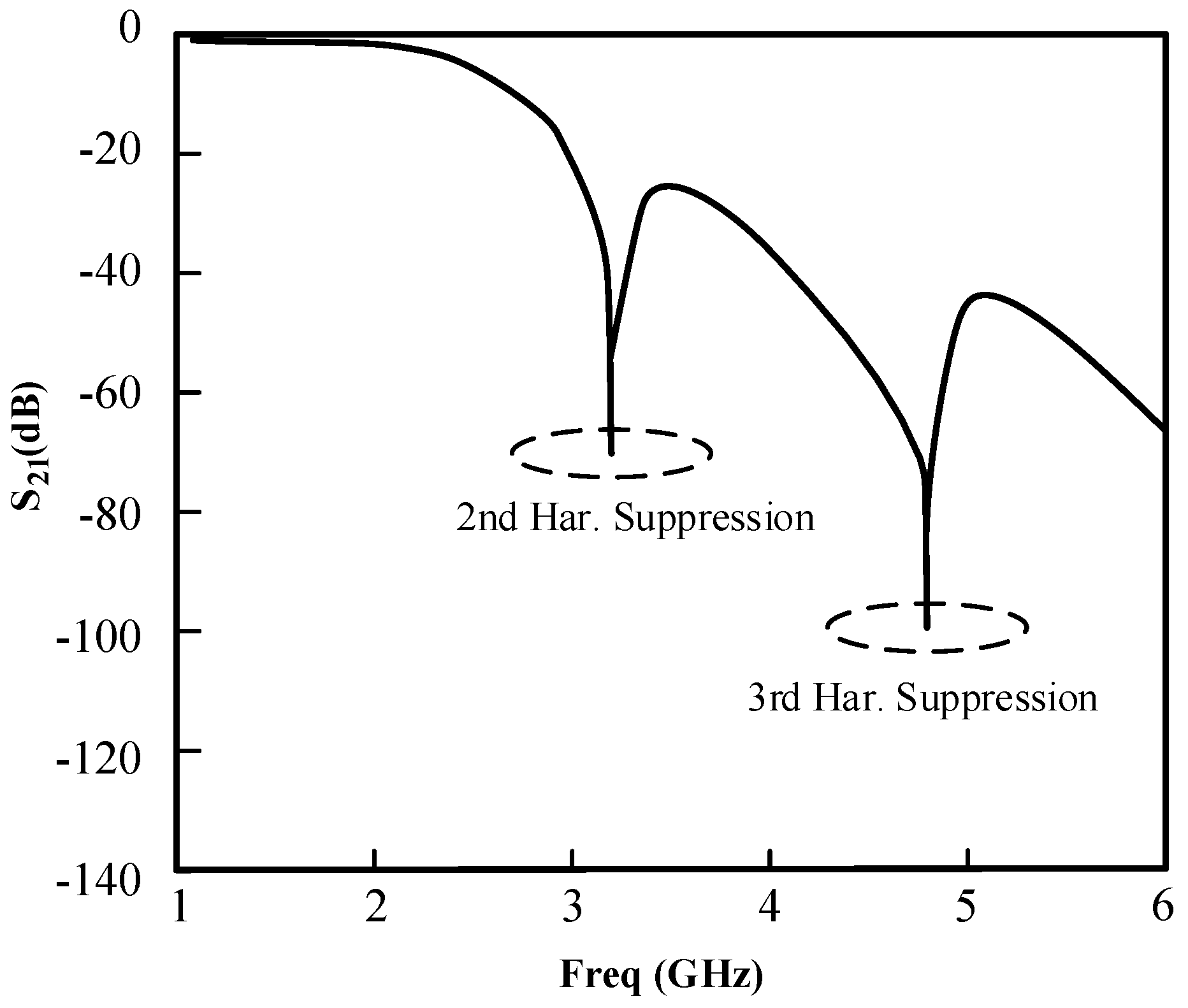
The quasi-elliptic low-pass filtering network synthesized through this topology provides a robust framework for broadband power amplifier design. Within the passband, the network enables continuous impedance transformation from the transistor’s dynamic optimum impedance to the standard load while maintaining low insertion loss, thereby extending the operational bandwidth. Simultaneously, in the stopband, carefully positioned transmission zeros deliver strong attenuation at harmonic frequencies. This arrangement supplies the near-ideal harmonic terminations required for continuous Class-F operation. By integrating these functions into a single network, the design reduces the number of passive components, minimizes parasitic losses, and avoids the impedance-mismatch issues commonly encountered in conventional cascaded architectures. As a result, it offers a high-performance topological basis for enhancing efficiency over wide bandwidths. The proposed power amplifier (PA) operates across a 1.6–2.2 GHz bandwidth. To satisfy the design criteria, a high-order quasi-elliptic low-pass filter (LPF) prototype is integrated into the output matching network (OMN). The OMN is characterized by a passband ripple below 0.5 dB and a cutoff frequency of approximately 2.4 GHz, ensuring minimal insertion loss within the fundamental band. To achieve stringent harmonic suppression and provide optimal harmonic terminations, transmission zeros (TZs) are strategically introduced at 3.2 GHz () and 4.8 GHz (). These TZs yield remarkable simulated rejection levels exceeding 60 dB and 90 dB, respectively, thereby validating the filtering performance and facilitating high-efficiency operation.
To further highlight the advantages of the proposed architecture,
Table 1 compares the performance of this work with recently reported PA designs employing different architecture methods.
3. Circuit Optimization Design
This section will elaborate on the specific design process, circuit implementation, and optimization process based on the above principles. Furthermore, to explicitly account for parasitic effects, the output matching and filtering networks were designed using full-wave electromagnetic simulation. This co-simulation approach inherently captures distributed electromagnetic effects, microstrip discontinuities, and parasitic coupling—the dominant sources of uncertainty in microwave design.
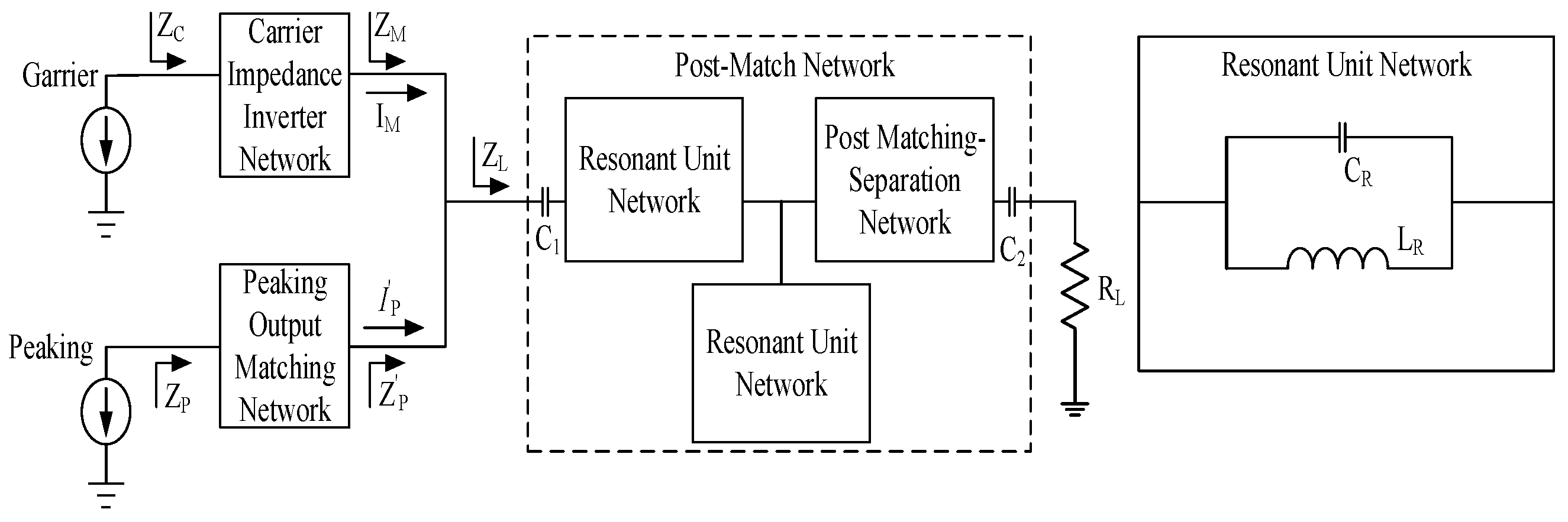
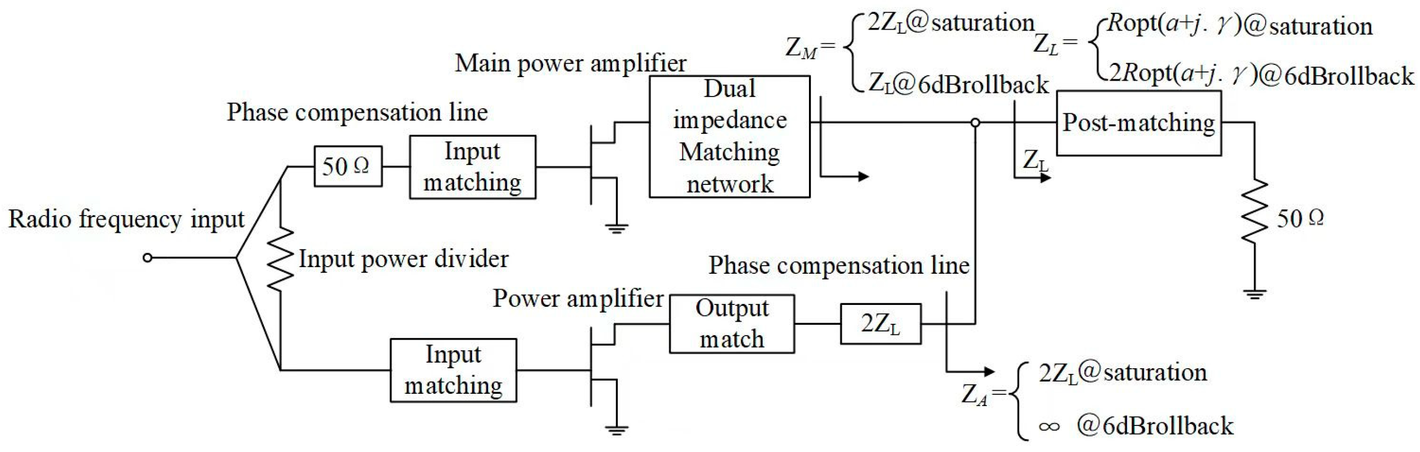
Figure 1 shows the simplified circuit of a traditional Doherty power amplifier (DPA), where all transistors are assumed to be ideal current sources. Its carrier and peaking PA networks achieve core power division and combining through impedance transformation. To meet system linearity requirements, the output terminal of the traditional DPA needs an additional series combination of a “harmonic control unit network + matching network”. However, this separated design has drawbacks: first, it increases circuit topology complexity and debugging difficulty; second, parasitic parameters of multiple components cause extra losses, and signals are prone to reflection at nodes, leading to increased transmission loss. Consequently, this limits efficiency improvement in a wide power dynamic range, making it difficult to meet the needs of high-power scenarios.
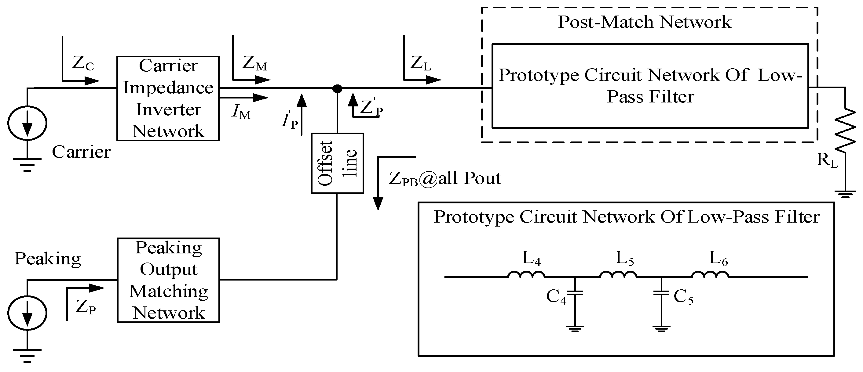
Figure 2 shows the continuous-mode DPA structure proposed in this study, which innovatively integrates a high-order filter prototype into the PA output stage and abandons the traditional “separated harmonic control and matching” architecture. Utilizing the inherent amplitude-frequency characteristics of the high-order filter, it not only achieves accurate impedance matching with the 50 Ω standard load but also effectively suppresses the 2nd and 3rd harmonics—by constructing deep attenuation poles at harmonic frequencies, harmonic energy is reflected back to the PA transistors for dissipation or isolation, thus avoiding harmonic interference and power waste.
denotes the load impedance seen from the transistor drain toward the output matching network. In this work, corresponds to the impedance characteristic of a conventional resonant matching network, whereas represents that of the proposed low-pass-filter-based matching network.
When Z
L = Z
RES, then w = w
0 =
, which is the circuit in
Figure 1. The simplified circuit of a traditional DPA is purely resistive, with extremely narrow bandwidth and poor out-of-band suppression.
When Z
L = Z
LPF, then w
, the circuit in
Figure 2 is wider, and the out-of-band suppression of the series parallel structure is steeper than that of the resonant unit. The Offset line achieves precise phase compensation between the peak branch and the carrier branch, improving the bandwidth of power back-off efficiency and saturation efficiency. The combination of the two results in lower synthesis loss and higher utilization of output power. Furthermore, regarding circuit complexity—as depicted in
Figure 2 and
Figure 3—the conventional standalone architecture generally relies on multiple discrete resonating elements to suppress harmonics at targeted frequencies. By contrast, the proposed integrated low-pass-filter (LPF) prototype attains effective harmonic suppression within a unified network topology, capitalizing on its inherent transmission zeros. Consequently, the need for separate components dedicated solely to harmonic control is entirely removed. This marked reduction in complexity not only shrinks the physical layout but also curtails the parasitic losses that would otherwise be introduced by additional elements, thereby establishing a structural basis for improved efficiency throughout the operating band.
In order to quantitatively evaluate the advantages of the proposed integrated structure in insertion loss and efficiency. According to the standard impedance mismatch theory, the power transfer efficiency
from the transistor drain to the load, for any passive output matching network, can be defined as Equation (12):
In the equation, represents the total radio-frequency (RF) power available at the transistor drain, denotes the effective power delivered to the load, is the optimal conjugate impedance required to achieve maximum power extraction from the transistor, and corresponds to the equivalent impedance looking from the output matching network toward the load at the frequency .
For a conventional resonant matching network, the equivalent impedance
under mismatch conditions can be characterized as the sum of the optimum resistance and a reactive mismatch component:
Consequently, the power transmission coefficient (representing the equivalent insertion loss) for the conventional structure is derived as
In contrast, the proposed integrated matching network leverages the inherent passband characteristics of a low-pass filter (LPF) to maintain the equivalent impedance
such that
This yields an optimized power transmission coefficient:
Within the same frequency band, both satisfy inequality (17):
Meanwhile, the relationship between output power and transmission coefficient also satisfies Formula (18):
Assuming the same DC power consumption and excluding device factors, the efficiency ratio between the two is actually
Here, and denote the drain efficiencies of the power amplifier employing the integrated LPF matching network and the conventional discrete matching network, respectively, at a given frequency . This quantitative derivation demonstrates that the relative efficiency enhancement is fundamentally determined by the term . It follows that at the bandwidth edges, the integrated architecture significantly mitigates the efficiency degradation typically induced by reactance fluctuations in conventional matching networks, thereby ensuring high-efficiency performance across the entire operating frequency range.
Figure 3 presents the complete schematic of the proposed broadband continuous-mode Doherty power amplifier (DPA). The radio-frequency (RF) input signal is split into two symmetrical paths using a Wilkinson power divider. A 50 Ω transmission line is deliberately placed in one input branch to function as a phase-compensation element, ensuring that the signals from the Carrier and Peaking paths reach the output combining node with identical phase. This compensation cancels the phase imbalance introduced by the asymmetric matching topologies employed in the two branches. The Carrier and Peaking amplifiers are biased in Class-AB and Class-C, respectively, enabling active load modulation. In the output stage, the conventional matching networks and separate harmonic traps are replaced by an integrated higher-order low-pass filter (LPF) network. This LPF network simultaneously performs broadband impedance transformation and provides inherent suppression of the 2nd and 3rd harmonics through the creation of deep transmission zeros. As a result, the load impedance
seen by the Carrier amplifier is dynamically modulated over the 1.6–2.2 GHz band, sustaining near-optimum efficiency from deep power back-off up to saturation.
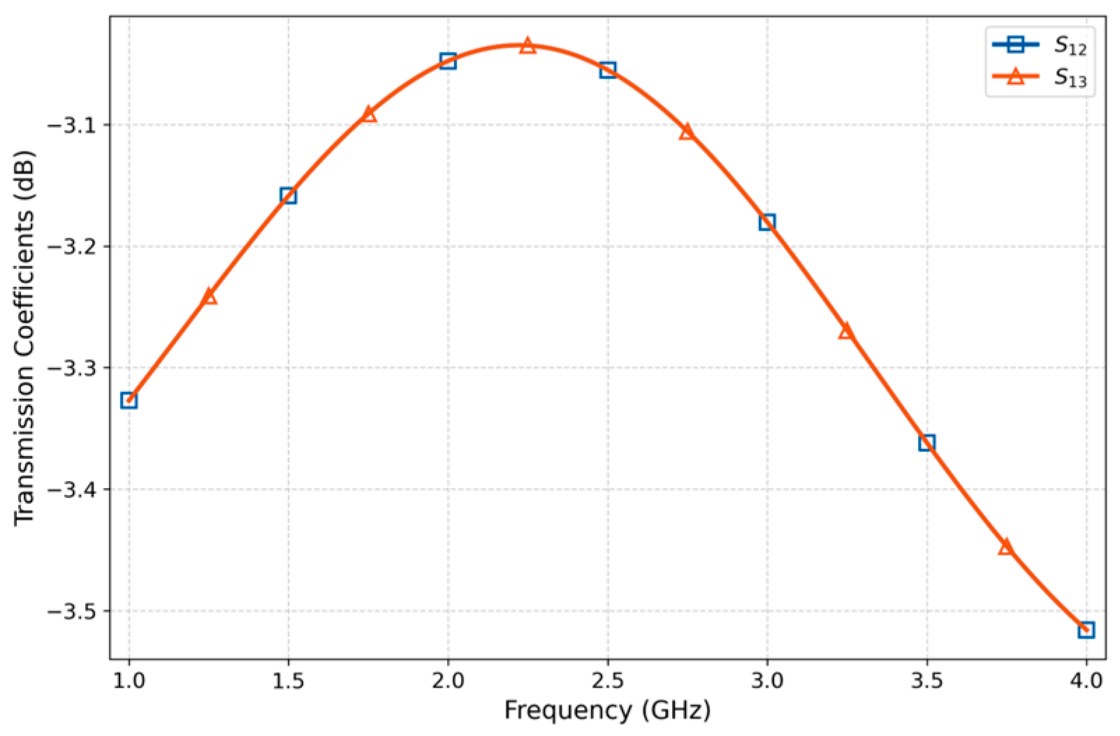
Figure 4 shows that within the working frequency band, the transmission coefficient variation patterns from input port 1 to output port 2 and to output port 3 of the Wilkinson power divider are highly consistent. This indicates that the power divider has excellent amplitude balance, meaning it evenly distributes the signal power to the two output ports, and can relatively equally allocate the input signal power to the two output ports over a wide frequency range.
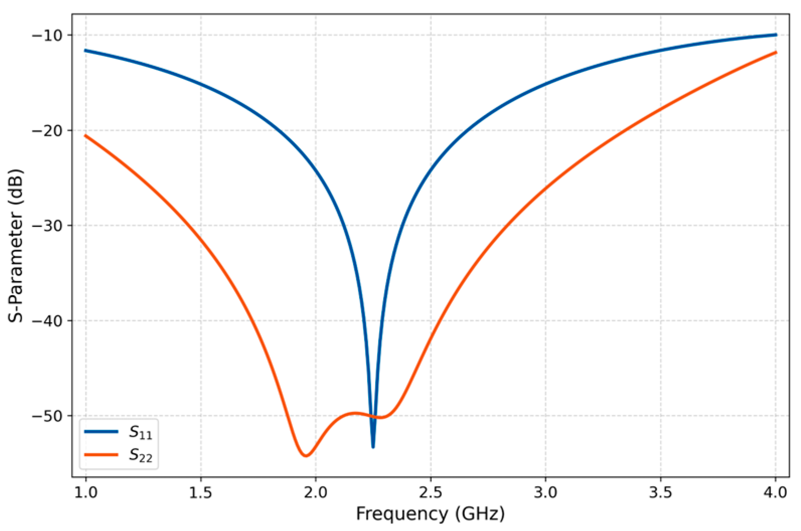
Figure 5 shows that the designed Wilkinson power divider has an insertion loss of approximately −3.1 dB at both ports within the operating frequency band, with a return loss of less than −20 dB, meeting the requirements of this circuit design.
Before designing the specific power amplifier, an IV curve scan was first performed on the CGH40010F device to understand its characteristics. The carrier power amplifier and peak power amplifier were operated in AB-class mode and C-class mode, respectively. Based on the DC simulation results, 28 V was selected as the drain voltage for both the carrier power amplifier and peak power amplifier, and −2.8 V was selected as the gate voltage for the carrier power amplifier. At this point, the drain current is 158 mA, and the transistor operates in deep AB-class mode. The DPA operates in continuity mode. The selection of the gate voltage for the peak amplifier must consider the turn-on threshold of the peak amplifier. The gate voltage of the peak amplifier is generally about 3 V lower than that of the carrier amplifier. Therefore, −6 V is chosen as the gate voltage bias for the peak amplifier in the simulation. To enhance circuit stability, an RC circuit is added to the gate of the device to improve stability.
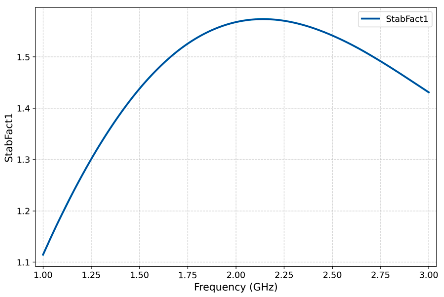
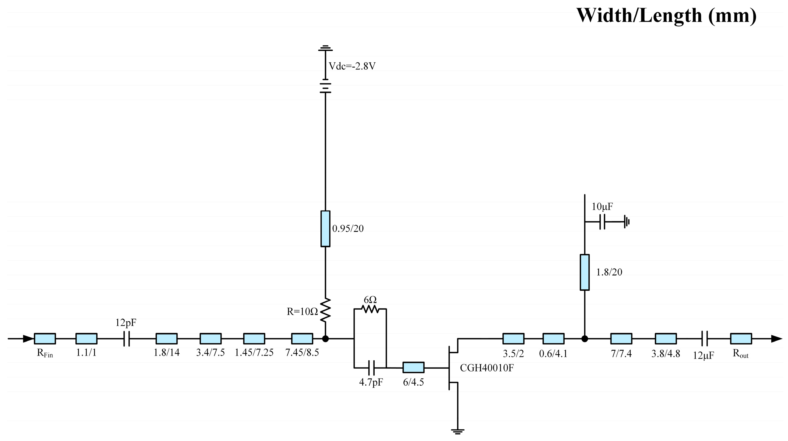
Figure 6 shows that the overall gate RC circuit in this design is maintained at a level greater than 1, effectively enhancing the stability of the amplifier circuit within the operating frequency band and providing good stability assurance for the circuit over a wide frequency range. Based on the simulation results, the values of the stabilizing resistor and capacitor were adjusted, resulting in stabilizing resistor and capacitor values of 6 Ω and 4.7 pF for the carrier amplifier, and 6 Ω and 6.8 pF for the peak amplifier.
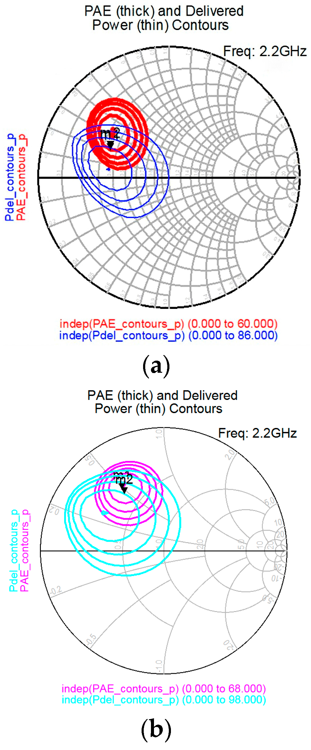
In the design of high-efficiency power amplifiers, systematic impedance optimization is achieved through iterative load-pull simulations.
Figure 7 presents the simulated load-pull impedance contours at 2.2 GHz for (a) saturated and (b) 6 dB power back-off (PBO) conditions. In both plots, thin contours correspond to constant delivered-power (
) levels, while thick contours indicate power-added efficiency (PAE). The overlapping regions of high efficiency and high power define the critical design space for the output matching network. Notably, the upward shift in the optimum impedance toward the inductive region from saturation to back-off illustrates the pronounced influence of transistor parasitic effects near the upper band edge. This observed trajectory directly guides the synthesis of the proposed high-order low-pass filter matching network, which is designed to encompass the impedance requirements of both power modes across the entire 1.6–2.2 GHz band, ensuring a robust performance trade-off between saturation and back-off efficiency. A comparative analysis of these impedance distributions provides essential guidance for the synthesis of the output matching network, enabling performance trade-offs between saturation efficiency and back-off efficiency across different power modes.
Table 2 summarizes the optimal impedances corresponding to the saturated and back-off states at different frequencies. As shown in the table, the real parts of the impedances are relatively similar, while the imaginary parts exhibit significant differences. Specifically, the imaginary part of the impedance in the back-off state is notably larger than that in the saturated state. This discrepancy is primarily attributed to the influence of the transistor parasitic packaging network. At the package reference plane, the impedances obtained through load-pull simulations do not strictly satisfy the theoretical relationship that “the back-off state impedance is twice the saturated state impedance.” Consequently, in practical design, the output matching network must be optimized based on the impedance results obtained from load-pull simulations.
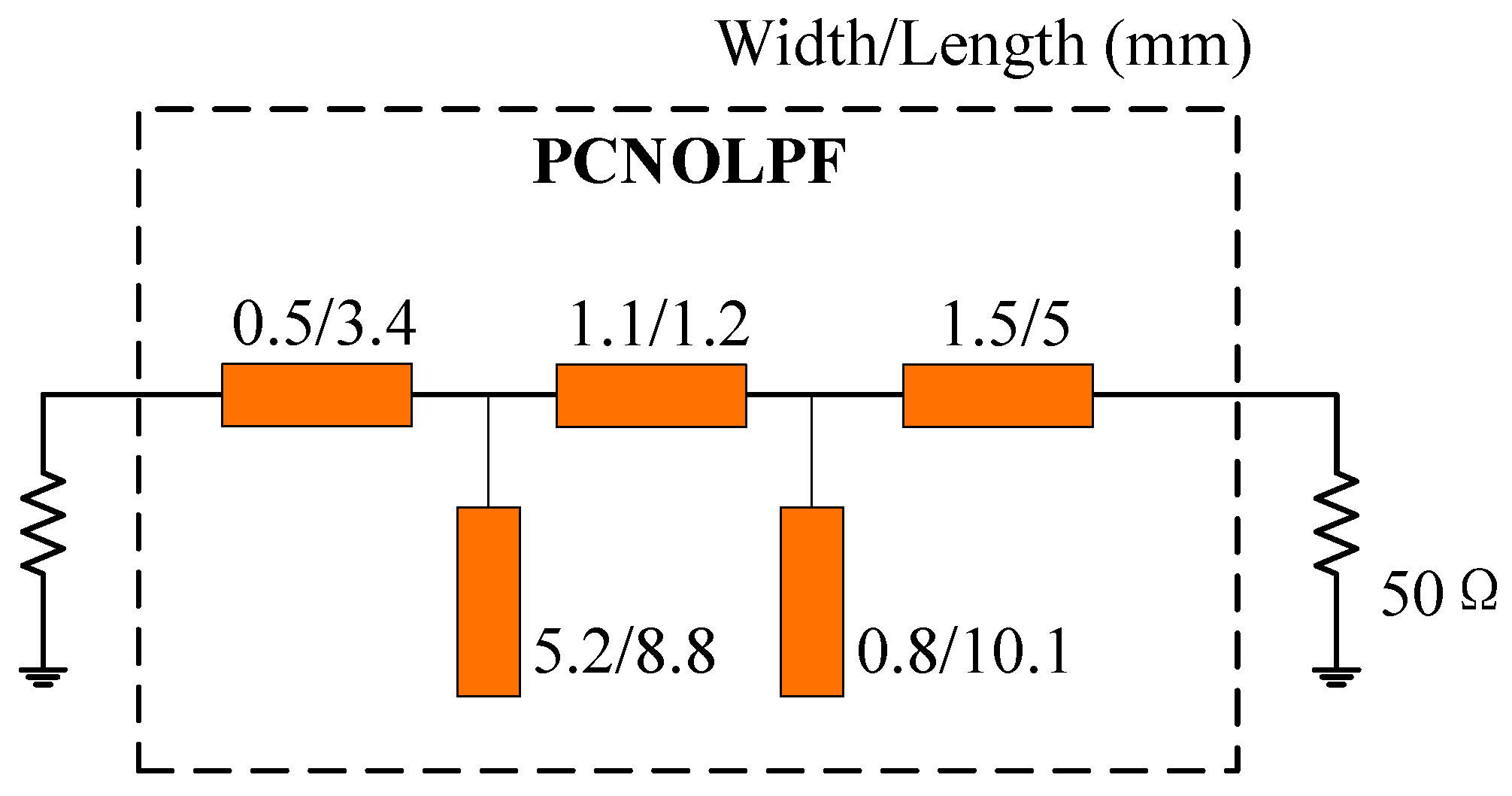
Secondly, the entire circuit needs to be optimized and tuned to achieve suitable output power and efficiency results. After optimization, the entire main power amplifier (PA) topology structure is shown in
Figure 8, including input and output matching networks, ultimately implemented using transmission lines. The impedance and electrical length parameters of each transmission line are obtained at the operating frequency. A Rogers 4350B substrate with a thickness of 20 mil is used. To achieve optimal performance, the circuit parameters of the topology network require fine-tuning. The adjusted post-matching structure is shown in
Figure 9, where the smaller impedance value Z
L is matched to the wireless communication standard of 50 Ω. Impedance grading is employed to mitigate the impact of a single-segment 1/4-wavelength line on the DPA bandwidth.
4. Simulation and Experimental Test Results
This section presents a comprehensive performance evaluation of the proposed broadband continuous-mode Doherty power amplifier. The results are based on both large-signal harmonic balance simulations in ADS and experimental measurements conducted on a fabricated prototype. The amplifier’s performance is benchmarked against prior state-of-the-art works to highlight its advantages. Prior to fabrication, the complete design was rigorously simulated.
The proposed integrated network’s inherent filtering and harmonic-suppression characteristics are validated by the simulated S-parameters of its standalone output matching network, as shown in
Figure 10. Within the fundamental band (1.6–2.2 GHz), the insertion loss (S
21) remains below 0.3 dB, indicating high power transfer efficiency. Moreover, two clearly defined transmission zeros are achieved at approximately 3.2 GHz and 4.8 GHz, corresponding to the second and third harmonics near the lower edge of the design band, with suppression levels of 65 dB and 95 dB, respectively. This intentional placement of transmission zeros confirms the network’s effective harmonic rejection and integrated filtering capability.
Prior to fabrication, the complete design was rigorously simulated.
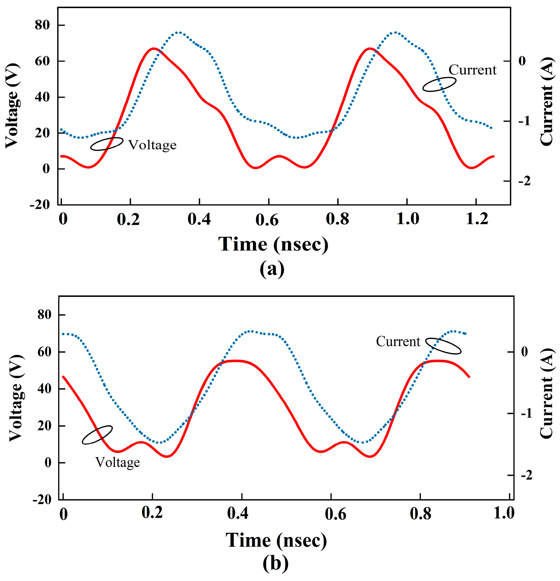
Figure 11 presents the drain current and drain voltage waveforms of the transistor at (a) the lowest frequency (1.6 GHz) and (b) the highest frequency (2.2 GHz) of the operating band. As shown above, the voltage waveform exhibits a distinct flattened peak and a sharply squared valley, demonstrating effective suppression of the second and third harmonics enabled by the integrated filter matching network. Correspondingly, the current waveform closely approximates an ideal half-sinusoidal shape with a conduction angle optimized for high efficiency. It is worth noting that the overlap between the voltage and current waveforms remains consistently low at both band edges, which physically confirms the low power dissipation and high saturated drain efficiency observed in the experimental measurements. Together, these characteristics collectively demonstrate successful realization of continuous Class-F operation across the full 1.6–2.2 GHz bandwidth.
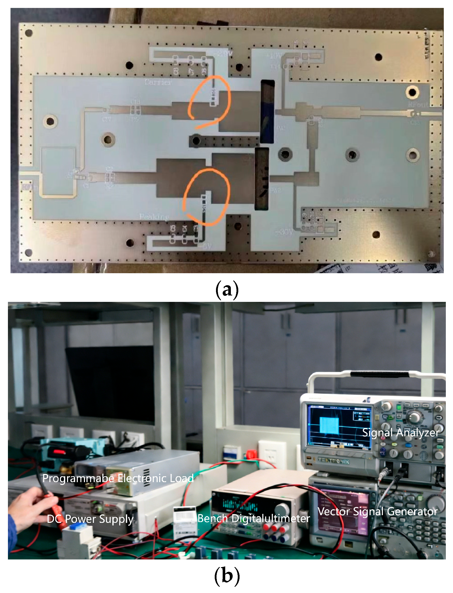
Figure 12a shows the fabricated prototype of the proposed broadband continuous-mode DPA, which employs Cree CGH40010F GaN HEMT mounted on a Rogers 4350B substrate. The DPA is fabricated on a Rogers 4350B substrate with a dielectric constant (
) of 3.66 and a thickness of 0.508 mm (20 mil), and the overall PCB dimensions are 120 mm × 75.4 mm. To clarify the implementation of the matching network, the orange circular markers specifically highlight the short-circuited stubs integrated within the high-order filter-based output networks. These stubs are strategically designed to provide precise harmonic termination for continuous Class-F operation while facilitating broadband impedance transformation. Furthermore,
Figure 12b presents the complete experimental test setup, which includes a vector signal generator (VSG) for input excitation, a signal analyzer for monitoring the output spectrum and power, a DC power supply, and a digital multimeter, thereby comprehensively validating the amplifier’s gain, output power, and drain efficiency and ensuring the accuracy of the measured results.
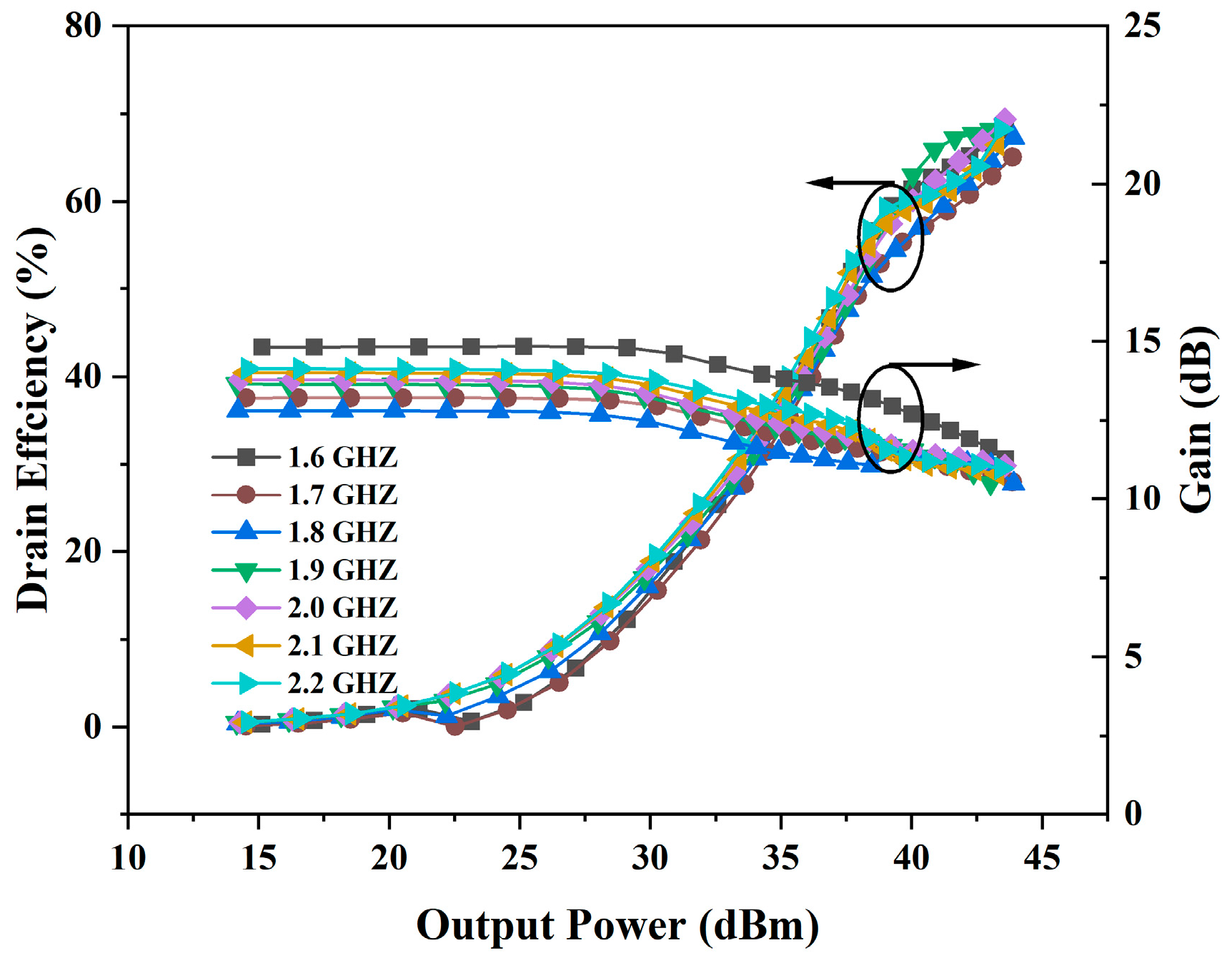
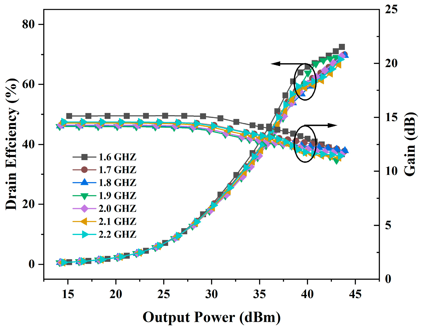
Figure 13 shows the simulation diagram of this design. As can be seen from the figure, within the operating frequency range of 1.6–2.2 GHz, when the output power gradually increases from approximately 15 dBm, the drain efficiency shows an overall upward trend. When the output power reaches approximately 45 dBm, the drain efficiency at nearly all frequencies can approach 70%. Additionally, the gain can reach over 20 dB at low output power levels, and when the output power reaches 45 dBm and enters the saturated state, the gain can exceed 12 dB. At saturation, the simulated drain efficiency of the Doherty amplifier is 70–73%, with an output power of 45 dBm–45.2 dBm and a gain of 11.4 dB–12.8 dB; at a 6 dB power reduction, the drain efficiency is 58.9–64.9%.
Figure 14 shows the experimental data from this study. The drain efficiency reaches 68–72%, and the gain remains above 11.2 dB.
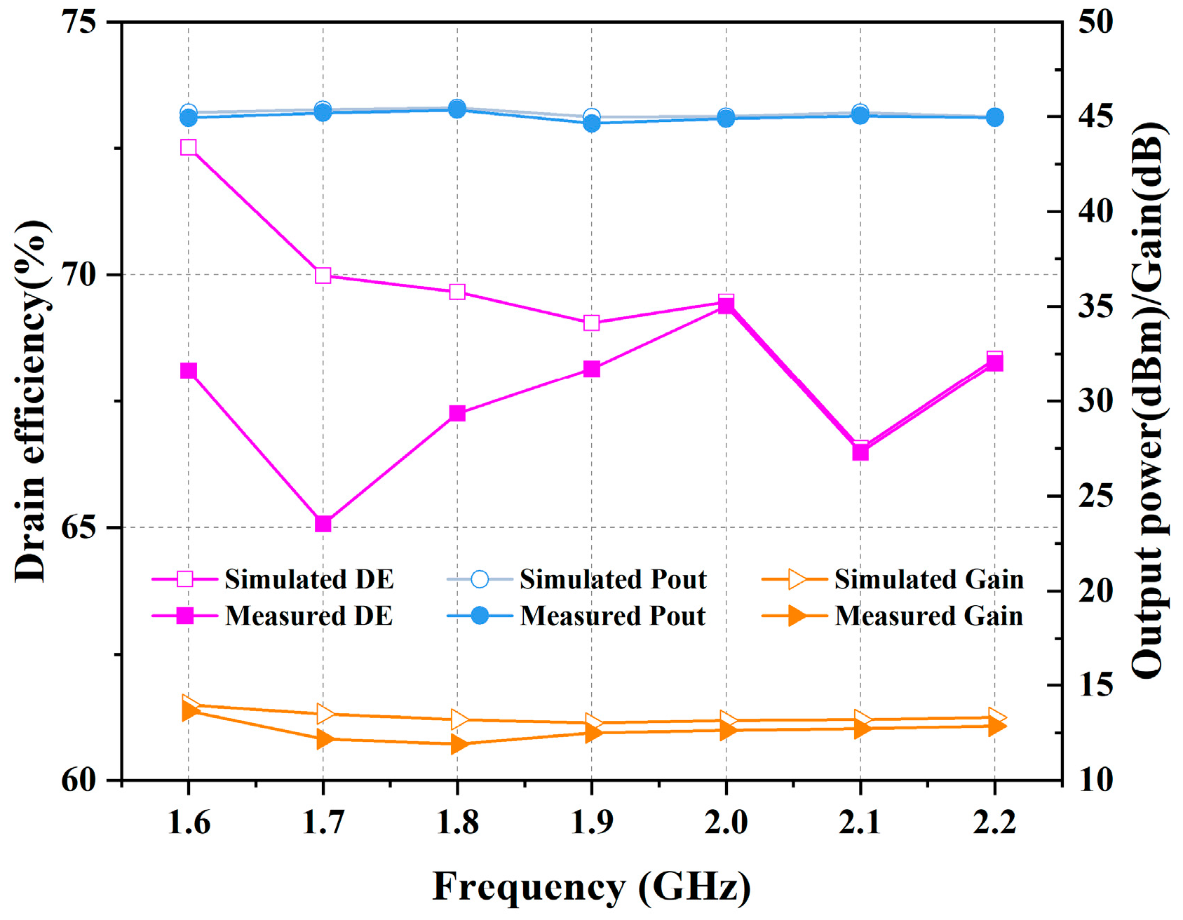
Figure 15 shows the comparison between simulation and experimental results. It indicates that the efficiency fluctuation is approximately 3%, and the gain fluctuation is 0.5 dB, achieving high drain efficiency and gain, and demonstrating excellent wideband power amplification performance. The slight discrepancies observed between the simulated and measured results are primarily attributed to three factors: (i) the inherent modeling limits of the transistor parasitics at harmonic frequencies; (ii) practical implementation losses from SMA connectors and PCB surface roughness; (iii) fabrication tolerances of the microstrip dimensions. Nevertheless, the high degree of consistency in the performance trends validates the robustness of the proposed integrated design. In addition, the high consistency of performance trends validates the robustness of the proposed continuous-mode design and confirms the inherent robustness of the extended impedance space defined by parameters (α, β, γ), which provides a built-in tolerance margin to ensure that small variations in device parasitic or manufacturing tolerances do not significantly reduce performance in the 1.6–2.2 GHz frequency band.
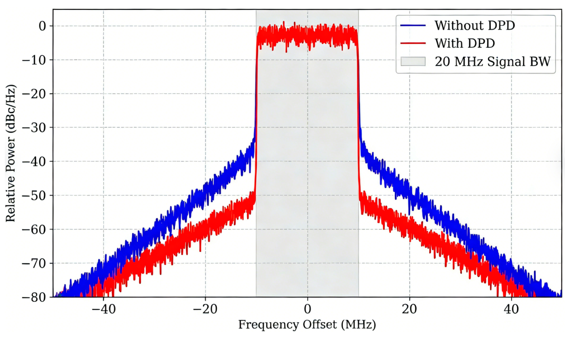
Linearity is a critical metric for evaluating power amplifiers in real-world communication environments. To this end, the proposed continuous-mode Doherty power amplifier (DPA) was characterized using a 20 MHz Long-Term Evolution (LTE) signal with a 7.5 dB peak-to-average power ratio (PAPR).
Figure 16 presents the measured output spectrum at 1.9 GHz, revealing an adjacent channel power ratio (ACPR) of −32.5/−34.2 dBc. These raw linearity metrics, obtained in the absence of digital pre-distortion (DPD), demonstrate that the integrated high-order filtering matching network effectively suppresses spectral regrowth. Given this solid baseline, the application of standard DPD algorithms is anticipated to further enhance the ACPR by 10–15 dB. Such results confirm that the designed amplifier provides sufficient linearization headroom to comply with the rigorous spectral masks required by modern wireless infrastructures.
A comparison of the work in this paper with other related literature on broadband DPAs is presented. As shown in
Table 3, it can be observed that the DPA designed in this paper can ensure high saturated output power and degraded drain efficiency while balancing saturated and degraded outputs to meet the specified criteria. The design is also more reasonable and meets the requirements of practical applications.
5. Conclusions
This design adopts a continuous-wave amplifier model and a broadband impedance inverter structure. It abandons the traditional post-matching structure of “separated harmonic control and matching” and innovatively employs a structure where a high-order filter prototype is directly integrated into the PA output terminal. Simulation results show that within the operating frequency band, the amplifier achieves a saturated drain efficiency of over 68%, a 6 dB back-off efficiency of more than 58.9%, and a gain consistently maintained above 11.2 dB. Experimental measurements further consolidate these trends, demonstrating a saturated drain efficiency of 68–72%, a 6 dB back-off efficiency of 58.9–64.9%, and a saturated output power ranging from 45.1 dBm to 45.2 dBm. Across the 1.6–2.2 GHz frequency range, the gain is consistently maintained above 11.2 dB, peaking at 14.8 dB. The high degree of consistency between the measured and simulated data—with efficiency fluctuations within 3% and gain deviations below 0.5 dB—effectively validates the practical feasibility of the proposed integrated high-order filter matching network. These minor discrepancies are primarily attributed to the parasitic effects of passive components and the inherent dielectric losses of the substrate during fabrication, both of which are considered well within acceptable engineering margins.
The significance of this work is twofold. From a practical perspective, it offers a feasible and efficient design solution for broadband, high-efficiency power amplifiers (PAs)—critical components in modern and next-generation wireless systems such as 5 G/6 G base stations and multi-band software-defined radios. From a theoretical and methodological standpoint, this study demonstrates a strong synergy between continuous-mode PA theory and filter network synthesis, providing a novel and systematic framework for the co-optimization of multiple PA performance metrics.
The integrated high-order filter synthesis method introduced here provides a highly generalizable framework for diverse RF applications. Built on normalized filter prototypes, the design can be scaled to different frequency ranges—including 5 G mid-band and millimeter-wave spectra—by tuning the synthesis parameters according to the required fractional bandwidth. In addition, the integrated filter approach is not limited to the symmetrical Doherty topology presented in this work; it can also be adapted to asymmetrical or multi-way amplifier architectures through appropriate adjustments of the impedance transformation ratios within the filter network. This flexibility makes the proposed co-design method a robust and scalable option for developing future high-efficiency, multi-band communication systems.