1. Introduction
The continuous reduction in feature dimensions in semiconductor manufacturing has led to increasingly demanding overlay requirements [
1]. Advanced logic technologies, three-dimensional integrated circuits, hybrid bonding, backside power delivery networks and high-density memory stacking impose increasingly restrictive overlay budgets throughout the fabrication process [
2,
3,
4,
5,
6,
7]. At these length scales, process-induced wafer distortions can become a significant contribution to the total overlay error.
Wafer distortion may originate from several manufacturing processes, including thin-film deposition, plasma etching, chemical mechanical polishing, thermal annealing and ion implantation [
8,
9,
10,
11,
12,
13]. In particular, non-uniform residual stresses in deposited films can deform the wafer substrate and generate a non-planar free-state wafer geometry. This deformation is commonly characterised through out-of-plane deformation (OPD), wafer bow or wafer shape. Once the wafer is loaded onto a vacuum or electrostatic chuck, the free-state geometry is constrained and the wafer is forced towards a flat configuration. This flattening process generates additional in-plane displacements that may affect the position of previously patterned structures and consequently contribute to overlay error.
It is important to distinguish between the different deformation mechanisms involved in this process. The residual stress of a thin film can generate in-plane strain within the film–substrate system and, consequently, a non-planar wafer shape. By contrast, the present work focuses on the in-plane displacement field generated when that pre-deformed wafer is subsequently flattened against a chuck.
The relationship between thin-film stress and wafer curvature has traditionally been investigated using the Stoney equation and its subsequent extensions [
14,
15,
16,
17,
18,
19]. These approaches are highly valuable for estimating average film stress from global wafer curvature measurements. However, they provide limited information about the local displacement field generated during chucking and are therefore insufficient for directly predicting spatially resolved overlay-relevant distortions in advanced manufacturing processes.
The development of full-wafer optical metrology systems has enabled the acquisition of high-density wafer-shape measurements, thereby motivating the development of models relating measured OPD to in-plane distortion (IPD) [
20,
21]. In this context, Turner and co-workers investigated the relationship between wafer shape and IPD using analytical and numerical approaches [
22,
23,
24]. Proceeding from the force and moment balance between a stressed surface film and the substrate, their analysis yields an in-plane displacement proportional to the gradient of the wafer shape,
, and thereby established the physical connection between wafer-shape gradients and in-plane displacement, together with the relevance of wafer geometry for overlay prediction and feed-forward correction. The quantity returned by this relation is the mid-plane strain implied by the film stress state, and it is linear in the wafer shape; it is therefore distinct from the chucking-induced field defined above.
Subsequent experimental studies demonstrated that wafer geometry measurements could be used to estimate process-induced overlay contributions [
25,
26,
27]. van Dijk et al. further investigated wafer-shape-based feed-forward overlay correction using industrial metrology platforms and scanner measurements [
28]. In these approaches, the measured wafer shape is used as an observable related to the distortion affecting patterned structures. The resulting OPD-to-IPD relationship is therefore understood as a process-dependent mechanical relationship rather than as a direct equivalence between wafer height and in-plane displacement.
Analytical gradient-based models offer an efficient description of the OPD–IPD coupling, particularly for simple geometries and long spatial wavelengths. Nevertheless, models derived from one-dimensional beam assumptions may not fully capture the two-dimensional coupling between orthogonal directions in complex, non-axisymmetric wafer shapes. Jiang et al. proposed an analytical thin-plate framework that extends the applicability of gradient-based descriptions by incorporating two-dimensional coupling effects [
29], and which reduces identically to the gradient model for axisymmetric geometries. Their work represents an important development in the general modelling of wafer-shape-induced IPD, and the present study does not seek to improve upon it. Rather, it addresses a different component of the problem: determining the in-plane displacement field associated with the mechanical flattening of a wafer whose free-state geometry has been measured experimentally. This is consistent with the observation of Jiang et al. that wafer shape alone does not determine the IPD uniquely.
From a mechanical perspective, the problem considered here can be formulated as the response of a thin elastic shell subjected to an imposed out-of-plane flattening condition [
30,
31]. The measured wafer geometry is used to define the initial non-planar configuration, while the chucking condition removes the OPD. The associated membrane–bending coupling then produces an in-plane displacement field. In this formulation, the objective is not to reconstruct the residual stress distribution of the coating or to calculate the in-plane contraction of the film directly. Instead, the objective is to calculate the chucking-induced in-plane response of the wafer from its measured free-state geometry.
A practical requirement of any such prediction is that it be numerically trustworthy, since the input geometry is measured in micrometres while the predicted displacements are of the order of nanometres. Few published methodologies address the numerical conditioning of the prediction process explicitly [
32,
33], despite the accuracy requirements associated with modern overlay budgets.
The objective of this work is therefore to develop a computationally efficient and physically interpretable framework for predicting chucking-induced IPD directly from measured wafer OPD. The wafer is discretised using the Assumed Natural Deviatoric Strain (ANDES) triangular shell element [
34,
35,
36]. This element formulation provides an explicit representation of membrane–bending coupling and is suitable for the analysis of thin-wafer deformation. The constitutive description retains the cubic elastic anisotropy of monocrystalline silicon [
37,
38], whose contribution to the predicted field is quantified in
Section 3.4. The assembled stiffness matrix is partitioned into in-plane and out-of-plane degrees of freedom, allowing the unknown in-plane displacement field to be recovered through static condensation [
39,
40]. In contrast to conventional finite-element workflows built on general-purpose commercial solvers, in which the assembled operator is not exposed, the proposed implementation operates directly on the explicit matrix partitions, providing access to the numerical properties of the condensed system and allowing its condition number to be evaluated [
32,
41].
The proposed methodology accepts measured wafer-shape maps as input, accommodates arbitrary non-axisymmetric geometries and requires only a single factorisation for a given mesh and chuck configuration, after which each measured map is processed by a single back-substitution. It is consequently intended to provide a rapid and reproducible route from measured wafer OPD to the corresponding chucking-induced IPD field, supporting metrology-driven overlay analysis and feed-forward correction workflows. Its sensitivity to metrology noise and its computational cost are quantified in
Section 3.5 and
Section 3.6.
2. Theoretical Formulation
2.1. Problem Definition
The objective of the present work is to predict the IPD generated when a processed silicon wafer is flattened against a lithographic vacuum chuck. In advanced semiconductor manufacturing, wafer geometry is typically characterised through high-density optical metrology measurements performed before and after a given process step [
21,
42]. The difference between both measurements defines the process-induced OPD, which constitutes the primary observable quantity available for feed-forward overlay correction.
Consider a silicon wafer occupying the mid-surface domain
with thickness
h and Cartesian coordinates
defined on the wafer surface.
The measured process-induced deformation is represented by the differential wafer-shape field
where
and
denote the measured OPD geometries immediately before and after the process step, respectively.
The present formulation does not attempt to reconstruct the underlying physical origin of the deformation. Instead, all process-dependent effects, including residual stress, stress gradients, thermal mismatch, material removal, and film non-uniformities, are implicitly contained within the experimentally measured field . Consequently, the prediction framework operates directly on metrology data, requiring no additional information regarding process conditions or material history.
Prior to lithographic exposure, the wafer is mechanically flattened against a reference chuck surface [
23]. This operation removes the measured OPD while simultaneously generating an IPD field through the intrinsic membrane–bending coupling of the wafer structure.
The quantity of interest is therefore the chucking-induced IPD field
which describes the lateral displacement experienced by every point of the wafer surface after chucking. Expressed in Cartesian coordinates, the field can be written as
where
and
denote the displacement components along the
x- and
y-directions, respectively.
These displacements are directly relevant to overlay performance because they modify the position of previously patterned structures with respect to the scanner reference frame [
22]. As illustrated in
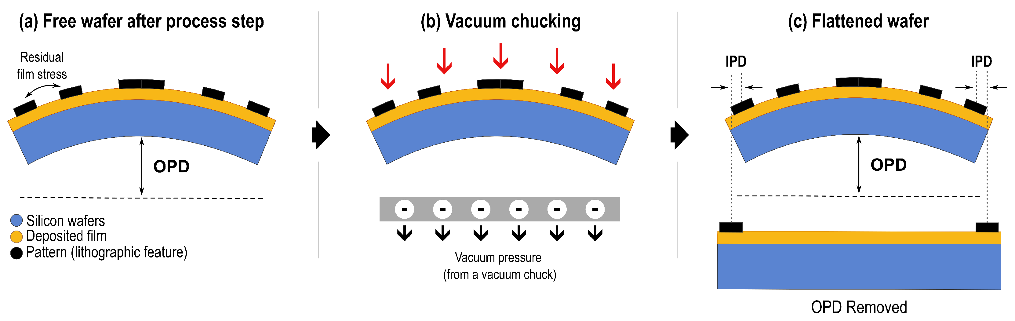
Figure 1, process-induced OPD is removed when the wafer is flattened against the vacuum chuck; however, the associated IPD remains embedded within the substrate, producing the displacement field
that ultimately contributes to overlay error.
2.2. Kinematics of Wafer Flattening
The prediction methodology proposed in this work is based on the observation that the complete deformation state imposed during chucking can be derived directly from the measured differential wafer geometry
. Within the framework of classical thin-plate theory [
30,
43], the deformation of a wafer is fully characterised by the transverse displacement field and the associated rotations of the surface normal. Consequently, once the wafer shape has been measured, the kinematic quantities required to define the chucking boundary conditions can be obtained without any knowledge of the underlying stress field that generated the deformation.
Given the large diameter-to-thickness ratio of standard semiconductor wafers (
for a 300 mm wafer), their mechanical response is well represented by the Kirchhoff–Love hypothesis, which assumes that normals to the undeformed mid-surface remain straight and normal to the deformed surface after deformation [
30,
31,
43]. Under this assumption, the three-dimensional displacement field at any material point of the wafer may be expressed in terms of mid-surface quantities as
where
is the in-plane displacement of the mid-surface,
w is the transverse deflection, and
is the through-thickness coordinate. Transverse shear deformation is neglected and the local orientation of the wafer is completely determined by the gradient of the OPD field.
Equation (
5) implies that the in-plane strain tensor varies linearly through the thickness,
where the membrane strain and curvature tensors are defined as
In the geometrically nonlinear (von Kármán) setting, the membrane strain additionally contains the quadratic rotation term
[
31,
43]. The relative importance of this contribution with respect to the bending-induced surface strain can be estimated by introducing a characteristic deformation amplitude
and lateral wavelength
L, for which
and
. The ratio between both strain contributions then becomes
For the wafers analysed in this work,
μm and
μm, so that the nonlinear membrane term amounts to at most ∼3.5% of the bending-induced strain. The linear kinematics of Equations (
5)–(
7) are therefore adopted throughout, and the small-rotation approximation is fully justified.
During chucking, the wafer is forced to conform to the geometry of the lithographic chuck. Let
denote the out-of-plane geometry of the chuck reference surface expressed in the same coordinate system as the measured wafer shape. Assuming perfect contact and a rigid chuck [
23], the prescribed displacement field required to bring the wafer from its free configuration
to the chuck geometry is
The corresponding rotations of the wafer normal follow directly from the gradient of the imposed displacement field and are therefore given by
where the sign convention follows the right-hand rule adopted for the shell kinematics.
Consequently, the complete out-of-plane kinematic state prescribed at each node of the finite-element model can be expressed as
where
collects the rotational and transverse degrees of freedom associated with the chucking operation.
It should be noted that the chucking condition of Equation (
13) constrains the out-of-plane degrees of freedom only. No in-plane displacement is prescribed at the contact interface: apart from the suppression of the three in-plane rigid-body modes, the mid-surface is free to relax within the plane of the chuck. The formulation therefore represents the frictionless limit, in which the membrane strains generated by flattening relax completely, and the resulting field constitutes an upper bound on the chucking-induced IPD. Any residual adhesion or partial pinning at the wafer–chuck interface, such as that associated with friction at the burl contacts of a vacuum chuck, can only restrict this relaxation and reduce the predicted displacement.
Equation (
13) demonstrates that the entire prediction problem may be parameterised by two measurable geometric quantities: the differential wafer shape
and the chuck reference geometry
. Once these surfaces are known, all kinematic quantities required to define the flattening process follow directly from Equations (
10) and (
11). No assumptions regarding film stress, thermal loading, deposition conditions, material removal mechanisms, or process history are required.
From a mechanical perspective, the chucking-induced IPD problem can therefore be interpreted as the response of a thin elastic shell subjected to the prescribed displacement field of Equation (
13). The membrane strains generated by this imposed flattening are responsible for the in-plane displacement field that ultimately contributes to overlay error. The following sections develop the constitutive and finite-element framework used to recover this response.
2.3. Membrane–Bending Coupling
Before introducing the discrete formulation, it is instructive to examine the continuum origin of the OPD-to-IPD coupling. Integration of the through-thickness stress distribution associated with Equation (
6) yields the classical shell stress resultants [
43],
where
and
collect the membrane forces and bending moments, and the extensional, coupling and bending stiffness matrices are obtained from the plane-stress constitutive matrix
of Equation (
25) as
The corresponding elastic energy functional of the shell reads
For a homogeneous plate referenced at its geometric mid-surface, the material coupling matrix vanishes,
, and the membrane and bending problems of the idealised flat plate decouple. The coupling responsible for chucking-induced IPD is instead of geometric nature: the wafer occupies an initially non-planar configuration described by
, and the imposed flattening transports material points along this curved reference surface. In the discrete shell model, where the curved wafer is represented by an assembly of flat triangular facets with distinct local orientations, this geometric coupling appears naturally as the off-diagonal stiffness block
linking in-plane and out-of-plane degrees of freedom [
35].
An important consequence of Equation (
5) concerns the overlay-relevant displacement. In the chucked configuration the wafer is flat,
, and therefore the in-plane displacement of the patterned surface coincides with that of the mid-surface. Since overlay compares two chucked states, before and after processing, the quantity governing overlay error is precisely the mid-surface field
recovered by the present formulation.
This observation also clarifies the relation with the classical gradient model of the literature [
24,
28], which returns the mid-plane strain retained after chucking,
The factor
originates from a one-dimensional beam equilibrium in which the measured shape is assumed to be generated by the integrated stress of a thin surface film; the mid-plane membrane strain accumulated during processing is then retained after chucking [
14,
29].
2.4. Elastic Behaviour of Silicon
The mechanical response of monocrystalline silicon is inherently anisotropic. Unlike isotropic engineering materials, whose elastic properties are independent of direction, the stiffness of silicon varies with crystallographic orientation due to its diamond-cubic crystal structure [
37]. Although isotropic approximations are frequently adopted in wafer-scale mechanical simulations, the accuracy requirements associated with modern overlay budgets motivate a more rigorous constitutive description [
44].
Silicon belongs to the cubic crystal system and therefore exhibits three independent elastic stiffness constants [
38,
45,
46,
47,
48],
which completely define the fourth-order elasticity tensor. The resulting material behaviour departs significantly from isotropy, as evidenced by the Zener anisotropy ratio [
49]
where a value of unity corresponds to an isotropic solid. The measured value indicates that the shear response of silicon differs substantially from the equivalent isotropic approximation.
While the stiffness constants
relate strains to stresses,
, directional engineering properties are more conveniently expressed in terms of the elastic compliance coefficients
, which describe the inverse relation
. For cubic symmetry, the compliance coefficients follow directly from the stiffness constants as [
45]
which, for the constants of Equation (
18), yield
Physically, represents the longitudinal strain produced by a unit uniaxial stress applied along a crystal axis, the accompanying transverse contraction (responsible for the Poisson effect), and the shear strain produced by a unit shear stress on the cube faces.
Most semiconductor wafers are manufactured with a (001) surface orientation. For this crystallographic plane, projection of the cubic elasticity tensor onto the wafer surface yields an orthotropic in-plane constitutive behaviour when expressed in the
–
reference frame [
37]. Although the elastic response remains identical along the two principal crystal directions, the stiffness differs significantly from that observed along intermediate orientations such as
. The in-plane orientation
is referred to the physical wafer through the orientation notch, which for (001) wafers is aligned with the
direction according to SEMI M1 [
50].
This effect can be quantified through the directional Young’s modulus
where
denotes the in-plane orientation measured from the
crystal axis. The corresponding in-plane Poisson’s ratio, relating the transverse in-plane contraction to the longitudinal extension for a uniaxial load applied along
, is [
37,
45]
For the (001) wafer plane, Equations (
22) and (
23) predict
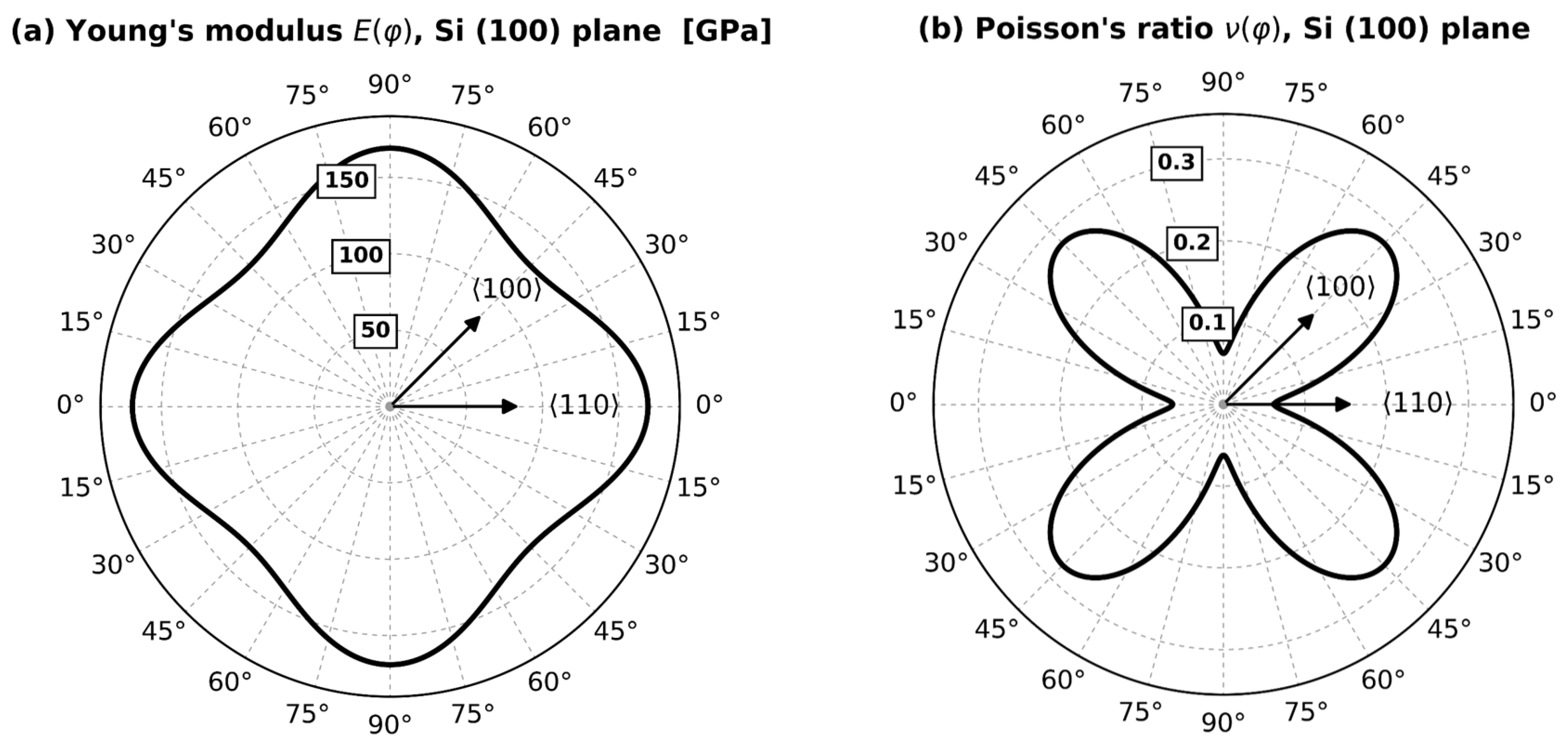
representing a variation of approximately 30% in stiffness and of more than a factor of four in the Poisson response between both directions. The complete directional dependence is illustrated in
Figure 2, where the characteristic four-fold symmetry of the (100) plane is clearly visible: the Young’s modulus attains its maxima along the
directions, whereas the Poisson’s ratio exhibits the opposite behaviour, with maxima along
.
For the present application, the most relevant consequence of anisotropy is the modification of the membrane stiffness and membrane-bending coupling that govern the generation of chucking-induced IPD. Since the proposed formulation obtains in-plane displacements directly from the elastic response of the wafer, directional variations in stiffness are expected to influence the predicted displacement field, particularly for non-axisymmetric deformation patterns.
Under plane-stress conditions (
), the reduced in-plane constitutive matrix adopted in the present work is
For finite elements whose local coordinate system is not aligned with the crystal axes, the constitutive matrix must be transformed to the local element reference frame prior to stiffness evaluation. Under plane-stress conditions, the transformed constitutive matrix is obtained using the standard Voigt transformation [
51]
where
denotes the angle between the local element axes and the crystallographic
direction. The stress and strain transformation matrices are
with
This transformation preserves the physical constitutive response while expressing it in the local coordinate system of each finite element. The rotated constitutive matrix is subsequently used to compute the element stiffness matrix following the standard orthotropic finite-element formulation [
43].
2.5. Shell Finite Element Formulation
Once the chucking kinematics have been defined through the prescribed displacement field of Equation (
13), the prediction of chucking-induced IPD reduces to the solution of a linear elastic boundary-value problem [
52,
53]. The wafer is modelled as a thin silicon shell occupying the domain
and discretised by means of finite elements.
The finite-element implementation adopted in this work is based on the Assumed Natural Deviatoric Strain (ANDES) formulation originally developed by Felippa and Militello [
34,
35,
36]. The ANDES family combines the advantages of assumed-strain methods with an explicit decomposition of the element stiffness into basic and higher-order contributions, resulting in low mesh-distortion sensitivity, accurate bending-energy representation, and excellent membrane–bending coupling characteristics. Its formulation derives from the free-formulation lineage of triangular membrane elements with drilling degrees of freedom [
54,
55], whose performance was later characterised systematically within the finite-element template framework [
56,
57]. Compared with classical three-node plate bending triangles [
58], the ANDES bending triangle provides an improved representation of the bending energy on unstructured meshes.
The choice of the ANDES element is particularly attractive for wafer-level deformation analysis because circular wafer geometries are naturally represented through unstructured triangular meshes. Furthermore, the chucking-induced IPD problem is governed by subtle membrane strains generated during wafer flattening, requiring a shell formulation capable of accurately capturing both membrane and bending effects over arbitrary mesh topologies.
Each node possesses six degrees of freedom,
where
u and
v denote the IPD components,
w is the transverse displacement,
and
are the shell rotations, and
is the drilling rotation associated with the shell normal [
54,
57].
For an individual shell element occupying the domain
, the elastic strain energy may be written as
where
denotes the generalized shell strain vector and
is the constitutive matrix describing the elastic behaviour of silicon.
The strain field is interpolated from the nodal degrees of freedom through
where
is the strain–displacement matrix and
contains the element nodal degrees of freedom.
Application of the principle of minimum potential energy yields the classical finite-element stiffness matrix [
51,
52]
Within the ANDES framework, the strain field is decomposed into a basic constant-strain contribution and a higher-order deviatoric component. Accordingly, the element stiffness matrix may be expressed as
where
represents the basic stiffness associated with the constant-stress state, while
accounts for the higher-order deformation modes introduced through the assumed natural deviatoric strain interpolation [
34].
The higher-order contribution is obtained from
where
denotes the deviatoric strain interpolation matrix. This decomposition is a defining feature of the ANDES methodology and is responsible for its favourable numerical performance in bending-dominated problems and distorted triangular meshes [
34,
35,
36].
Assembly of all element contributions yields the global equilibrium system
where
is the assembled global stiffness matrix,
collects all nodal degrees of freedom, and
is the global force vector.
In the present application no external mechanical loads are necessary. The deformation is generated exclusively through the prescribed chucking kinematics introduced in
Section 2.2. Consequently, the global displacement vector is naturally partitioned into free and prescribed degrees of freedom,
where
contains the unknown in-plane degrees of freedom and
contains the prescribed OPD state defined by Equation (
13).
The corresponding partitioned equilibrium equations become
where
contains the pressure load required to enforce the prescribed chucking deformation.
Equation (
36) constitutes the starting point for the static-condensation procedure used to recover the chucking-induced IPD field. The partitioning strategy is particularly advantageous because the complete OPD state is known a priori from metrology measurements, allowing the unknown in-plane response to be obtained directly from the coupling between the two subspaces. The resulting formulation is developed in the following section.
2.6. Static Condensation Framework
Using the partitioned equilibrium equations introduced in Equation (
36), the chucking-induced IPD field may be recovered directly from the prescribed OPD state by means of the classical static-condensation procedure [
39,
40,
52].
For the present problem, the global equilibrium equations can be written as
where
contains the unknown in-plane degrees of freedom and drilling rotations, while
contains the prescribed OPD state obtained from Equation (
13).
Since no external in-plane loads are applied during chucking,
The first block row of Equation (
37) therefore reduces to
Provided that the membrane stiffness matrix
is nonsingular after elimination of rigid-body modes, the unknown in-plane response follows directly as
which constitutes the fundamental equation of the proposed methodology.
Equation (
41) establishes a direct mechanical transformation between the experimentally measured wafer geometry and the resulting chucking-induced IPD field. Unlike conventional finite-element workflows, the complete solution does not require recovery of the full displacement vector. Instead, only the membrane subsystem and the membrane–bending coupling operator participate in the final computation.
For convenience, the transformation may be written in operator form by introducing
which allows Equation (
41) to be expressed as
The matrix
may be interpreted as an OPD-to-IPD transfer operator. For a given wafer geometry, material model and chuck configuration,
completely characterises the mechanical mapping between the prescribed OPD state and the resulting IPD field. In particular, since Equation (
43) is linear, the response to any measured wafer shape may be expressed as the superposition of the responses to a basis of elementary shape modes (for instance, Zernike polynomials), so that the columns of
restricted to such a basis constitute a complete modal characterisation of the OPD-to-IPD conversion for a given wafer and chuck configuration.
The physical interpretation of Equation (
43) is particularly revealing. The prescribed chucking deformation
acts as a geometric excitation that is projected through the coupling block
into an equivalent membrane loading. The membrane subsystem
subsequently determines the in-plane displacement field required to restore equilibrium. Consequently, the complete OPD-to-IPD transformation is governed entirely by the membrane–bending coupling embedded within the shell formulation.
2.7. Numerical Reliability Assessment
A distinguishing feature of the proposed formulation is that the complete condensed system remains explicitly available to the user. Consequently, the numerical reliability of the OPD-to-IPD transformation can be quantified directly from the properties of the membrane subsystem [
32,
33].
The sensitivity of the solution to perturbations is characterised through the condition number of the condensed matrix [
41],
which measures the amplification of numerical errors during the solution process. For finite-element operators, the magnitude of
is governed by the element size, the material contrast and the polynomial order of the discretisation [
59,
60].
For symmetric positive-definite systems, the condition number may be obtained from the spectral decomposition of
. Equivalently, using the singular value decomposition [
41,
61],
the condition number becomes
where
and
are the largest and smallest singular values, respectively.
The condition number provides an upper bound on the sensitivity of the computed IPD field to perturbations in the condensed equilibrium equations [
32]. Specifically,
where
The perturbation
in Equation (
47) admits a direct metrological interpretation: any uncertainty
in the measured wafer shape propagates linearly through the coupling operator,
, so that the bound simultaneously quantifies the amplification of numerical rounding, interpolation error and measurement noise. The condition number therefore connects the accuracy specification of the metrology system [
62] with the achievable accuracy of the predicted IPD field.
In addition to its mathematical interpretation, the condition number provides a practical estimate of the numerical precision retained during the solution process. Assuming IEEE double-precision arithmetic, the approximate number of significant decimal digits lost is [
32,
33]
while the number of remaining reliable digits is approximately
For example, a condition number of implies the loss of approximately six decimal digits, whereas a condition number of reduces the effective numerical precision to roughly four significant digits.
3. Application to Measured Wafer Geometries
The objective of the proposed methodology is the prediction of chucking-induced IPD from experimentally measured wafer geometries representative of those encountered in semiconductor manufacturing environments.
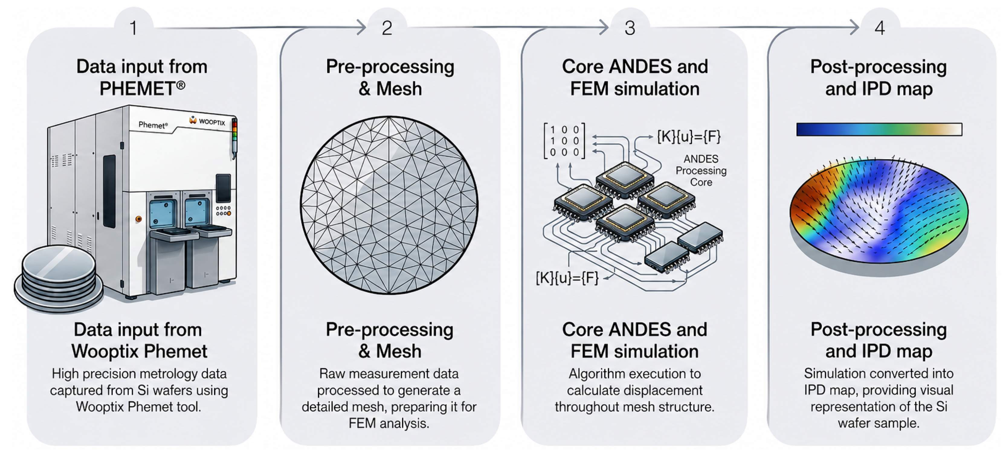
This section evaluates the proposed framework using real wafer-shape measurements acquired through industrial optical metrology. The complete workflow is illustrated in
Figure 3. Starting from the measured wafer geometry, the OPD field is projected onto a modal basis and evaluated at the finite element nodes, and transformed into the prescribed chucking state defined in
Section 2.2. The resulting deformation state is then processed through the shell-based static-condensation framework in order to recover the corresponding IPD field. Finally, the numerical conditioning of the condensed system is evaluated to quantify the reliability of the prediction.
The first step of this workflow deserves to be stated explicitly, since the measured map and the mesh are defined on unrelated supports. The metrology delivers the wafer geometry as a dense set of samples on a regular grid of 65 µm pitch, comprising approximately
points over the full 300 mm aperture, whereas the analysis is carried out on an unstructured triangular mesh whose positions bear no relation to the sampling grid. Rather than interpolating the measurement pointwise, a modal surface is fitted to it in a least-squares sense over the full set of valid samples and the resulting analytic function is evaluated at the nodal coordinates. Over the wafer aperture of radius
R, with
, the fitted geometry is written as
where the modes are indexed by radial order
n and azimuthal frequency
m,
with radial polynomials
and the normalisation
for
and
otherwise, chosen so that
over the aperture. The coefficients follow from
where
collects the measured heights and
the modes evaluated at the sample coordinates. The expansion is truncated at radial order
, giving
modes, and the system is solved by singular value decomposition. Samples falling within the edge exclusion zone are omitted from the fit.
Three considerations motivate this choice over pointwise interpolation. The governing one is that the formulation does not consume the measured height itself but its gradient: the geometric membrane–bending coupling enters through the local orientation of each facet, so the prediction is determined entirely by
. A pointwise scheme transfers nodal values and leaves the gradient to be recovered by differentiating the element shape functions, which on linear triangles yields an element-wise constant gradient, discontinuous across element edges and sensitive to the high-frequency content of the measurement. The fitted surface of Equation (
51) is smooth, and its gradient is available in closed form and evaluated analytically at each node, so the quantity the model depends on is obtained without numerical differentiation of the measurement.
The second consideration is that the nodal coordinates do not coincide with sample positions. Consequently, any pointwise transfer would require a local interpolation rule between neighbouring samples and would make the prescribed geometry depend on the mesh layout. Evaluating a global analytic function removes this dependence, allowing the same fitted surface to be evaluated on any mesh.
The third consideration is that the projection of Equation (
54) is an approximation rather than an interpolation. It retains only the component of the measurement lying in the span of the 66 modes and discards the orthogonal remainder. Since the sample count exceeds the mode count by five orders of magnitude, the system is strongly overdetermined and the projection is well conditioned. The consequences for the propagation of measurement uncertainty are examined in
Section 3.5.
3.1. Experimental Wafer Dataset
The wafer geometries employed in this study were acquired using the Phemet
® wafer metrology platform (Wooptix, La Laguna, Spain), a full-field optical metrology system based on Wavefront Phase Imaging (WFPI) technology [
42,
62]. Unlike conventional scanning approaches [
63,
64], WFPI reconstructs the complete wafer surface from a single acquisition, providing dense topographic information over the entire wafer aperture while maintaining high measurement throughput.
Because the technique reconstructs the complete wafer aperture in a single acquisition, the measured maps contain the orientation notch, which provides the reference required to register the crystal frame of
Section 2.4 with the coordinate system of the model.
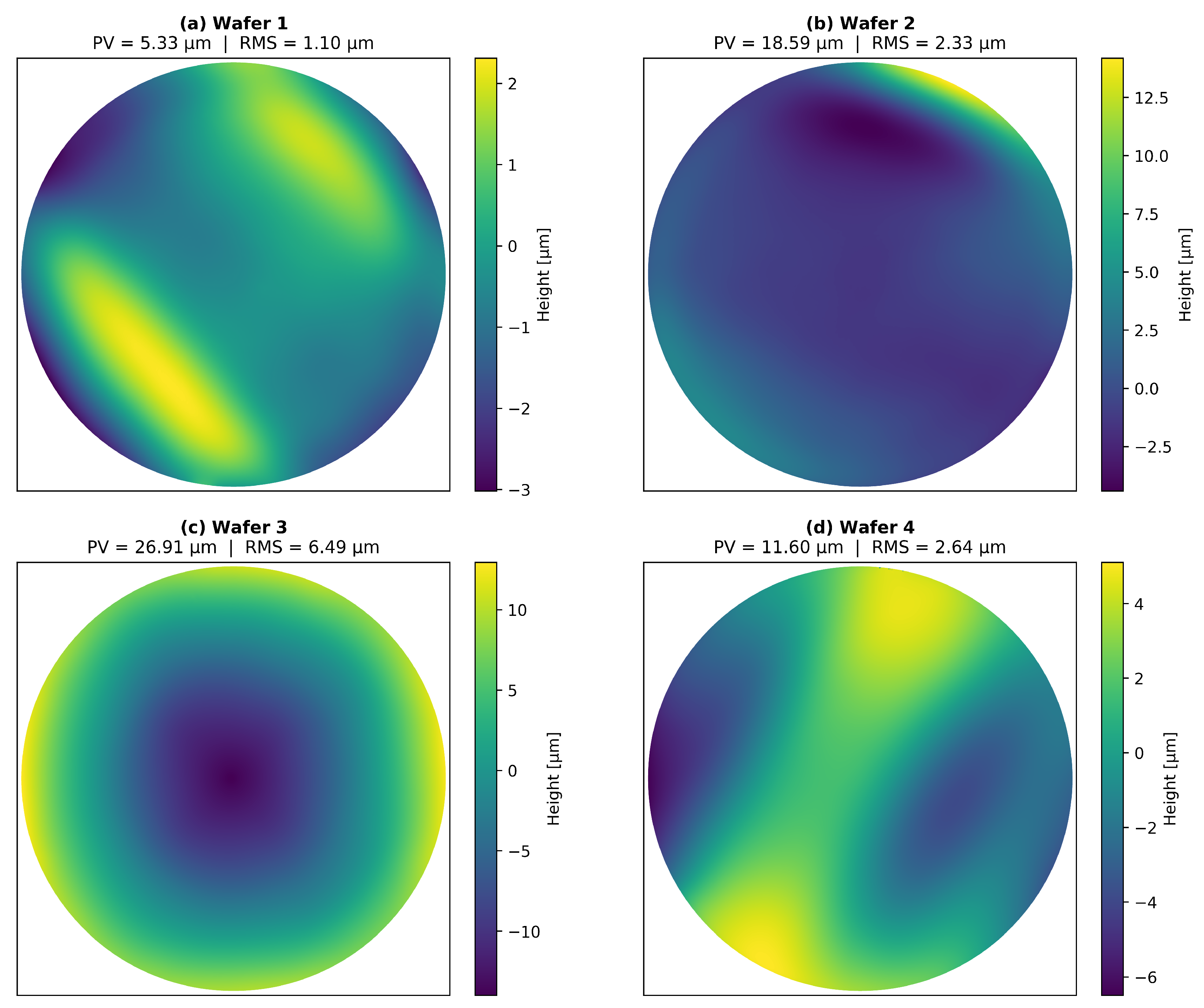
Figure 4 presents the measured OPD maps used throughout this work. The selected wafers cover peak-to-valley (PV) values ranging from approximately 5 µm to 27 µm and include both nearly flat wafers and highly bowed or warped samples, providing a challenging benchmark for OPD-to-IPD prediction.
3.2. Predicted IPD Fields
The proposed static-condensation framework was applied independently to each wafer geometry shown in
Figure 4. The resulting solutions provide the complete chucking-induced displacement field
over the wafer surface.
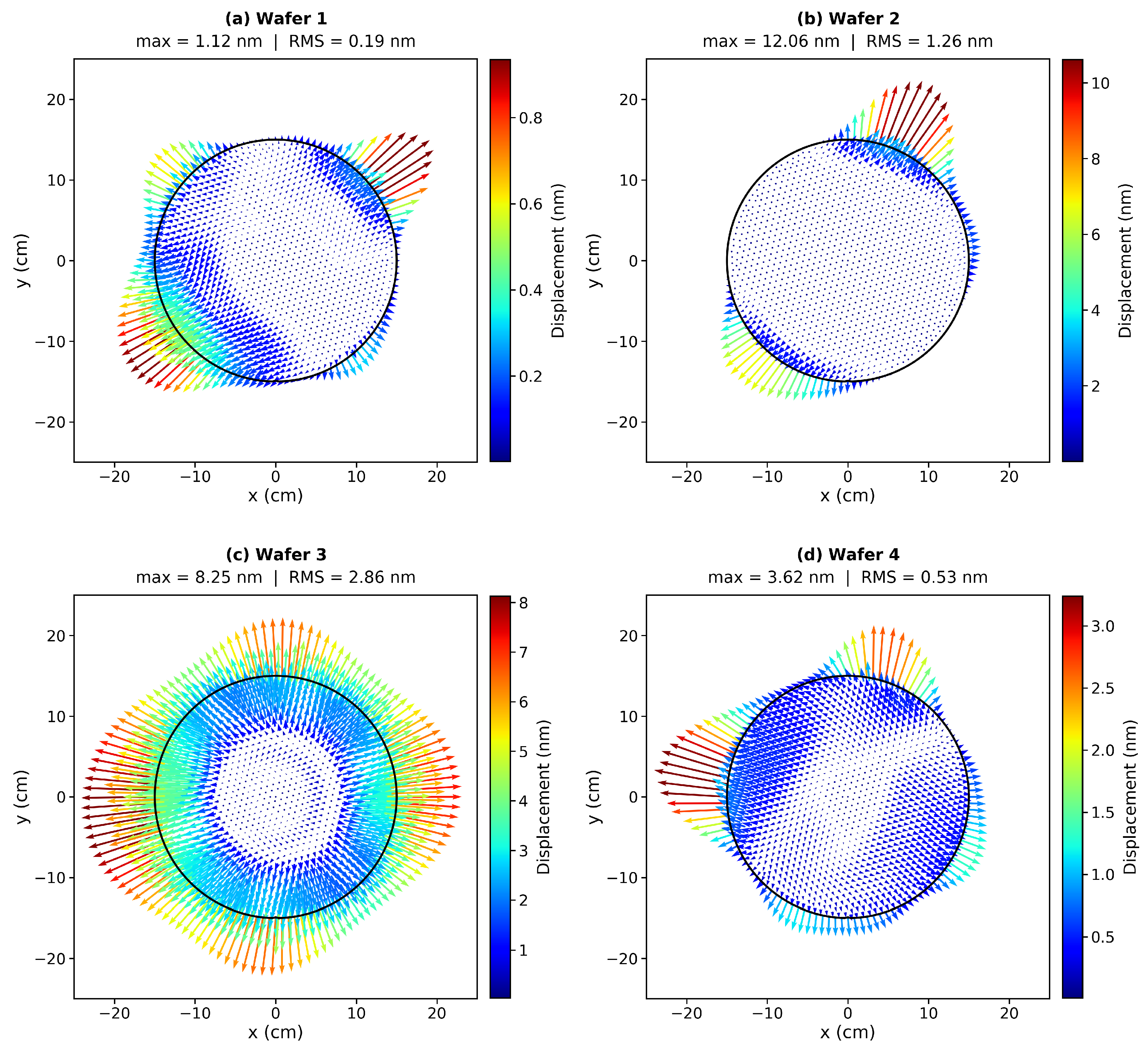
Figure 5 presents the predicted IPD fields for the four analysed wafers. Each map displays the displacement vectors
predicted, with arrow orientation indicating the local direction of the distortion and colour encoding its magnitude. Note that the displacement vectors are strongly exaggerated for visualisation purposes; the actual displacement magnitudes remain in the nanometre range, several orders of magnitude smaller than the wafer diameter. The solid black circle denotes the undeformed wafer edge, and an independent colour scale is used for each wafer owing to the large spread of distortion amplitudes across the dataset.
The four wafers develop clearly different IPD signatures, directly inherited from the spatial structure of their measured OPD.
Wafer 1 (
Figure 5a) exhibits the smallest distortion level of the dataset, with a maximum predicted displacement of approximately 1.12 nm. Its saddle-like free-form geometry produces a markedly non-axisymmetric displacement pattern, in which the largest displacements concentrate along two diagonally opposed edge sectors while the wafer centre remains essentially undistorted. The strong tangential (non-radial) component of this field is characteristic of low-order astigmatic wafer shapes.
Wafer 2 (
Figure 5b) develops the largest predicted distortion of the dataset, with peak displacements of approximately 12.06 nm localised in two nearly antipodal edge regions coinciding with the pronounced local depression observed in the measured geometry. Away from these regions the displacement field decays rapidly towards the wafer interior, confirming that localised warpage generates equally localised IPD rather than a global signature [
20].
Wafer 3 (
Figure 5c) displays the almost purely radial, axisymmetric displacement field expected for a bowl-shaped wafer. The displacement magnitude increases monotonically from the centre towards the edge, where it reaches approximately 8.25 nm. This behaviour is consistent with the geometric mechanism governing the flattening of a spherical cap, which produces a purely radial membrane displacement that accumulates towards the wafer edge [
24].
Finally, Wafer 4 (
Figure 5d) presents an intermediate situation, combining a dominant lobe of distortion reaching approximately 3.62 nm on the left-hand edge with a weaker free-form background over the remainder of the surface, mirroring the long-wavelength asymmetry of its measured OPD map.
Two general observations emerge from these results. First, the IPD fields reported here are normalised with respect to the wafer centre, which is taken as the origin of the displacement field; any other reference point may be adopted without altering the physical content of the solution, since only relative displacements between locations are overlay-relevant. Second, and most importantly, the ranking of the wafers in terms of IPD does not follow their ranking in terms of OPD amplitude. Wafer 3 exhibits the largest OPD (PV = 26.91 µm) but only the second-largest IPD, whereas Wafer 2, with a substantially smaller PV of 18.59 µm, generates the largest of the dataset. This demonstrates that global shape metrics alone are insufficient predictors of overlay-relevant distortion, in agreement with the conclusions drawn from wafer-geometry-based overlay studies [
21,
25,
29].
3.3. Discretisation and Mesh Selection
The finite-element framework developed in this work employs the same mesh, material properties and chuck configuration for all analysed wafer geometries, so that the measured shape is the only input that differs between cases: the prescribed OPD vector is obtained for each wafer from its own measured map.
The computational model consists of 1410 nodes and 2698 triangular ANDES shell elements, each with 6 degrees of freedom per node (), yielding 8460 total mechanical degrees of freedom. The out-of-plane bending components () are prescribed from the measured wafer topography and therefore do not enter the system as unknowns. The remaining in-plane block () constitutes the free (condensed) system, comprising degrees of freedom before elimination of the three in-plane rigid-body modes, and afterwards.
3.3.1. Spatial Resolution Limits
The discretisation has a mean element edge length of
mm (median 7.85 mm, 95th percentile 8.16 mm), equivalent to one node per 0.501 cm
2 of wafer surface. Two distinct limits follow from this spacing. The sampling limit is the Nyquist wavelength
mm: features substantially shorter than the element size cannot be reliably represented by the finite-element discretisation. The accuracy limit is more restrictive and, following standard finite-element practice for problems governed by derivatives of the prescribed field, requires of the order of six elements per wavelength [
52,
53], that is
mm.
3.3.2. A Measured Criterion for Mesh Selection
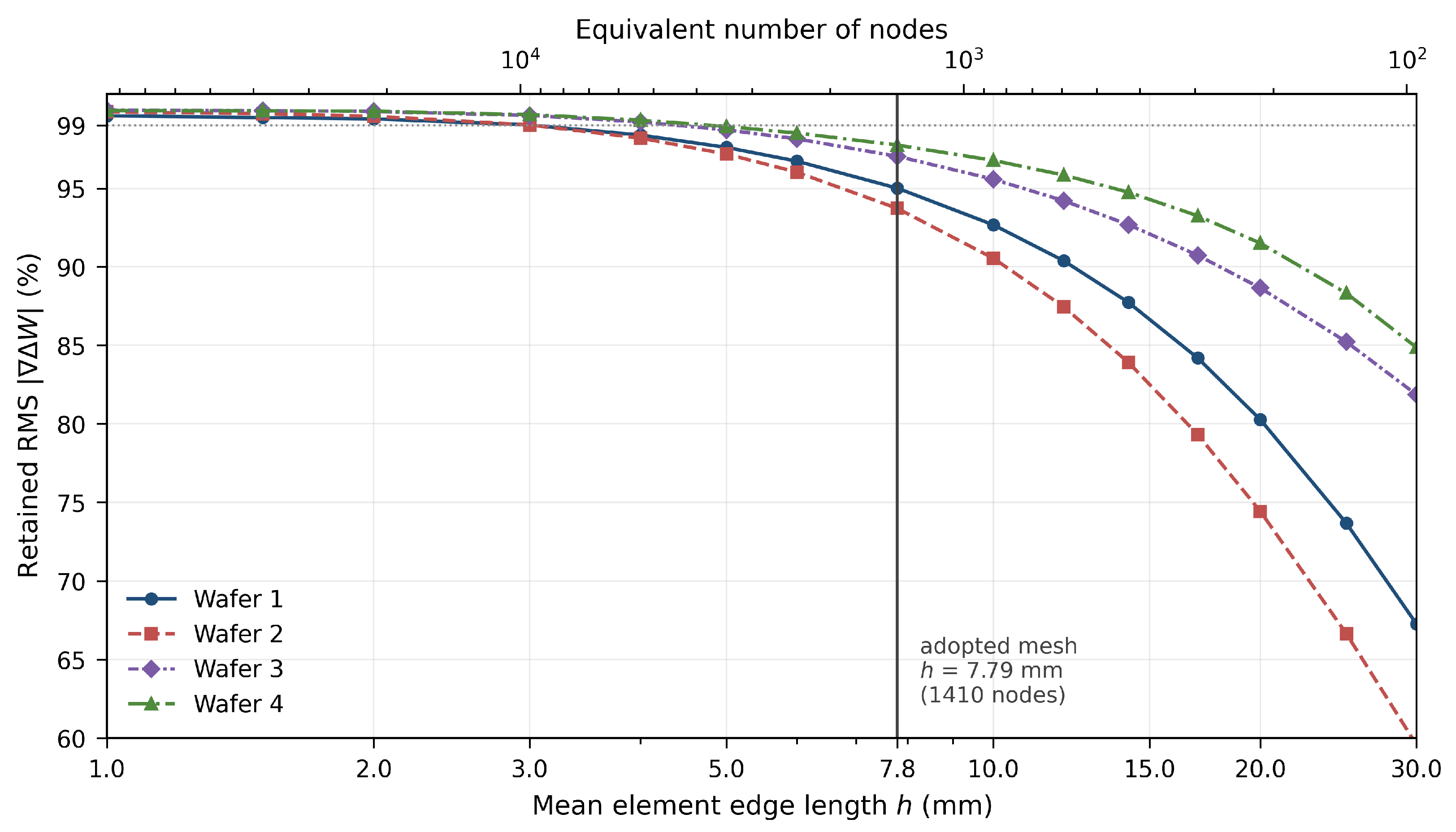
Rather than adopting these estimates a priori, the resolution actually required by each measurement can be determined directly from the data. The coupling operator involves derivatives of , so the quantity governing the necessary resolution is the spatial content of the surface gradient, not that of the height. Accordingly, each full-resolution map was progressively smoothed to the scale of the discretisation and the retained fraction of the RMS surface gradient, , was evaluated as a function of element size. A normalised convolution was used for the smoothing, so that no artificial slope is introduced at the aperture boundary; this is essential here, since the largest gradients, and hence the largest predicted displacements, occur precisely at the wafer edge.
Figure 6 shows the result. At the adopted element size the discretisation retains between 93.7% and 97.8% of the gradient content of the four measured maps, while a 99% target would require element sizes of 3.0–4.8 mm, that is between approximately 3600 and 9300 nodes.
Two features of
Figure 6 deserve comment. First, the required resolution is not governed by the deformation amplitude. Wafer 3 exhibits the largest gradient content of the dataset, 198 µrad RMS, yet is among the best resolved, because that gradient is distributed over long spatial wavelengths; Wafer 2, with 117 µrad, requires the finest discretisation of the four, since its gradient is concentrated in a localised edge feature. This mirrors the behaviour already observed for the predicted IPD in
Section 3.2 and has the same physical origin: the spatial distribution of the wafer geometry, rather than its overall amplitude, governs both the magnitude of the response and the resolution required to capture it.
Second, and of direct practical importance, the criterion is evaluated entirely from the measured map and requires no solution of the mechanical problem. The discretisation can therefore be selected before the analysis is run: for a given target retention level,
Figure 6 returns the element size required by that particular wafer, so that the resolution is matched to each measurement instead of being fixed a priori for the whole dataset. Combined with a precomputed library of factorised membrane operators, one per refinement level, this preserves the single-factorisation cost structure of the method while adapting the resolution to the data, and makes the spatial bandwidth of the prediction an explicitly reported property of each individual result.
3.3.3. Convergence Verification
A mesh convergence analysis was carried out prior to selecting the final discretisation [
52,
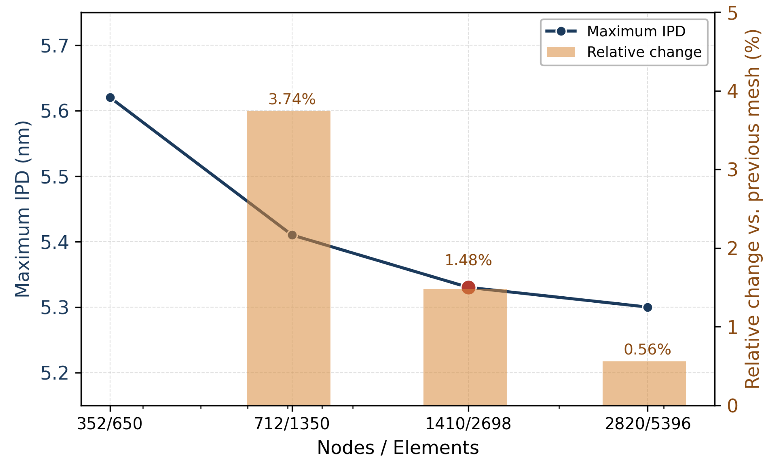
53]. Four progressively refined meshes were evaluated (352, 712, 1410 and 2820 nodes, with 650, 1350, 2698 and 5396 elements, respectively), monitoring the maximum IPD predicted. As shown in
Figure 7, the maximum IPD decreased monotonically from 5.62 nm (352 nodes) to 5.30 nm (2820 nodes), with the relative change between successive refinement levels dropping from 3.74% (352 → 712 nodes) to 1.48% (712 → 1410 nodes) and 0.56% (1410 → 2820 nodes), indicating that the solution had entered its asymptotic convergence range. The 1410-node, 2698-element mesh was therefore retained, as it lies within this converged range while maintaining a computational cost compatible with industrial applications.
The convergence behaviour of
Figure 7 is consistent with the gradient-retention criterion of
Section 3.3.2 and provides an independent a posteriori confirmation of the adopted discretisation: the refinement level at which the predicted IPD stabilises coincides with the level at which the gradient content of the measured maps is essentially fully resolved.
3.4. Role of Elastic Anisotropy
The constitutive model introduced in
Section 2.4 retains the cubic elastic anisotropy of monocrystalline silicon. This subsection quantifies what that choice contributes to the predicted IPD, by repeating the analysis of
Section 3.2 on identical wafer geometries and identical meshes, changing only the constitutive matrix.
The comparison requires a reference isotropic material, and its choice is not arbitrary: it must differ from the cubic matrix in the anisotropy alone, so that no other property is varied at the same time. This is achieved by the extensionally equivalent material, obtained by matching the extensional coefficients of Equation (
25) through
and
, which for silicon gives
GPa and
. The two constitutive matrices then share
and
and differ only in the shear coefficient,
GPa for the cubic material against
GPa for its isotropic counterpart, their ratio being the Zener factor of Equation (
19).
A single reference material is sufficient because the prediction is invariant to a uniform scaling of the constitutive matrix: appears as a common factor in both and and therefore cancels in the transfer operator. The result is governed by the shape of , that is by the shear-to-extensional ratio, and not by its magnitude, so an isotropic alternative adopting a different modulus, such as the value of 169 GPa often used for wafers, would not alter the comparison.
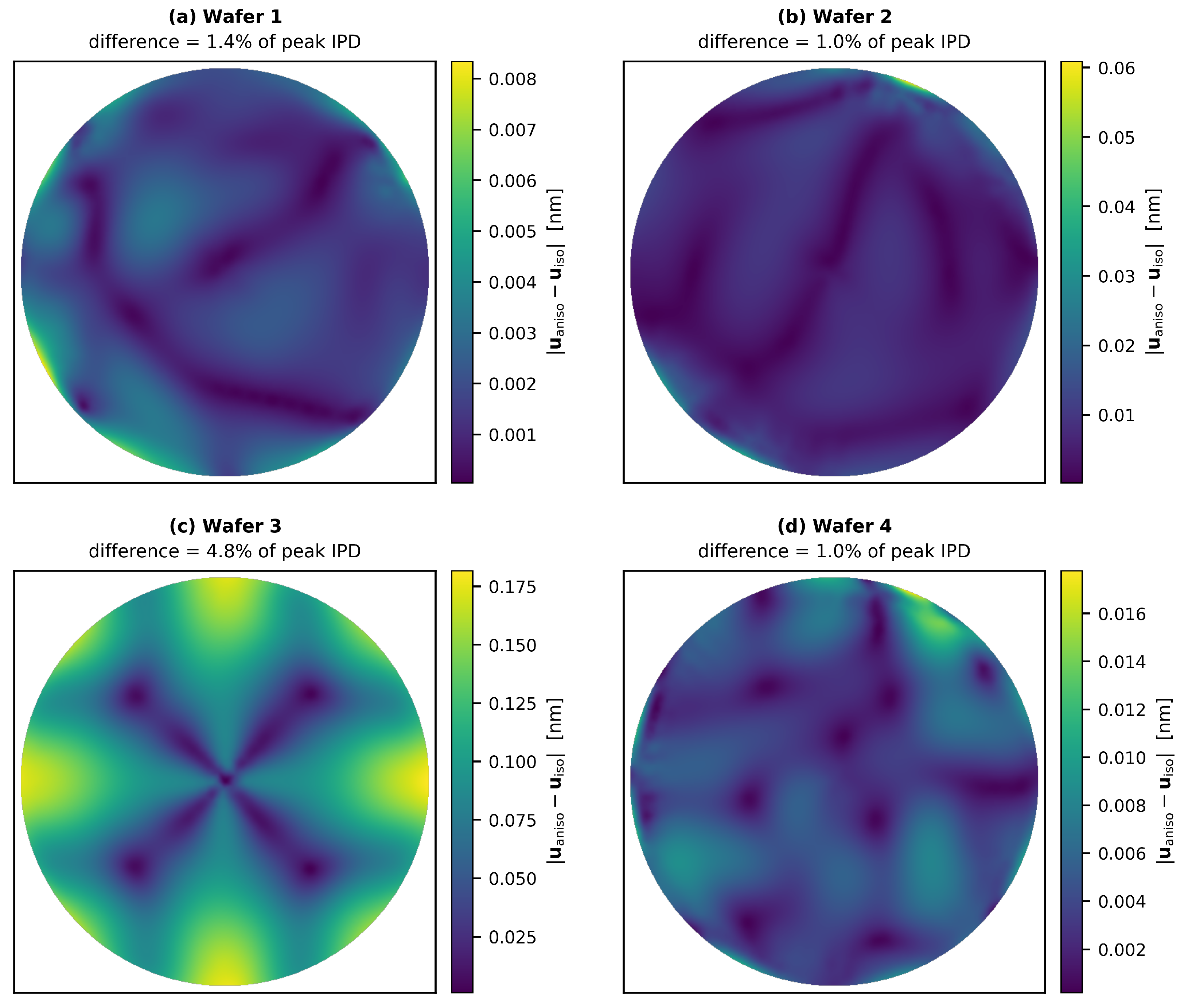
Figure 8 shows where the difference acts. For Wafer 3, whose geometry is the smoothest and most regular of the dataset, the difference field exhibits a clean four-fold angular pattern with its extrema on the
axes and its nodes on the diagonals. This is the symmetry of the
crystal plane, and it is not imposed anywhere in the formulation: it emerges from the constitutive matrix alone. In the remaining wafers the same signature is present but partially masked by the localised edge features that dominate their individual geometries. An isotropic model cannot generate an angular structure of this kind under any choice of constants, since an isotropic solid has no preferred material directions.
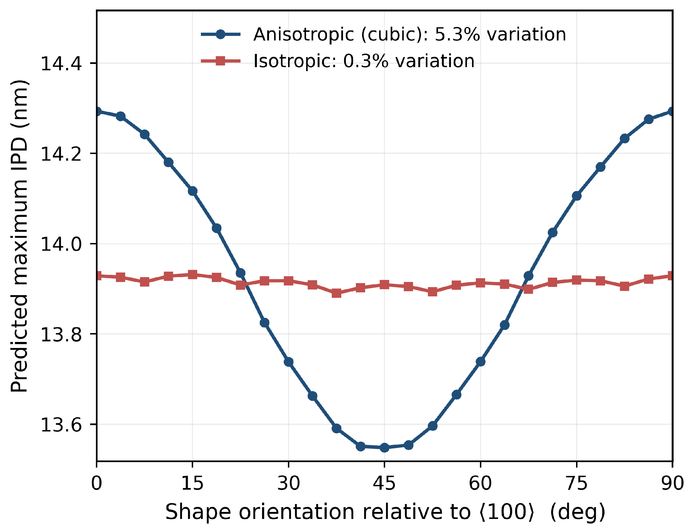
This observation admits a direct test that requires no reference isotropic material at all. A single shape, an astigmatic deformation of fixed PV amplitude, was rotated with respect to the crystal axes and the analysis repeated at each orientation. The geometry is identical in every case: same amplitude, same RMS, same spatial spectrum. Only its orientation relative to the lattice changes.
The outcome is shown in
Figure 9. The isotropic prediction varies by 0.3% across the full range, which is the discretisation noise of the mesh and is the expected result: an isotropic response cannot depend on orientation. The anisotropic prediction varies by 5.3%, with a minimum at 45°, maxima at 0° and 90°, and a period of 90° that reproduces the symmetry of the
plane. Because the isotropic model supplies its own null baseline, the entire departure from a flat response is attributable to the crystal anisotropy, with no dependence on the choice of reference elastic constants.
The practical consequence concerns the alignment convention. Two wafers carrying the same measured geometry but seated at different angular positions on the chuck are predicted to develop IPD differing by several per cent, and a model that ignores the crystal orientation cannot represent this difference.
3.5. Sensitivity to Metrology Noise
The prediction takes the measured wafer geometry as its only input, so the repeatability of the metrology propagates into the predicted distortion.
The path by which measurement noise reaches the mechanical model is determined by the transfer described in
Section 3. The measured map is not transferred to the mesh point by point: it is projected onto the Zernike basis of Equation (
51), truncated at radial order
and comprising
modes, and the resulting analytical surface is evaluated at each node of the finite-element mesh. Consequently, the reconstructed measurement uncertainty is restricted to the subspace spanned by those 66 retained modes. The dominant spectral filtering is therefore introduced by the Zernike projection before the reconstructed surface is evaluated at the mesh nodes. The mesh size does not define this spectral basis, although it may still affect the numerical representation of the reconstructed geometry and the resulting finite-element sensitivities.
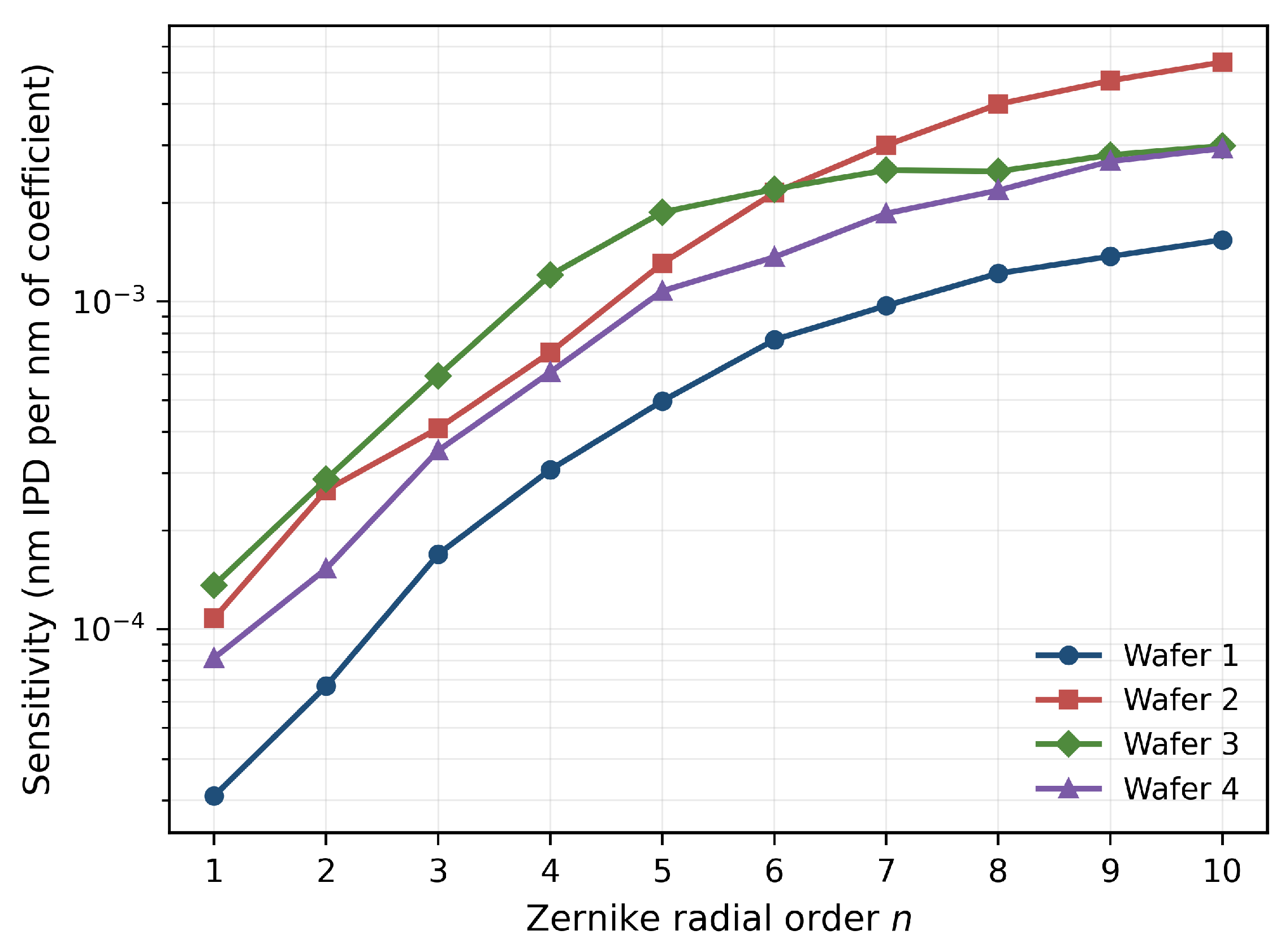
This structure allows the propagation of measurement uncertainty to be evaluated through a direct sensitivity analysis rather than by Monte Carlo sampling. Each Zernike mode was perturbed individually by a unit coefficient amplitude, and the mechanical problem was re-solved. The resulting change in the selected scalar metric of the predicted in-plane distortion defines the sensitivity coefficient , expressed in nanometres of IPD per nanometre of Zernike coefficient.
For a given distribution of the measurement uncertainty among the retained modes, the general linear uncertainty propagation can be written as
where
is the vector of modal sensitivity coefficients and
is the covariance matrix of the fitted Zernike coefficients. If the coefficient errors are assumed to be statistically uncorrelated,
The latter expression therefore assumes that the coefficient errors are uncorrelated and that the modal uncertainty budget is expressed using the same RMS convention as .
Figure 10 shows that the sensitivity is strongly dependent on the Zernike radial order, increasing by up to two orders of magnitude between the first and the tenth radial order. This trend is obtained from the present mechanical simulations and is not assumed a priori. For a fixed coefficient amplitude, higher-order modes generally exhibit shorter spatial scales and larger characteristic gradients, making them more influential in a gradient-driven distortion response.
The repeatability of the metrology platform used in this work has been characterised separately [
65]. For a blank 300 mm silicon wafer measured 30 times following SEMI M49, the reported RMS repeatability is 4.68 nm and 4.21 nm for the front and back sides under semi-static conditions, respectively. When manual loading and unloading of the wafer are included, these values increase to 20.19 nm and 29.10 nm, respectively. The value adopted here is
nm, chosen conservatively to cover the largest repeatability value reported in that study.
Since the spectral distribution and covariance of the measurement noise among the Zernike modes have not been characterised, the reported quantity is a conservative bound that does not require a specific modal noise distribution. For the linear sensitivity model, the bound is obtained by assigning the complete RMS uncertainty budget to the Zernike mode with the largest absolute sensitivity coefficient:
This represents the worst-case allocation of the available uncertainty power within the retained 66-dimensional Zernike subspace.
The resulting upper bounds for the four wafers are summarised in
Table 1.
The estimated metrology-induced uncertainty remains below 0.23 nm for all four wafers under the adopted uncertainty budget and linear sensitivity model. Because the calculation assigns the complete uncertainty budget to the most sensitive retained mode and uses the repeatability measured under manual wafer handling rather than the semi-static value applicable to the present measurements, the result provides a conservative estimate.
Under the assumptions of the present analysis, the contribution of metrology repeatability is therefore unlikely to be the dominant source of uncertainty in the predicted IPD. This conclusion remains conditional on the adopted Zernike truncation, the selected IPD metric, the assumed linear response, and the absence of a measured covariance structure for the fitted Zernike coefficients.
3.6. Computational Cost and Conditioning of the Condensed Operator
Both the cost of the method and its numerical accuracy are properties of the same object. The operator
depends only on the mesh, the material and the chucking configuration, not on the measured geometry: the wafer shape enters the system solely through the right-hand side
, where
is the prescribed out-of-plane state of Equation (
13) built from the measured field. Assembly, condensation and factorisation are therefore performed once for a given mesh and chuck, and each subsequent wafer requires only a matrix–vector product against the stored coupling block, followed by a single back-substitution against the stored factors.
The computational cost was measured on the workstation used in this study, equipped with an Intel Core i7-13700HX processor and 32 GB of RAM. The mesh contains 1410 nodes and 2698 triangular shell elements, which with six degrees of freedom per node gives 8460 degrees of freedom in total and a condensed membrane system of 4227 unknowns once the rigid-body modes are removed.
The separation between the two groups is the operative point. The set-up is paid once, in 1.19 s; thereafter the marginal cost of an additional wafer is 0.14 s, so that a batch of n wafers costs rather than n independent solutions.
The cost is also deterministic. The chucking condition is imposed as a prescribed displacement rather than resolved as a contact problem, so the system is linear and is solved in a single pass: there is no Newton loop, no convergence tolerance, and consequently no wafer that requires more iterations than another or that fails to converge at all. The figures in
Table 2 are therefore not averages but the cost of every wafer, which for an in-line application matters more than a lower mean, since the latency budget must be guaranteed rather than expected. For reference, the metrology platform used in this work acquires a full-aperture 300 mm wafer map in approximately 12 s [
65], so the prediction is completed well within the acquisition cycle of the measurement it consumes and does not constitute the throughput bottleneck of a combined measure-and-predict operation.
The in-plane displacements associated with
are small enough that the changes they induce in
are negligible for the wafer shapes considered here, so a single evaluation of its conditioning is representative of the whole dataset. The spectral condition number, obtained from the singular value decomposition of the condensed operator [
61], is
which, from Equations (
49) and (
50), corresponds to
lost decimal digits and
effective significant digits under IEEE double-precision arithmetic. With the model geometry expressed in centimetres over a wafer radius of 15 cm, this leaves an absolute numerical resolution of the order of
nm, several orders of magnitude below the nanometre-scale distortions of interest.
The error introduced by the solution procedure is therefore negligible relative to the quantity being predicted, and reusing a single factorisation across the dataset does not degrade it. Taken together with the uncertainty bound of
Section 3.5, neither the numerical solution nor the repeatability of the metrology limits the prediction at the present level of accuracy; the limiting factor is the set of modelling assumptions discussed in
Section 2.3.
4. Conclusions
This work has presented a transparent finite-element framework for predicting chucking-induced IPD directly from measured wafer out-of-plane geometry. The proposed methodology combines the ANDES shell formulation [
34,
35] with a static-condensation strategy [
39] that transforms the measured OPD field into the corresponding IPD without requiring any knowledge of the underlying stress distribution responsible for the wafer deformation.
The finite-element formulation accounts for the two-dimensional mechanics of wafer flattening, arbitrary non-axisymmetric geometries, and the anisotropic elastic behaviour of monocrystalline silicon [
45]. The explicit partitioning of the global stiffness matrix leads to a direct OPD-to-IPD transfer operator, allowing the chucking-induced in-plane response to be computed from measured wafer geometries. The operator can be efficiently reused for different wafer measurements when the mesh, material properties, and chuck configuration remain unchanged.
Application of the methodology to four representative industrial wafer measurements demonstrates that the predicted IPD strongly depends on the spatial distribution of the wafer geometry rather than solely on its overall amplitude. Wafers exhibiting similar peak-to-valley values may therefore produce substantially different in-plane distortion fields, highlighting the limitations of global shape metrics as predictors of overlay performance [
29].
The numerical formulation also exhibits favourable computational properties. Assembly, condensation and factorisation take 1.19 s for the mesh used here, after which each additional wafer costs 0.14 s, so that computational costs remain compatible with high-throughput, metrology-driven feed-forward applications [
21,
28]. The condensed membrane system remains well conditioned, with
corresponding to an absolute numerical resolution of the order of
nm, which provides sufficient numerical precision for nanometre-scale displacement prediction. The uncertainty propagated from the repeatability of the metrology remains below 0.23 nm, so that neither the numerical solution nor the measurement is the factor limiting the prediction.
The natural next step of this work is the experimental validation of the predicted displacement fields. Such validation requires direct measurement of wafer-scale in-plane displacements with nanometre accuracy after chucking, which currently demands highly specialised overlay metrology equipment or dedicated lithographic measurement platforms [
66] that are generally available only in advanced semiconductor manufacturing facilities. Experimental confirmation of the proposed model under controlled chucking conditions will therefore constitute the subject of future work and will enable a quantitative assessment of the predictive capability of the proposed framework.





 ,
,