

Article

Design and Computational Potential of Circuit-Based Multiple-Electron Network Model

1
Graduate School of Engineering Science, Yokohama National University, Yokohama 240-8501, Japan
2
Semiconductor and Quantum Integrated Electronics Research Center, Institute for Multidisciplinary Sciences, Yokohama National University, Yokohama 240-8501, Japan
*
Author to whom correspondence should be addressed.
Appl. Sci. 2026, 16(17), 8506; https://doi.org/10.3390/app16178506
Submission received: 15 July 2026 / Revised: 17 August 2026 / Accepted: 23 August 2026 / Published: 26 August 2026
(This article belongs to the Section Applied Physics General)

Abstract

Complex nonlinear physical systems can exhibit dynamic responses that provide useful resources for information processing. In this study, an electrical circuit-based multiple-electron model was developed and implemented in a random network to investigate its dynamic electrical properties and information-processing capability. The model represents discrete electron transfer and charge accumulation using tunnel junctions and charge-storage nodes and was constructed as a two-dimensional random network inspired by carbon nanotube/polyoxometalate (CNT/POM) networks. The network exhibited time-varying current responses under a constant voltage and nonlinear and hysteretic current–voltage characteristics. The hysteresis became more pronounced as the number of charge-storage nodes increased. The information-processing capability of the network was further investigated using delayed XOR and sine waveform generation tasks. The delayed XOR task was achieved using the integrated squared current response, whereas a target sine waveform was reconstructed from multiple network responses under a constant voltage input using a linear readout, yielding a coefficient of determination of 0.816. These results demonstrate that the proposed multiple-electron network exhibits nonlinear and history-dependent electrical dynamics and can support information-processing tasks.

1. Introduction

Complex nonlinear physical systems exhibit characteristic dynamics governed by their underlying physical mechanisms. The dynamics produced by such systems can be exploited as resources for information processing [1,2,3]. Reservoir computing is a promising framework for utilizing these dynamics [4,5,6]. It has been implemented using a wide variety of physical systems [7,8,9].
Some complex physical systems consist of many elements connected in a network. The individual elements can exhibit their own characteristic behaviors and interact with one another through the network, giving rise to complex dynamics at the system level [10].
Nanomaterials provide a means of forming such networked physical systems. Conductive nanomaterials can naturally form network structures into which components such as molecules with their own characteristic behaviors can be incorporated. Combining these components allows the local behavior of individual elements to influence other parts of the system through the conductive network. Complex system-level dynamics can accommodate structural randomness, while the resulting heterogeneity in network structure can influence the dynamics of the overall system. Randomly formed nanomaterial networks therefore provide a natural platform for constructing such complex physical systems [11,12].
A carbon nanotube/polyoxometalate (CNT/POM) random network is one example of such a material system. CNTs form conductive pathways [13], while POMs are redox-active molecular clusters capable of storing multiple electrons [14,15]. Spike-like currents and nonlinear electrical characteristics have been experimentally observed in CNT/POM random networks [16].
Previous studies have modeled CNT/POM random networks using cellular automaton (CA) models composed of interconnected cells, in which discrete charge accumulation and release are described by phenomenological, threshold-based transition rules [16]. Analog CA models have also been proposed as circuit-based networks of nodes interconnected by nonlinear resistors [17].
In a CNT/POM network, POMs can be regarded as charge-storage nodes, while the regions through which electrons are transferred between conductive CNT pathways and POMs can be represented as junction-like structures. Based on this correspondence, a single-electron circuit model consisting of tunnel junctions and charge-storage nodes was first considered [18,19,20]. To account for the accumulation and release of multiple electrons in POMs, the model was then extended to a multiple-electron model [21,22].
The resulting framework is circuit-based, as are the analog CA models described above, while also incorporating discrete charge accumulation and release, as in the phenomenological CA models.
In this study, the proposed multiple-electron model was implemented in a two-dimensional random network inspired by CNT/POM networks. Its dynamic electrical properties were investigated through temporal current responses and current–voltage (I–V) characteristics. The information-processing capability of the network was further investigated using delayed XOR and sine waveform generation tasks.

2. Multiple-Electron Model

2.1. Concept of Multiple-Electron Model

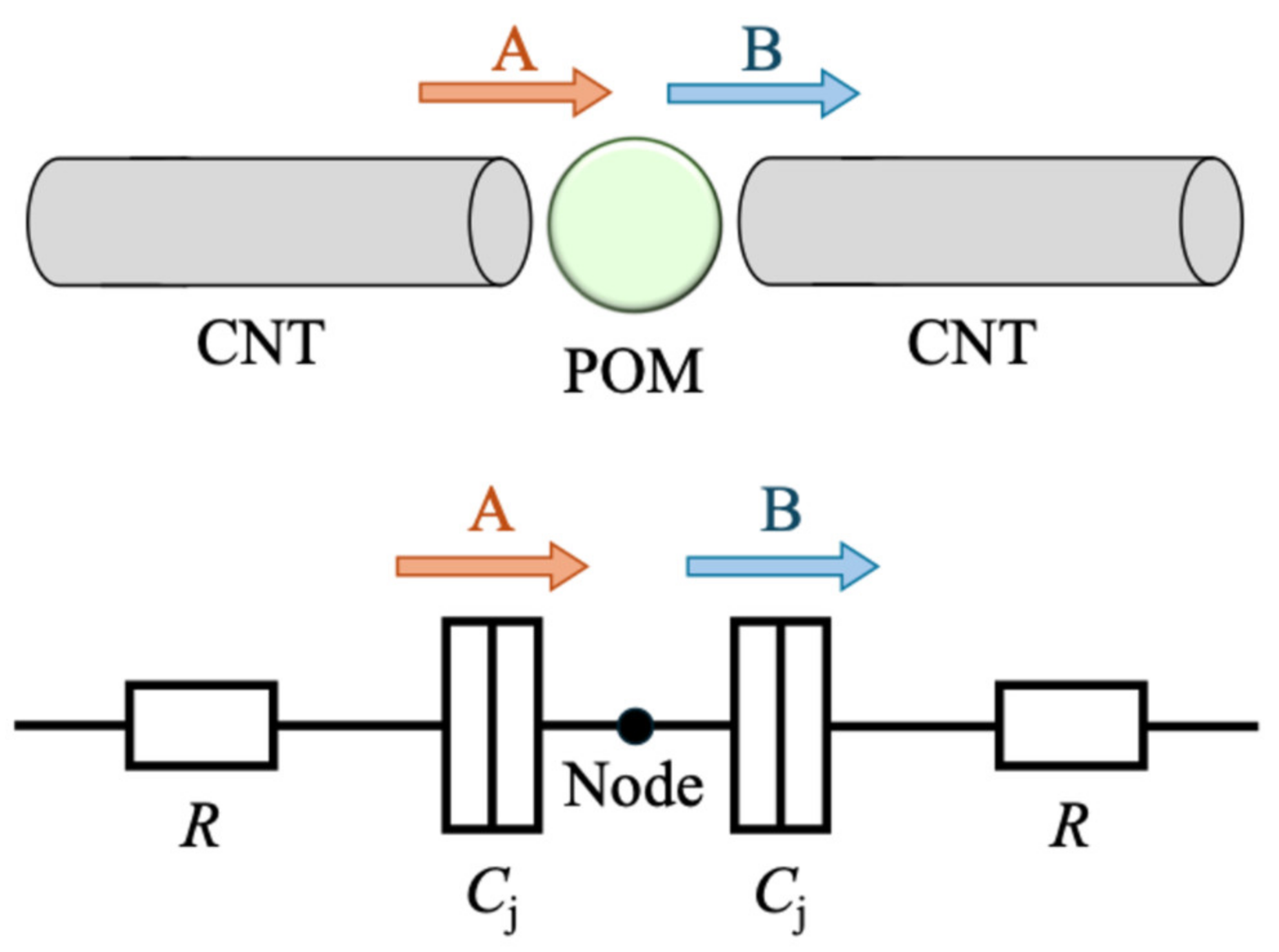
Figure 1 illustrates the conceptual correspondence between the physical structure of a CNT/POM network and the proposed circuit model. In this representation, CNTs are modeled as conductive wires (resistors), the CNT–POM interfaces are represented by tunnel junctions, and the POM molecule is regarded as a charge-storage node. This abstraction provides a circuit-based framework for investigating nonlinear charge-transport systems.
Unlike conventional single-electron circuits, the proposed model assumes that charge-storage nodes can accumulate multiple electrons before releasing them. This extension enables the model to represent collective charge-storage and release processes that are expected to occur in redox-active materials.

2.2. Circuit Representation and Electron-Transfer Mechanism

The basic unit of the proposed model consists of a resistor–junction–node–junction–resistor structure, as shown in Figure 1. Electron transport through the tunnel junctions is simulated using a Monte Carlo method based on the Coulomb blockade condition. In the conventional single-electron model, an electron transition is allowed when the electrostatic energy of the system decreases, namely,
E = E b e f o r e E a f t e r > 0 .
In the proposed model, inward electron transport from a resistor to a charge-storage node is allowed when E   >   0 , following the transition rule of the conventional single-electron model.
In contrast, outward electron transport is additionally constrained by charge accumulation. An electron is allowed to tunnel from a charge-storage node to a neighboring resistor only when both Δ E > 0 and Q > Q t h are satisfied, where Q denotes the number of accumulated electrons and Q t h is the threshold charge.
To represent the possible influence of charge accumulation on the surrounding conductive paths, which may arise from changes in the local electronic state around redox-active materials, a phenomenological charge-dependent resistance was introduced:
R = R 0 exp ( β Q ) ,
where R 0 is the baseline resistance, Q is stored charge, and β is a phenomenological parameter that controls the degree of resistance modulation.
Unless otherwise specified, Q t h = 20 and β = 0.2 were used as the reference values. The physical interpretation of these parameters is discussed in Section 5, while their influence on the network response is examined through the parameter scans described in Section 3.

2.3. Construction of Multiple-Electron Random Network

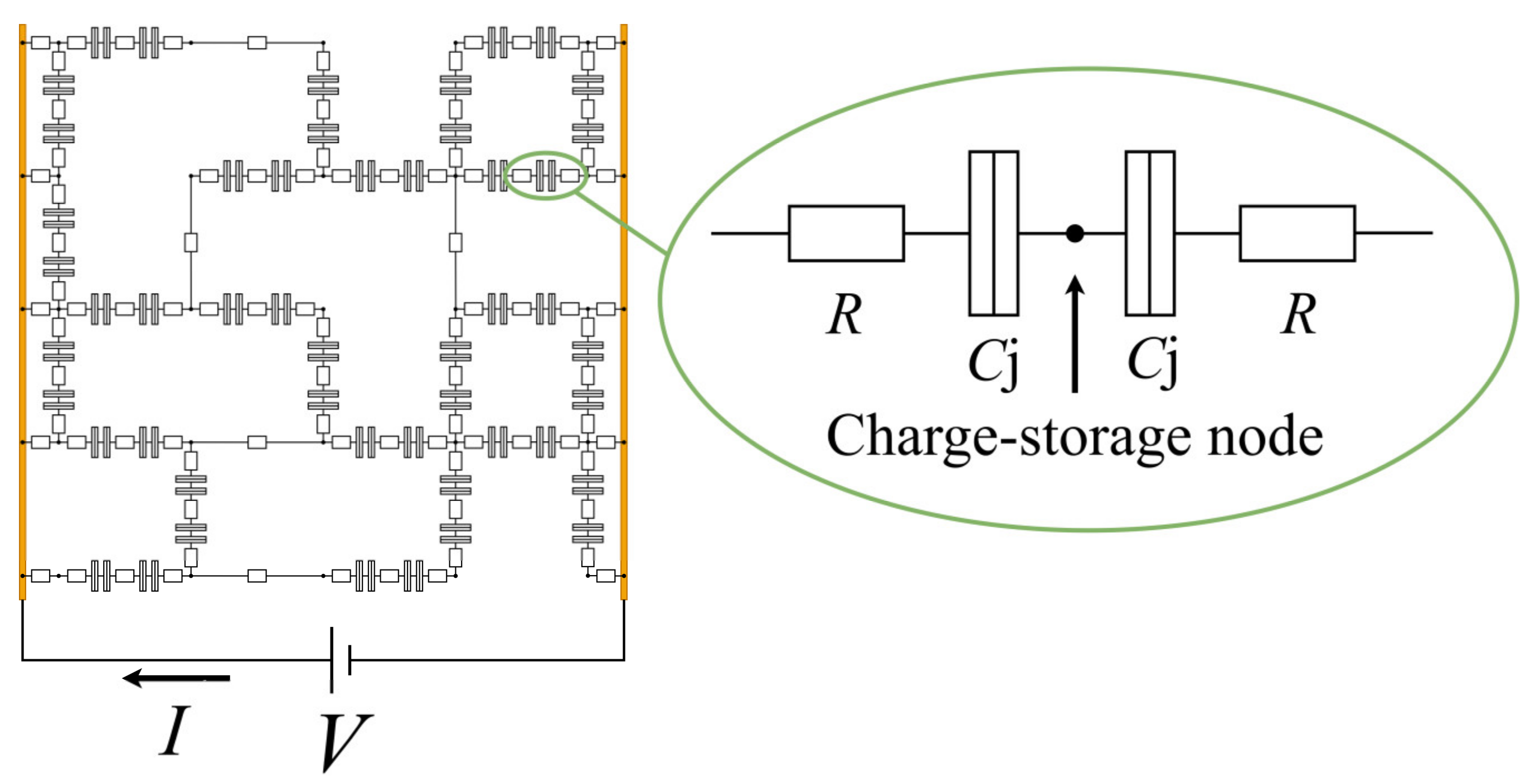
The multiple-electron units are arranged into a two-dimensional random network (Figure 2). The network is placed between two electrodes across which an external voltage is applied. The network is represented as a square-grid circuit consisting of 25 electrical nodes arranged in five rows and five columns. The five electrical nodes along each of the left and right edges are connected to the corresponding electrode through simple resistors. Of the 40 candidate internal edges, 10 were removed to introduce structural irregularity, corresponding to an edge-removal rate of 25%, leaving 30 internal edges. Each retained internal edge is configured either as a resistor edge or as a multiple-electron edge. Resistor edges provide purely resistive connections. Each multiple-electron edge contains two multiple-electron units; consequently, two charge-storage nodes are embedded along each multiple-electron edge. These charge-storage nodes are distinct from the electrical nodes that form the circuit connections. Unless otherwise specified, the reference network contains 50 charge-storage nodes distributed across 25 multiple-electron edges.
The resistance and junction-capacitance values were assigned from predefined distributions to introduce component-level variability. Unless otherwise specified, the simulations were performed using the same reference network configuration. Within each parameter scan, the network configuration and all parameters other than the parameter under investigation were held fixed. Each condition was evaluated in a single simulation run. The simulation time step was set to 0.05 ns, and all charge-storage nodes were initialized with zero charge. Definitions and numerical values of the circuit parameters are summarized in Appendix A.
In this network, electron release from one charge-storage node can promote charge accumulation at neighboring nodes. Consequently, electron-transfer events can propagate through the network as a cascade.

3. Dynamic Properties

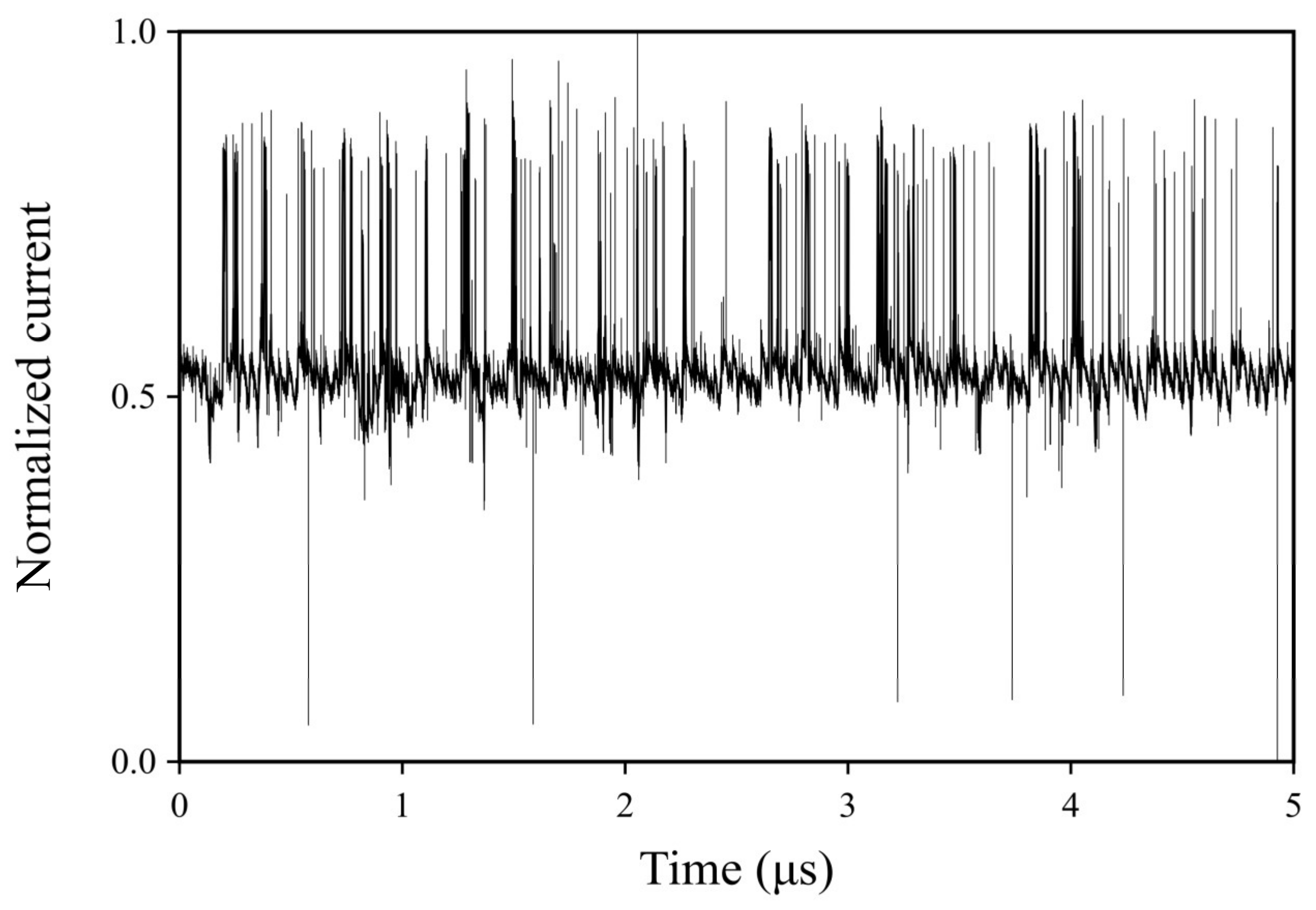
A constant voltage was first applied to the multiple-electron random network, and the temporal response of the current flowing through the network was monitored in the simulation. The voltage was swept from 0 to 40 V at 108 V/s and then held at 40 V for 50 μs. Figure 3 shows the fluctuating current response measured from 40 to 45 μs after the voltage reached 40 V.
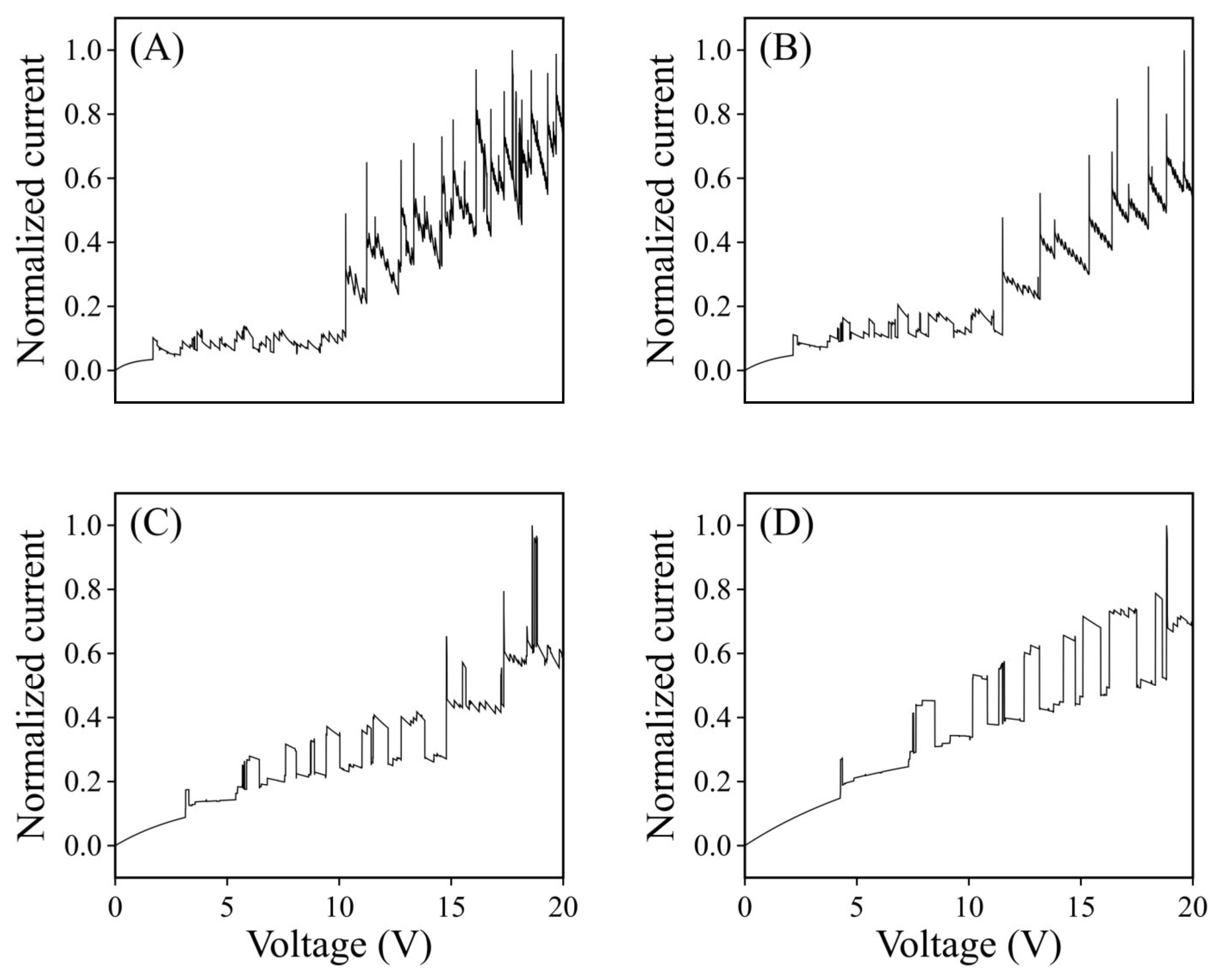
To further investigate the dynamic properties of the network, I–V measurements were simulated. Because the current response varies over time even under a constant voltage, the voltage sweep rate can affect the observed I–V characteristics. Accordingly, the applied voltage was swept at four different rates: 107, 2 × 10⁷, 5 × 10⁷, and 108 V/s. Figure 4 shows the resulting I–V characteristics. At the slowest sweep rate (Figure 4A), pronounced collective pulse-like responses emerged, particularly in the higher-voltage region. At higher sweep rates, these collective responses became less prominent, and more discrete step-like changes were observed.
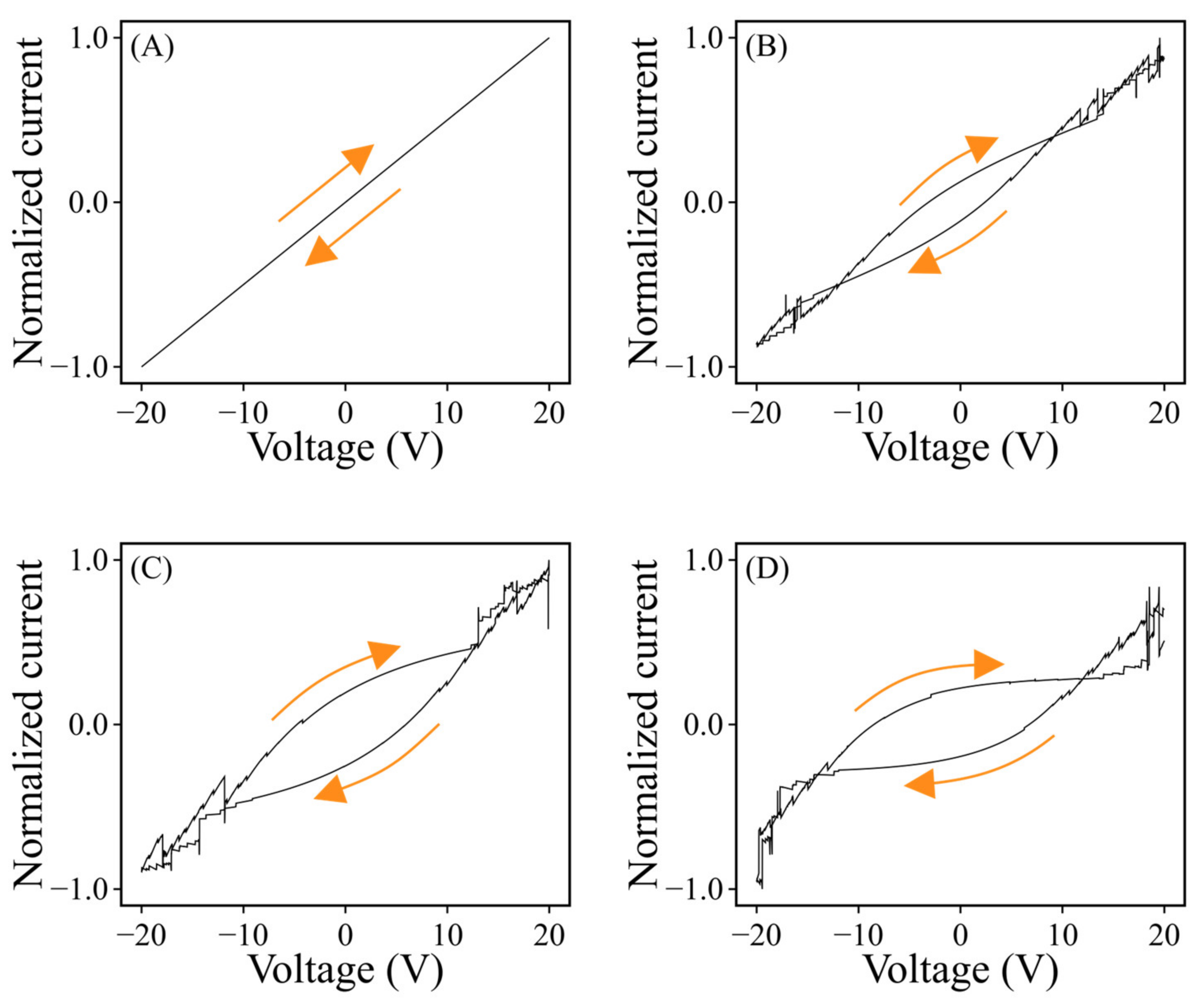
The applied voltage was swept from 0 V to +20 V, then to −20 V, and finally back to +20 V at a constant sweep rate of 108 V/s. To investigate the influence of charge-storage nodes on the resulting I–V characteristics, their number in the network was set to 0, 10, 30, and 50. The resulting I–V characteristics are shown in Figure 5. The initial sweep from 0 to +20 V is omitted, and only the subsequent sweep segments are shown. When the number of charge-storage nodes was small, the I–V characteristics showed only slight hysteresis. As the number of charge-storage nodes increased, the hysteresis became more pronounced, with the loop size expanding accordingly. These results indicate that increasing the number of charge-storage nodes enhances the hysteretic behavior of the network.
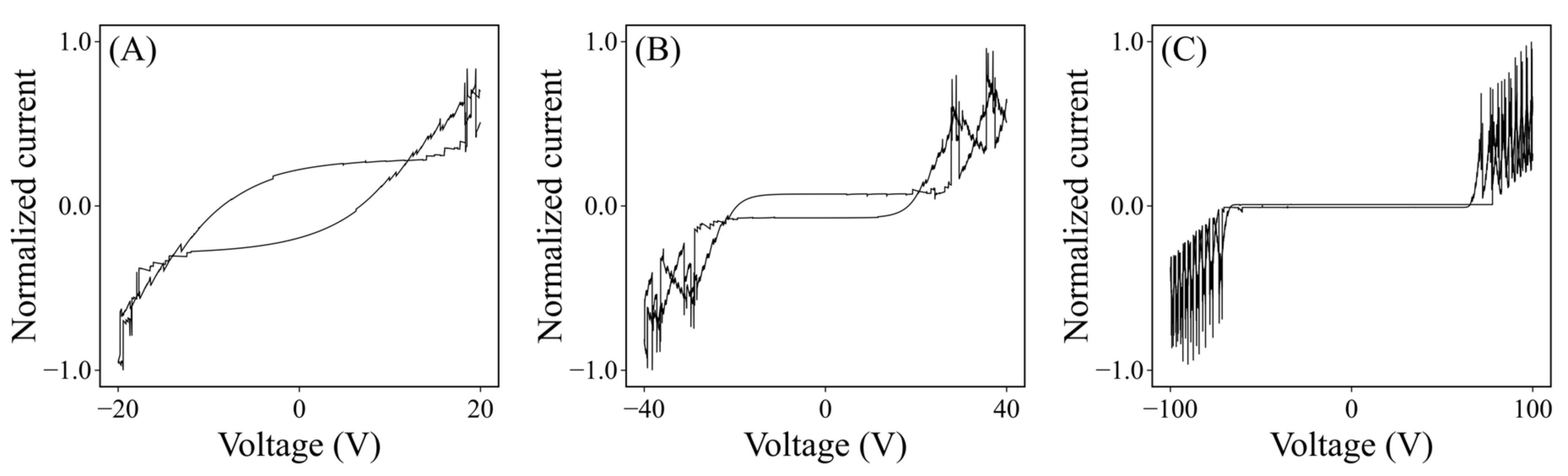
The junction capacitance was varied to investigate its effect on the I–V characteristics. The network configuration and other circuit parameters were kept unchanged. The number of charge-storage nodes was fixed at 50, and the voltage was swept under the same conditions as those used for Figure 5. The resulting I–V characteristics for C j / C * = 0.7, 0.3, and 0.1 are shown in Figure 6. As the junction capacitance decreased, the I–V characteristics changed from a pronounced hysteretic response to a response exhibiting clearer current onsets on both the positive- and negative-voltage sides. The current onsets also shifted toward higher absolute voltages. At C j / C * = 0.1, the positive-voltage current onset was observed at approximately 78 V.
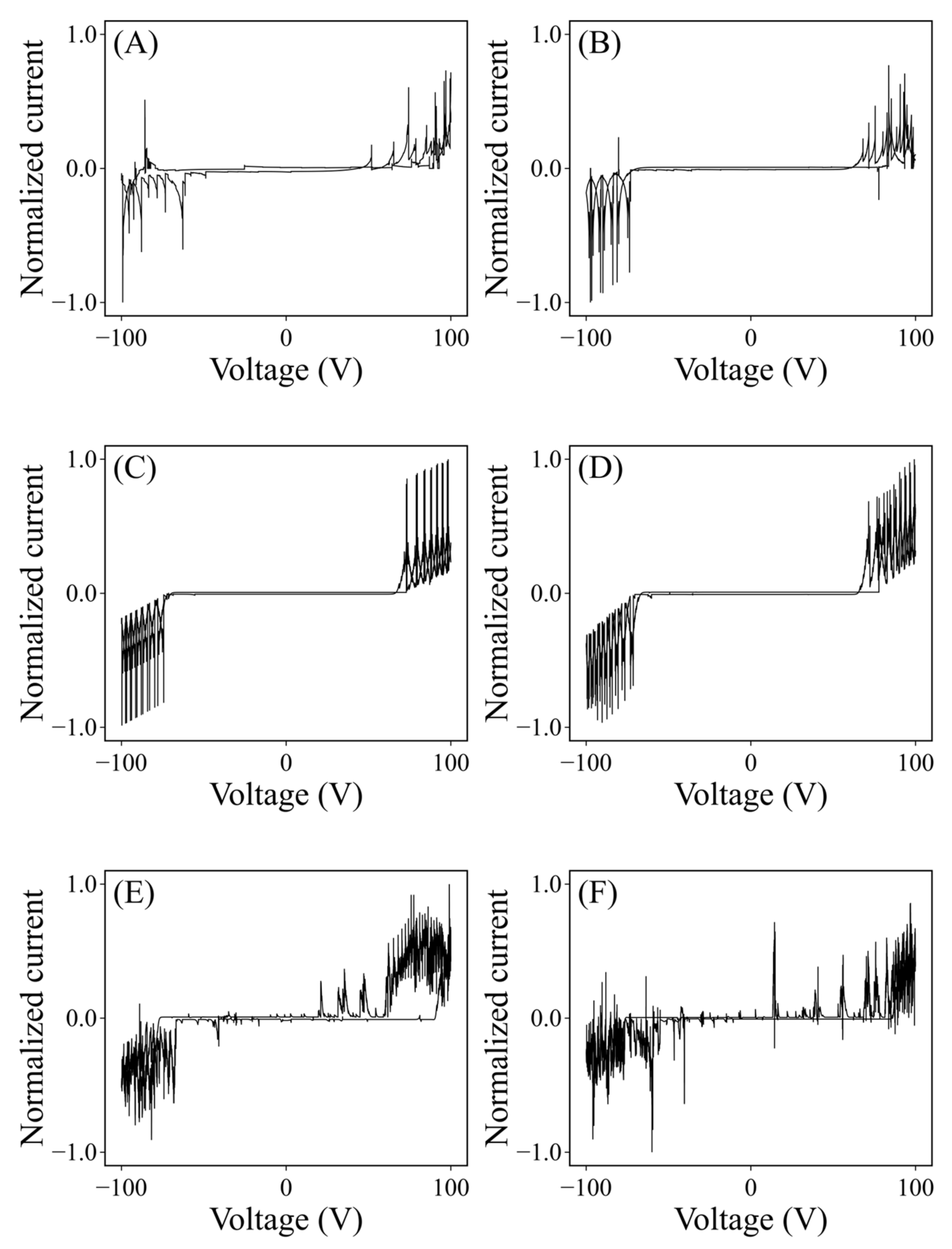
Based on the capacitance dependence observed in Figure 6, C j / C * = 0.1 was adopted as the reference capacitance for the subsequent β and Q t h parameter scans. The scans were performed from the Figure 6C condition, with Q t h = 20 for the β scan and β = 0.2 for the Q t h scan, while the network configuration and all remaining circuit parameters were held fixed. As shown in Figure 7, irregular pulse-like responses emerged in the otherwise nearly flat low-absolute-voltage region as β increased. As shown in Figure 8, the current onset shifted toward higher absolute voltages with increasing Q t h .

4. Information-Processing Capability

The information-processing capability of the multiple-electron random network was investigated using two tasks. For both tasks, the reference network containing 50 charge-storage nodes with C j / C * = 0.7 was used. A delayed XOR task was used to investigate memory and nonlinear information-processing capabilities [23], while sine waveform generation was used to examine the capability of the network to reconstruct a temporal waveform [24].

4.1. Delayed XOR Task

A randomly generated binary input sequence u ( n ) , consisting of 0 and 1, was used as the network input. The target output was defined as the exclusive OR (XOR) of the current input bit and the previous input bit:
t ( n ) = u ( n ) u ( n 1 ) .
The delayed XOR task is not linearly separable and depends on both the current and previous inputs. Therefore, successful classification requires both nonlinear information processing and information about the input history.
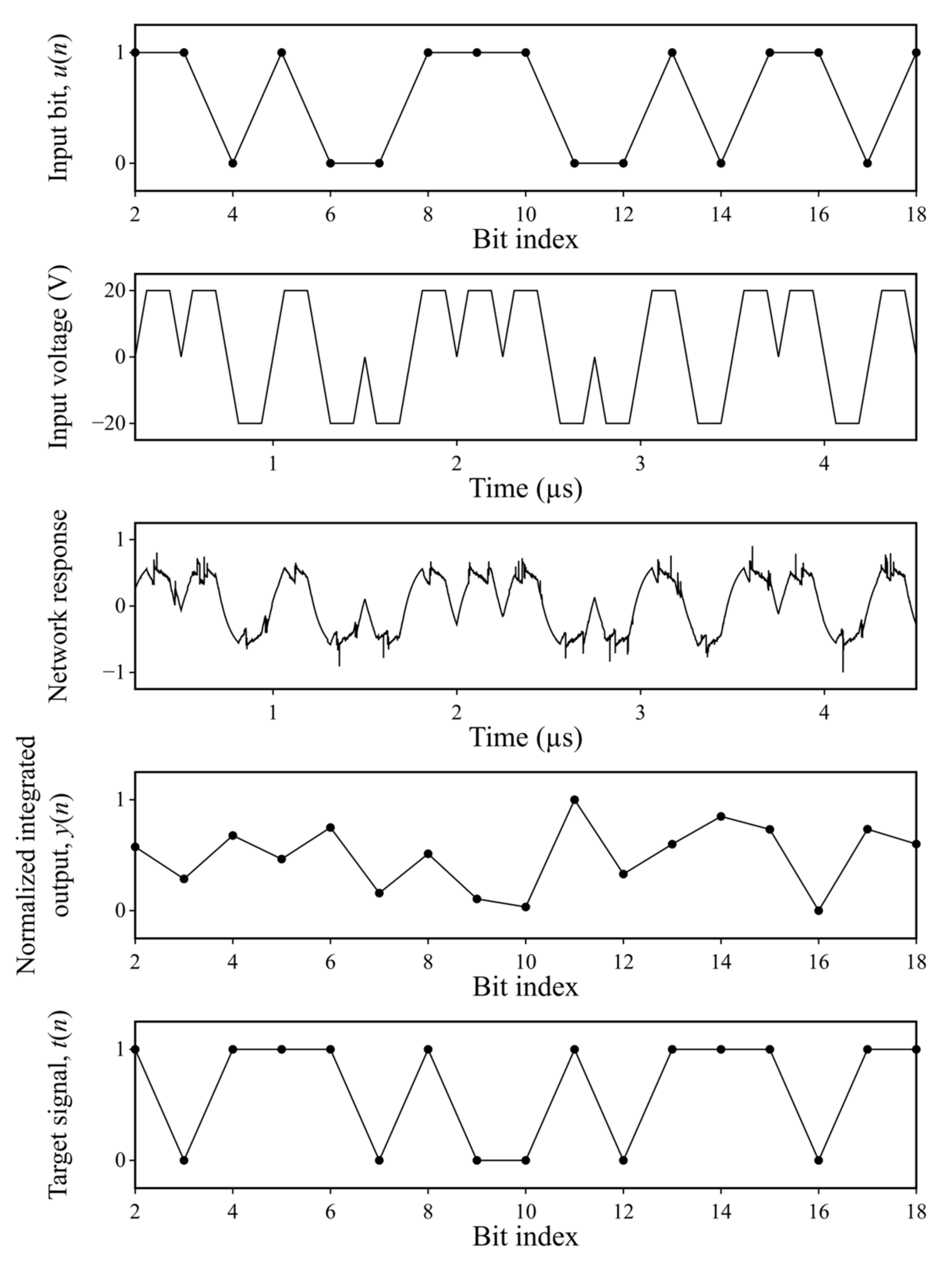
The binary sequence u ( n ) was converted into a trapezoidal input-voltage waveform, where binary values of 0 and 1 corresponded to −20 V and +20 V, respectively. Each bit interval corresponded to 0.25 μs. The first input interval was excluded from the analysis to avoid the initial transient and because no preceding bit was available for defining the delayed-XOR target.
The current response was monitored throughout the simulation. For each input interval, the squared current values were summed over the corresponding time window, and the resulting integrated values were normalized using min–max normalization as
y ~ ( n ) = t I ( t ) 2 ,
y ( n ) = y ~ ( n ) min y ~ ( n ) max y ~ ( n ) min y ~ ( n ) ,
where I ( t ) is the current at time step t , y ~ ( n ) is the integrated squared current for the n-th input interval, and y ( n ) is its min–max-normalized value.
Figure 9 shows the binary input sequence, the corresponding input voltage waveform, the network response, the normalized integrated output, and the target XOR signal.
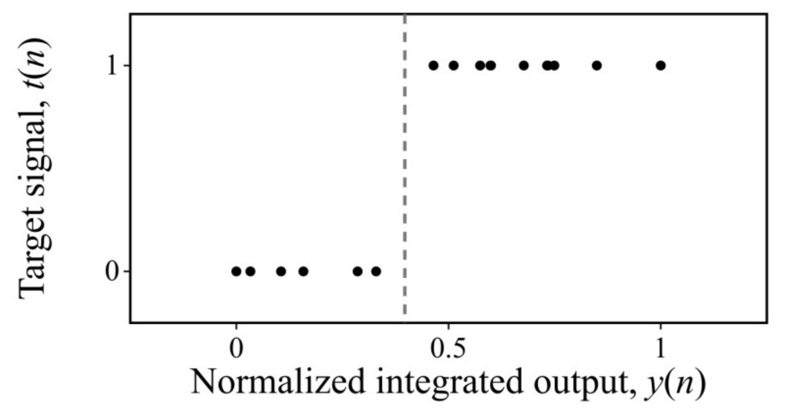
Figure 10 plots the normalized integrated output y ( n ) against the target signal t ( n ) . The output values corresponding to t ( n ) = 0 and t ( n ) = 1 are clearly separated. The dashed line represents the threshold defined as the midpoint between the maximum y ( n ) for t ( n ) = 0 and the minimum y ( n ) for t ( n ) = 1 , illustrating that a single threshold is sufficient to distinguish the two classes.

4.2. Sine Waveform Generation

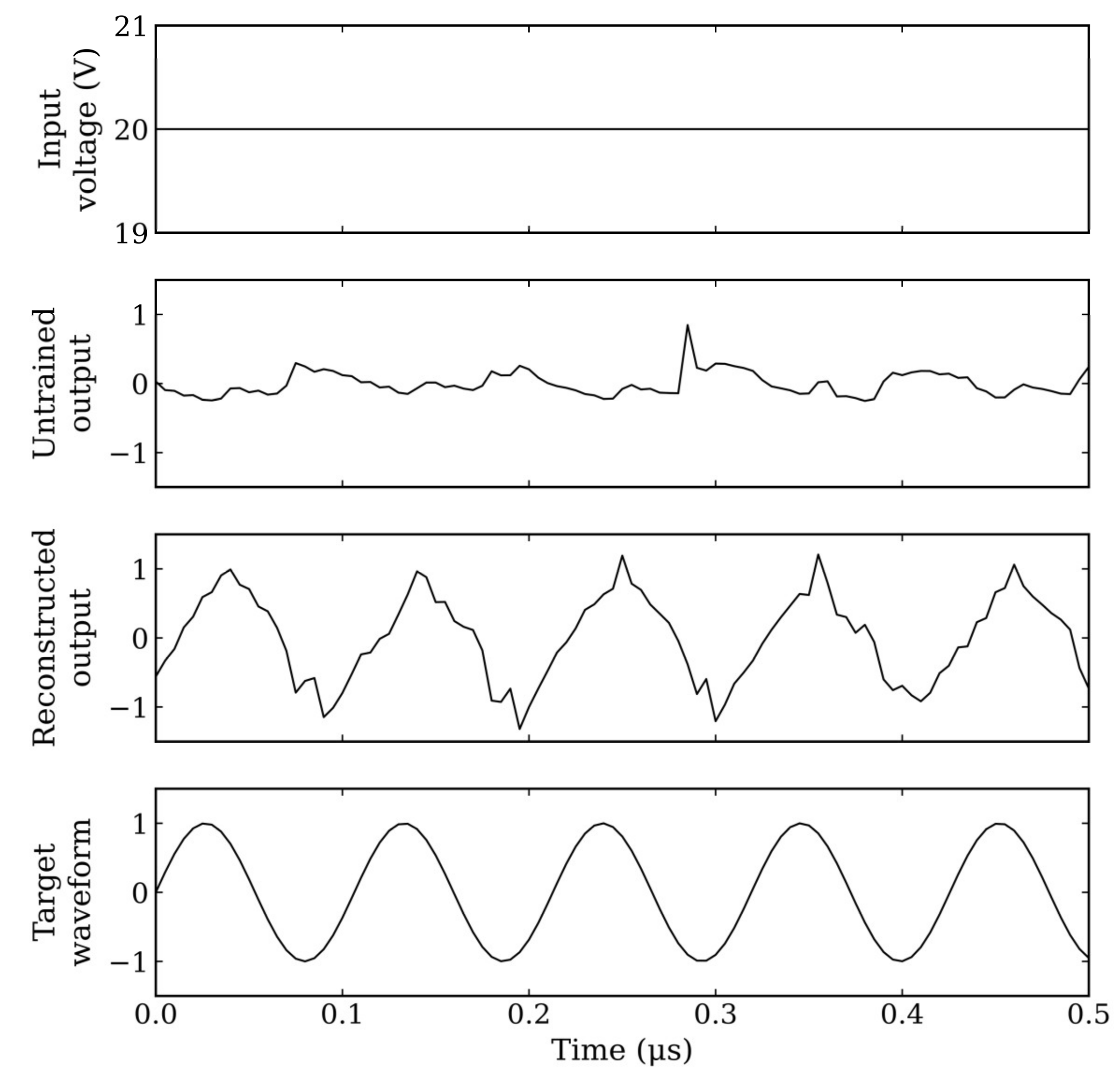
A constant voltage of 20 V was applied to the network, and current responses were obtained from 20 observation points. After the voltage reached 20 V, the first 10 μs of the constant-voltage response were excluded. The observation currents were then averaged over 5 ns intervals and used as the network states. Each response signal was standardized using z-score normalization. The readout weights were determined by linear Ridge regression to reconstruct the target sine waveform. The reconstruction performance was evaluated using the mean square error (MSE) and the coefficient of determination ( R 2 ).
Figure 11 shows the input voltage, the untrained output, the reconstructed output, and the target sine waveform. The untrained output was obtained using uniform readout weights before Ridge regression. The target frequency was approximately 9.40 MHz, corresponding to a period of approximately 106 ns. After Ridge regression, the reconstructed waveform closely followed the target waveform, yielding an MSE of 0.0922 and an R 2 score of 0.816. The dependence of sine waveform reconstruction performance on the network configuration is examined in Appendix C.

5. Discussion

The sweep-rate dependence can be understood in terms of the competition between the timescale of the voltage sweep and that of the propagation of cascading electron release. At slow sweep rates, sufficient time is available for cascades to develop, resulting in sharp pulse-like features in the I–V characteristics. At faster sweep rates, the collective pulse-like responses became less prominent, and more discrete step-like changes were observed. Since electron transport becomes faster at higher applied voltages, cascade propagation also accelerates. Consequently, even at the highest sweep rate, the current response becomes increasingly fluctuating in the high-voltage region.
In the present model, hysteresis arises from history-dependent charge accumulation in the network. Introducing more charge-storage nodes enhances the influence of the charge state on the current response. Consequently, the hysteresis becomes more pronounced as the number of charge-storage nodes increases.
The junction capacitance was found to be one of the factors governing the voltage scale of the simulated I–V characteristics. Decreasing C j made the current onsets at positive and negative voltages more apparent and shifted them toward higher absolute voltages. At C j / C * = 0.1 , the positive-voltage onset was approximately 78 V, approaching the experimental voltage scale near 80 V reported for the CNT/POM network [16]. However, agreement in the onset voltage alone does not establish quantitative correspondence with the experimental device. The simulated voltage response may also depend on the resistance parameters, network structure, and the values of β and Q t h governing charge-dependent resistance and electron release, respectively.
POMs are redox-active molecular oxides capable of accepting multiple electrons, and their electronic properties depend on their oxidation state and surrounding chemical environment. Electrochemical single-molecule measurements have resolved distinct conductance states associated with different oxidation states of a POM molecule [25]. In addition, the conductivity of POM molecular junctions has been reported to vary with the counter cation [26]. These observations provide an experimental basis for representing the influence of the stored-electron state on the effective resistance of the surrounding conductive path.
One possible microscopic interpretation of this charge-dependent resistance is a change in the electronic structure of the POM upon successive reduction. Successive reduction changes the charge state and electronic structure of the POM, including the energies and occupations of the electronic levels relevant to charge transport. These changes may alter the alignment between the transport-relevant electronic levels of the POM and those of the CNT, thereby modifying the effective resistance.
The available molecular studies do not provide a transferable numerical relation between the addition of one electron and the corresponding resistance change in a CNT/POM network. Accordingly, β is treated as an effective parameter describing the sensitivity of the effective resistance to accumulated charge, rather than as a direct representation of the changes in electronic levels or states associated with charge accumulation. β is not regarded as a universal value and may vary with the POM species, oxidation state, counter cation, electrode coupling, and solvent or hydration environment. Because the electronic-level alignment at the CNT/POM interface was not directly evaluated in this study, this mechanism remains one possible physical origin of the modeled resistance modulation.
The influence of β on the simulated network response was examined using the parameter scan shown in Figure 7. Charge-dependent resistance changes can modify the local timescale of electron transport through the conductive paths toward neighboring charge-storage nodes and thereby affect the timing of charge accumulation and release within the network. These timing changes may influence the development of cascade-like dynamics. For negative β, no pulse-like events were observed in the central low-absolute-voltage region, and only a small number of pulses appeared at higher absolute voltages. For positive β , irregular pulse-like events also emerged in the otherwise nearly flat central region, while more numerous, narrow, and sharp pulses were observed at higher absolute voltages.
One possible interpretation of this sign dependence is that, for positive β, the increase in local resistance following charge release redistributes current toward other conductive paths. This redistribution may promote subsequent release events at other charge-storage nodes, causing cascade-like activity to appear as a sequence of current pulses. In contrast, for negative β , the decrease in resistance following release may retain current within the same local path, resulting in more localized activity and fewer observable pulses. Because the spatial distribution of individual release events was not directly resolved, this interpretation remains tentative.
The reference value Q t h was motivated by the experimentally demonstrated multielectron-storage capability of POMs. In operando Mo K-edge X-ray absorption measurements demonstrated that all twelve Mo6+ centers in a Keggin-type [PMo12O40]3− cluster were reduced to Mo4+ during discharge, corresponding to the storage of 24 electrons per POM cluster [14]. Thus, Q t h = 20 was adopted as a representative model threshold based on the experimentally demonstrated charge-storage range; the experiment does not directly determine the release threshold.
As shown in Figure 8, a higher Q t h corresponded to a current onset at a higher absolute voltage. In the present model, the accumulated charge generally increases with the absolute applied voltage. Consequently, a higher Q t h requires a higher absolute voltage before threshold-triggered charge release occurs, accounting for the observed shift in the apparent current onset.
The delayed XOR task demonstrated that the network response contains information dependent on both the current and previous inputs. Although the integrated squared-current readout itself applies a nonlinear operation, the combination of the network response and this readout was sufficient to perform the delayed XOR task. The respective contributions of the network dynamics and the readout operation were not independently quantified in this analysis; therefore, the result is interpreted as demonstrating the information-processing capability of the combined network–readout system. In an additional analysis, currents measured at 20 observation points were classified using a linear Ridge readout without the squared-current operation. The resulting model achieved an accuracy of 84.2% on a separately generated input sequence, as detailed in Appendix B.
The sine waveform generation task demonstrated that a time-varying signal can be reconstructed from the network responses even under a constant voltage input. The distinct responses obtained from multiple observation points provided states that could be linearly combined to reconstruct the target waveform, demonstrating that the network responses can be used to construct time-dependent outputs without a time-varying external input.
However, as detailed in Appendix C, the reconstruction performance depended strongly on the network configuration. Across ten independently generated networks, R 2 ranged from 0.075 to 0.932, indicating that not all networks provided equally effective states for reconstruction. For the selected network, the performance varied nonmonotonically with the number of charge-storage nodes. When the target period was matched to the characteristic frequency identified for each node-count condition, R 2 ranged from 0.513 to 0.964 across the configurations containing 10–50 charge-storage nodes.
As detailed in Appendix D, the adopted time step of 0.05 ns was substantially smaller than the representative RC timescales estimated from the circuit parameters. Refining the time step from 0.05 to 0.025 ns produced sub-1% differences in the principal constant-voltage statistics and retained the overall I–V response. The exact timing of individual pulses was more sensitive to the time step because changing the time step also changes the sequence in which stochastic tunneling events are evaluated and random numbers are consumed. Therefore, 0.05 ns was adopted as a practical compromise between temporal resolution and computational cost.
Taken together, these results show that the proposed multiple-electron network exhibits dynamic electrical responses and can also be utilized for information processing.

6. Conclusions

In this study, a circuit-based multiple-electron model was developed and implemented in a random network to investigate its dynamic electrical properties and information-processing capability. The network exhibited time-varying current responses under a constant voltage and sweep-rate-dependent I–V characteristics, including nonlinear and hysteretic behavior. The hysteresis became more pronounced as the number of charge-storage nodes increased, while decreasing the junction capacitance shifted the current onset toward higher absolute voltages and brought the simulated voltage scale closer to that of the experimental CNT/POM network. The information-processing capability of the network was further investigated using delayed XOR and sine waveform generation tasks. The delayed XOR task was performed using the integrated squared current response, while a target sine waveform was reconstructed from multiple network responses under a constant voltage input using a linear readout.
This study presents a circuit-based multiple-electron model implemented in a random network, together with a first-step demonstration of its potential for information processing, and it provides a basis for further development toward reservoir computing.

Author Contributions

Conceptualization, S.W.; methodology, S.W.; software, S.W.; formal analysis, S.W.; investigation, S.W.; data curation, S.W.; writing—original draft preparation, S.W.; writing—review and editing, S.W. and T.O.; visualization, S.W.; supervision, T.O.; funding acquisition, S.W. and T.O. All authors have read and agreed to the published version of the manuscript.

Funding

This research was partly funded by JSPS KAKENHI Grant Numbers JP23H00169 and JP26K22615, and by JST BOOST, Japan Grant Number JPMJBS2427.

Institutional Review Board Statement

Not applicable.

Informed Consent Statement

Not applicable.

Data Availability Statement

The data presented in this study are available on request from the corresponding author.

Acknowledgments

We are grateful to all of the contributors for providing us with the early data presented at the IEEE Silicon Nanoelectronics Workshop 2025 (SNW 2025), held in Kyoto, Japan, and SNW 2026, held in Honolulu, U.S.A. During the preparation of this manuscript, the authors used ChatGPT (OpenAI, GPT-5.5) for Japanese-to-English translation, grammar correction, and refinement of wording and clarity. The authors reviewed and edited all AI-assisted output and take full responsibility for the content of this publication.

Conflicts of Interest

The authors declare no conflicts of interest.

Appendix A. Simulation Parameters

The reference resistance and capacitance scales used for nondimensionalization are denoted by R * and C * , respectively. Their values were R * = 1   G Ω and C * = 1   a F , giving t * = R * C * = 1   n s . Table A1 summarizes the resistance and junction-capacitance parameters used in the calculations.
In addition to the resistive elements shown in the conceptual circuit, an auxiliary series resistance R a was included on each edge containing charge-storage nodes. This resistance provides a finite lower bound on the total edge resistance and improves numerical stability when the charge-dependent resistance becomes very small. Its contribution was included in all circuit calculations.
Table A1. Numerical circuit parameters. Values shown with ± denote the mean and standard deviation of normal distributions truncated to positive values.
SymbolNumerical RoleDimensionless Value
or Distribution
Physical Value
or Scale
R 0 / R * Baseline value in R = R 0 exp ( β Q ) for each resistor adjacent to a charge-storage node70 ± 770 ± 7 GΩ
R a / R * Auxiliary series resistance on an edge containing charge-storage nodes10 ± 110 ± 1 GΩ
R s / R * Resistance of an internal edge without charge-storage nodes80 ± 880 ± 8 GΩ
C j / C * Tunnel-junction capacitance0.7 ± 0.07
unless otherwise stated;
varied in the parameter study
0.7 ± 0.07 aF
unless otherwise stated
R j / R * Tunnel-junction resistance used in the stochastic tunnelling rate0.0011 MΩ
d t Temporal discretization used in calculations0.050.05 ns per step

Appendix B. Delayed-XOR Readout Analysis

To distinguish the contribution of the readout from that of the network dynamics, the delayed-XOR response was additionally analyzed using a linear Ridge readout. The same reference network containing 50 charge-storage nodes as that used for Figure 9 was employed throughout this analysis.
The binary input sequence was converted into a trapezoidal voltage waveform, with binary values of 0 and 1 represented by −20 and +20 V, respectively. Each bit interval was 0.25 μs, and the input voltage returned to 0 V between successive bit pulses. The first input interval of each sequence was excluded because no preceding bit was available for defining the delayed-XOR target and to avoid the initial transient response.
Twenty observation currents were sampled at eight equally spaced phases within each bit interval, giving 20 × 8 = 160 phase-resolved features per bit. The features were standardized using the training data and reduced to five principal components by principal component analysis (PCA). Because standardization, PCA, and Ridge regression are linear transformations after feature extraction, this analysis does not introduce the squared-current operation used in the main-text readout.
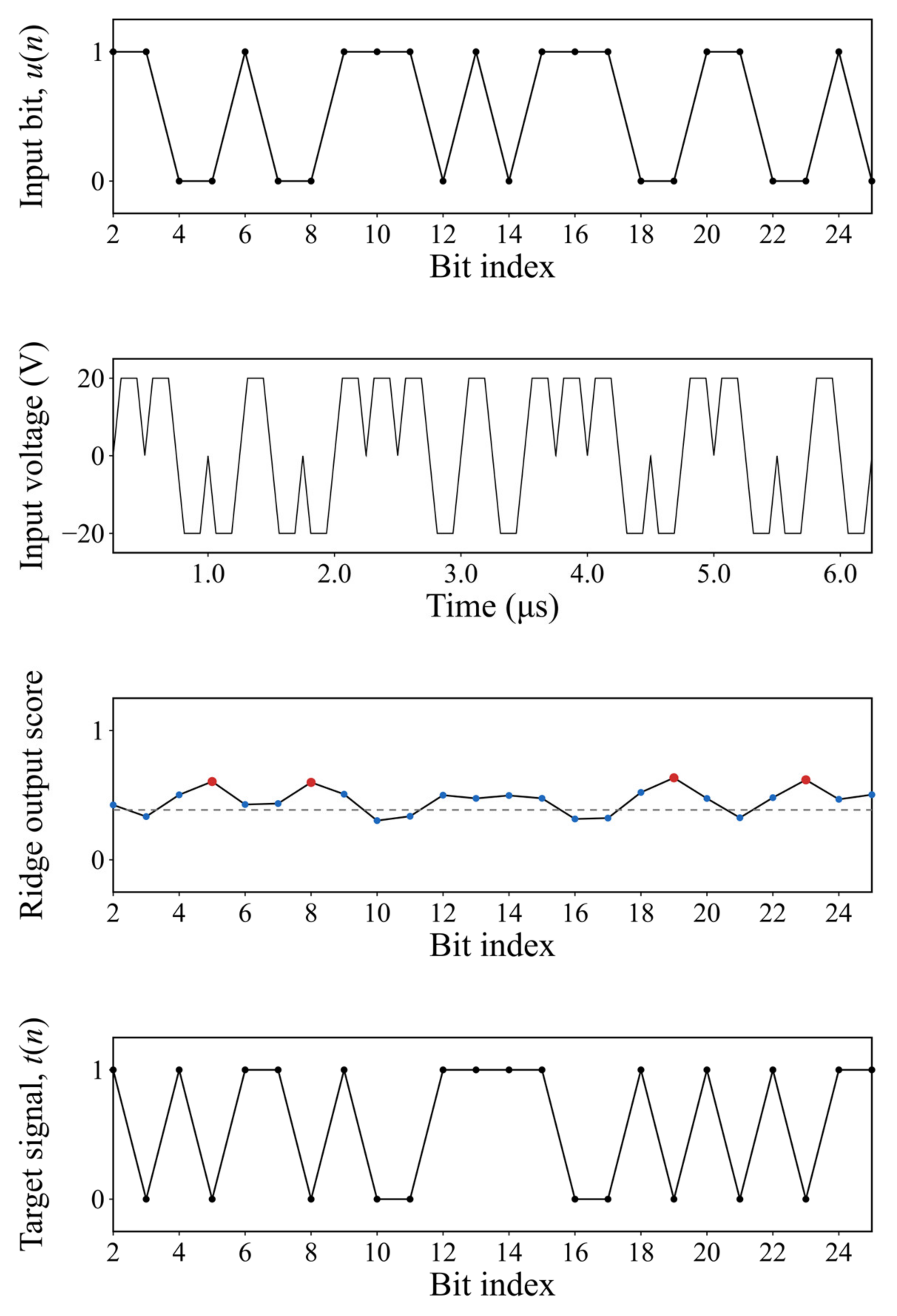
Two independently generated binary input sequences were prepared, and 120 labeled delayed-XOR samples were obtained from each sequence. The samples from the first sequence were used as the training set to determine the standardization parameters, PCA basis, Ridge weights, and classification threshold. The Ridge regularization parameter was fixed at α = 10−4. The trained model was then evaluated, without refitting or parameter adjustment, using the 120 samples from the second sequence. The model correctly classified 101 of these 120 independent test samples, corresponding to an accuracy of 84.2%.
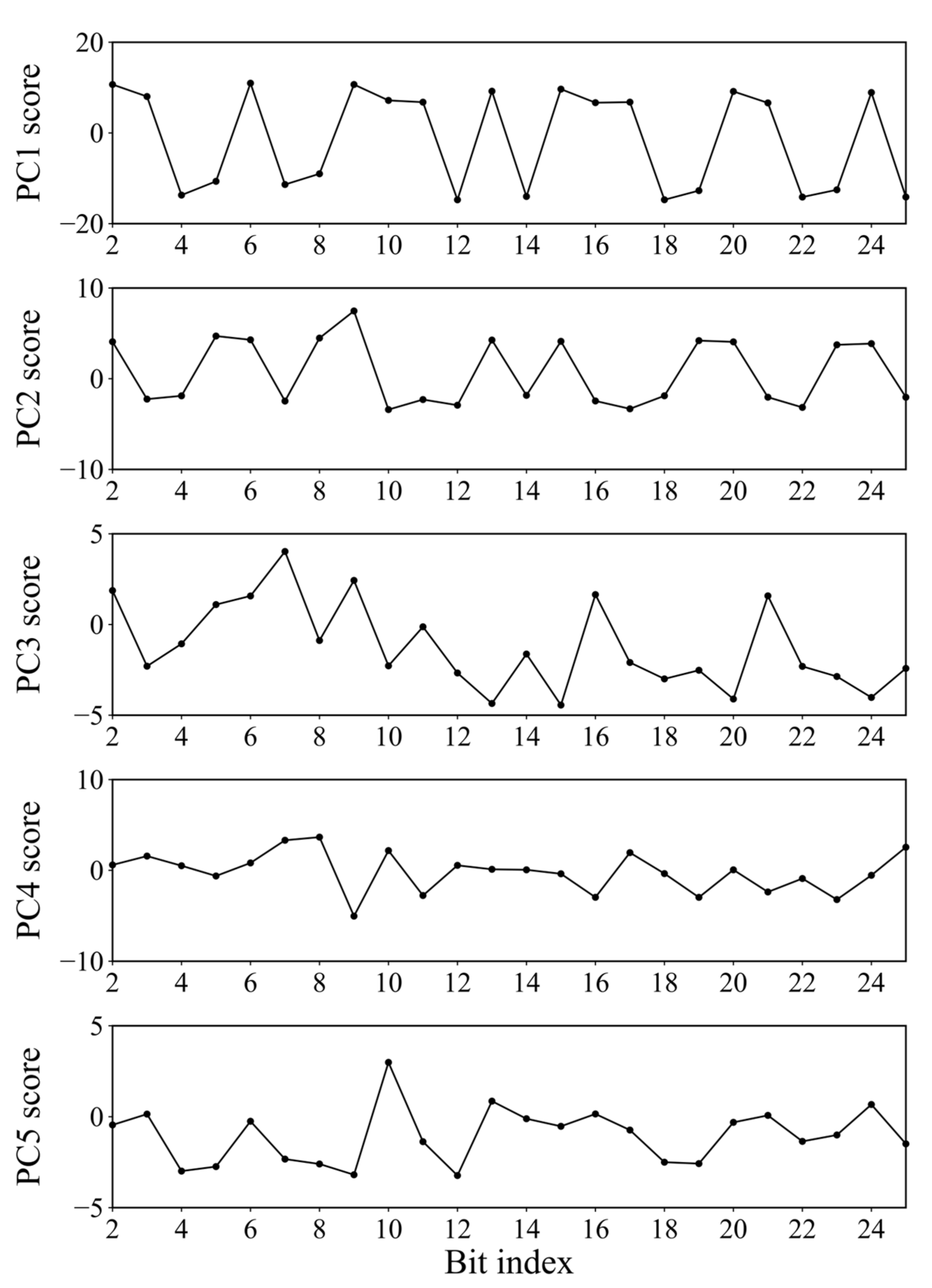
Figure A1 shows a representative 24-sample segment of the independent test sequence. The continuous Ridge output score was classified using the threshold determined from the training sequence. Figure A2 shows the corresponding variation across the test samples of the five PCA scores supplied to the Ridge readout.
Figure A1. Evaluation of the delayed-XOR task on a separately generated test sequence using the trained linear Ridge model without refitting. A representative 24-sample segment shows the input bit, corresponding input-voltage waveform, Ridge output score, and target XOR signal. The dashed line indicates the classification threshold determined from the training sequence. Blue and red markers denote correctly and incorrectly classified samples, respectively. The black dots in the input and target panels indicate the values at each bit index, and the lines connect adjacent values as guides to the eye.
Applsci 16 08506 g0a1
Figure A2. Five principal-component scores corresponding to the test samples shown in Figure A1. The PCA basis was determined using the 120 training samples and applied without modification to the separately generated test sequence.
Applsci 16 08506 g0a2

Appendix C. Network Dependence of Sine Waveform Generation
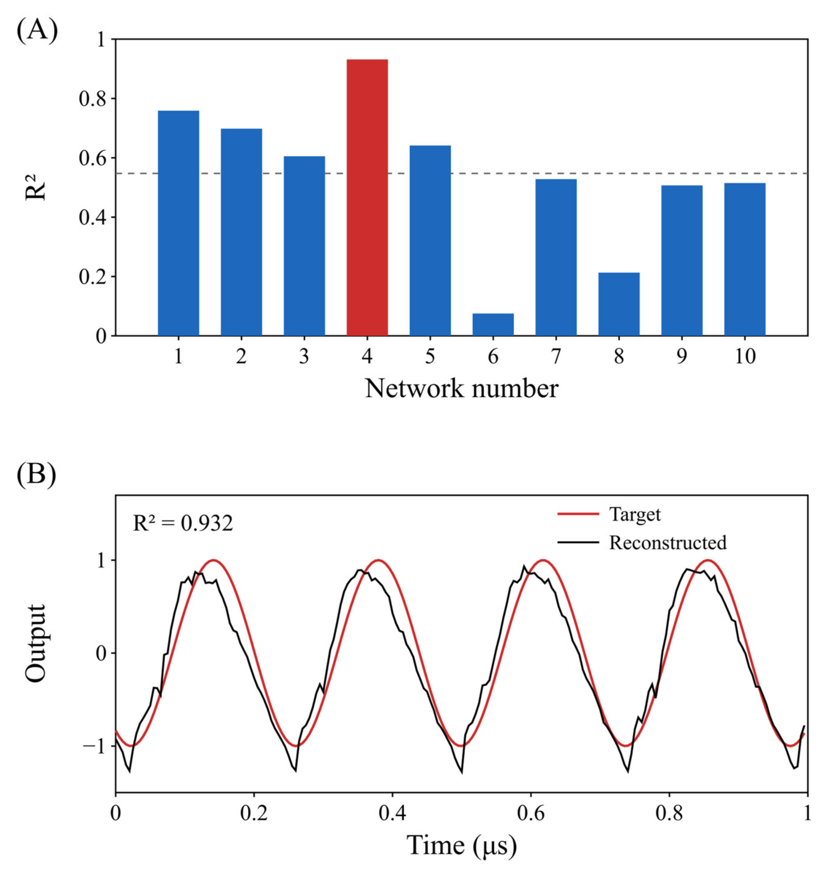
To examine the dependence of sine waveform reconstruction on network structure, ten network configurations were independently generated according to the network-construction procedure described in Section 2.3. Network numbers 1–10 correspond to network seeds 1001–1010, respectively, and each network contained 50 charge-storage nodes.
The circuit parameters, applied-voltage protocol, observation procedure, and linear readout were the same as those described in Section 4.2. For each network, a frequency shared among multiple observation currents was identified from the constant-voltage response, and the period of the target sine waveform was set to that network-specific frequency.
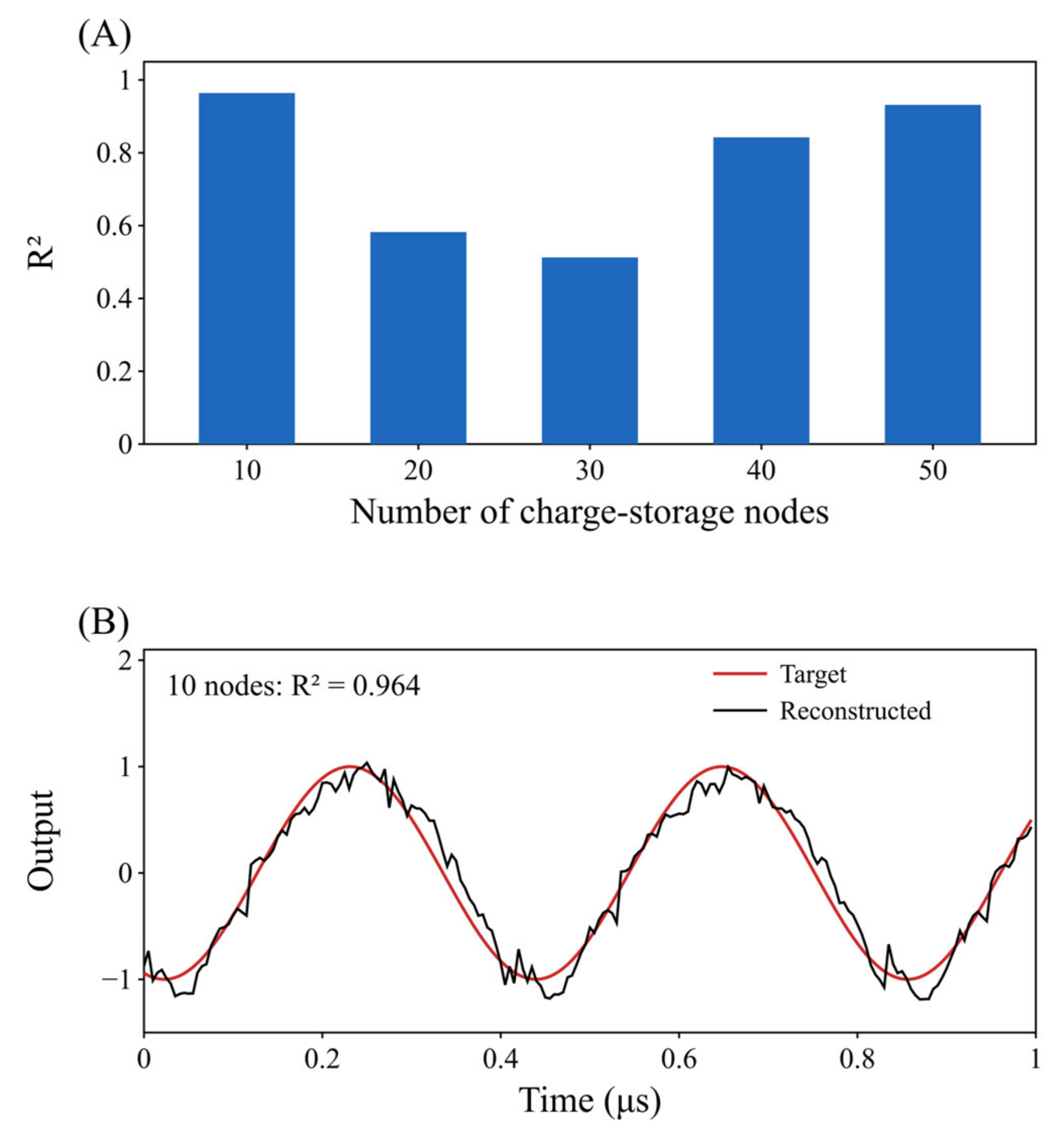
Figure A3A shows the reconstruction performance for the ten networks. The coefficient of determination ranged from 0.075 to 0.932, with a mean of 0.547 and a median of 0.567, demonstrating substantial network-to-network variation. Network 4 gave the highest value, R2 = 0.932. Figure A3B shows a 1 μs segment of its target and reconstructed waveforms.
Figure A3. (A) Coefficient of determination for sine waveform reconstruction in ten independently generated networks. The dashed line indicates the mean across the ten networks, and Network 4 is highlighted. (B) Target and reconstructed waveforms for Network 4 over a 1 μs interval.
Applsci 16 08506 g0a3
The influence of the number of charge-storage nodes was then examined using Network 4. Starting from the 50-node configuration, charge-storage nodes were progressively removed to obtain configurations containing 40, 30, 20, and 10 nodes. Edges from which the charge-storage nodes were removed were treated as simple resistor edges, while the underlying circuit was retained. When the 4.2 MHz target frequency identified for the 50-node network was applied unchanged, reconstruction was difficult for all reduced-node configurations (R2 < 0.025). When the target period was instead matched to the frequency identified for each node-count condition, the R2 values for 10, 20, 30, 40, and 50 nodes were 0.964, 0.582, 0.513, 0.842, and 0.932, respectively, as shown in Figure A4A. The dependence was nonmonotonic, and the 10-node configuration produced the highest value. Its target and reconstructed waveforms are shown in Figure A4B.
Figure A4. Dependence of sine waveform reconstruction on the number of charge-storage nodes in Network 4. (A) Coefficient of determination obtained after matching the target period to the frequency identified for each node-count condition. (B) Target and reconstructed waveforms for the 10-node configuration over a 1 μs interval.
Applsci 16 08506 g0a4

Appendix D. Time-Step Sensitivity

The sensitivity of the simulated response to temporal discretization was examined using time steps of 0.025, 0.05, 0.1, and 1 ns. The reference network, circuit parameters, and random-number seeds were held fixed. When the time step was changed, the voltage increment per step and the number of simulation steps were adjusted so that the voltage sweep rate and observation time remained unchanged.
As an order-of-magnitude reference, combining the representative resistance ratio R 0   / R * = 70 with C j / C * = 0.7 and 0.1 gives representative RC timescales of approximately 49 and 7 ns, respectively, using t * = R * C * = 1   n s . The adopted time step of 0.05 ns is therefore approximately 1/980 and 1/140 of these representative timescales, respectively.
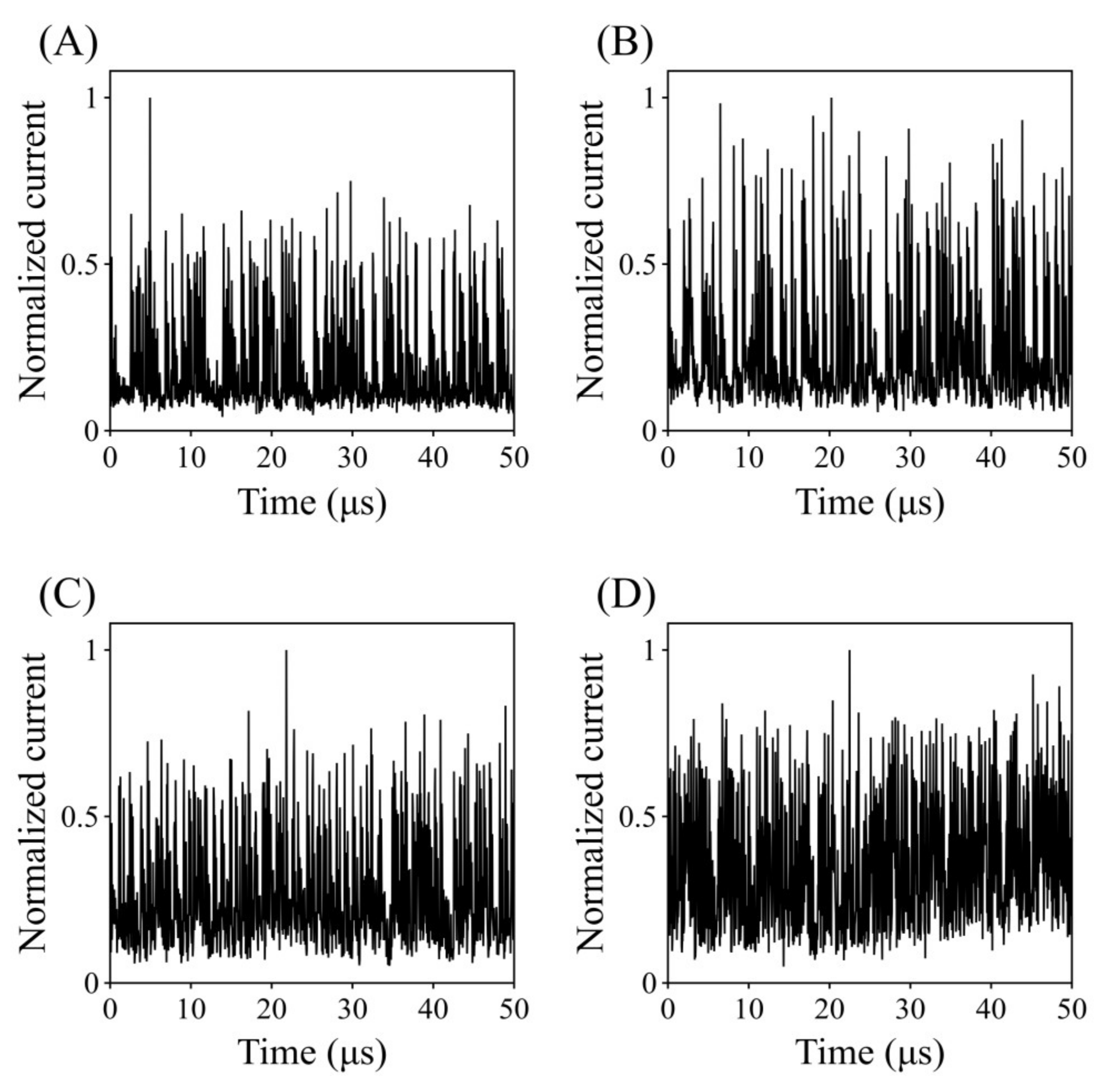
The constant-voltage comparison used the protocol of Figure 3: the voltage was swept from 0 to 40 V at 108 V/s and then held at 40 V for 50 μs. Figure A5 shows the temporal responses after the voltage reached 40 V. For visualization, the current-fluctuation amplitudes were normalized separately in each panel. Relative to the 0.025 ns calculation, the 0.05 ns calculation differed by 0.66% in mean current, 0.23% in current standard deviation, 0.66% in transferred charge, and 0.43% in time-averaged total charge in the charge-storage nodes over the 50 μs interval. Larger changes in the fluctuation and charge statistics were observed at the coarser time steps, particularly at 1 ns.
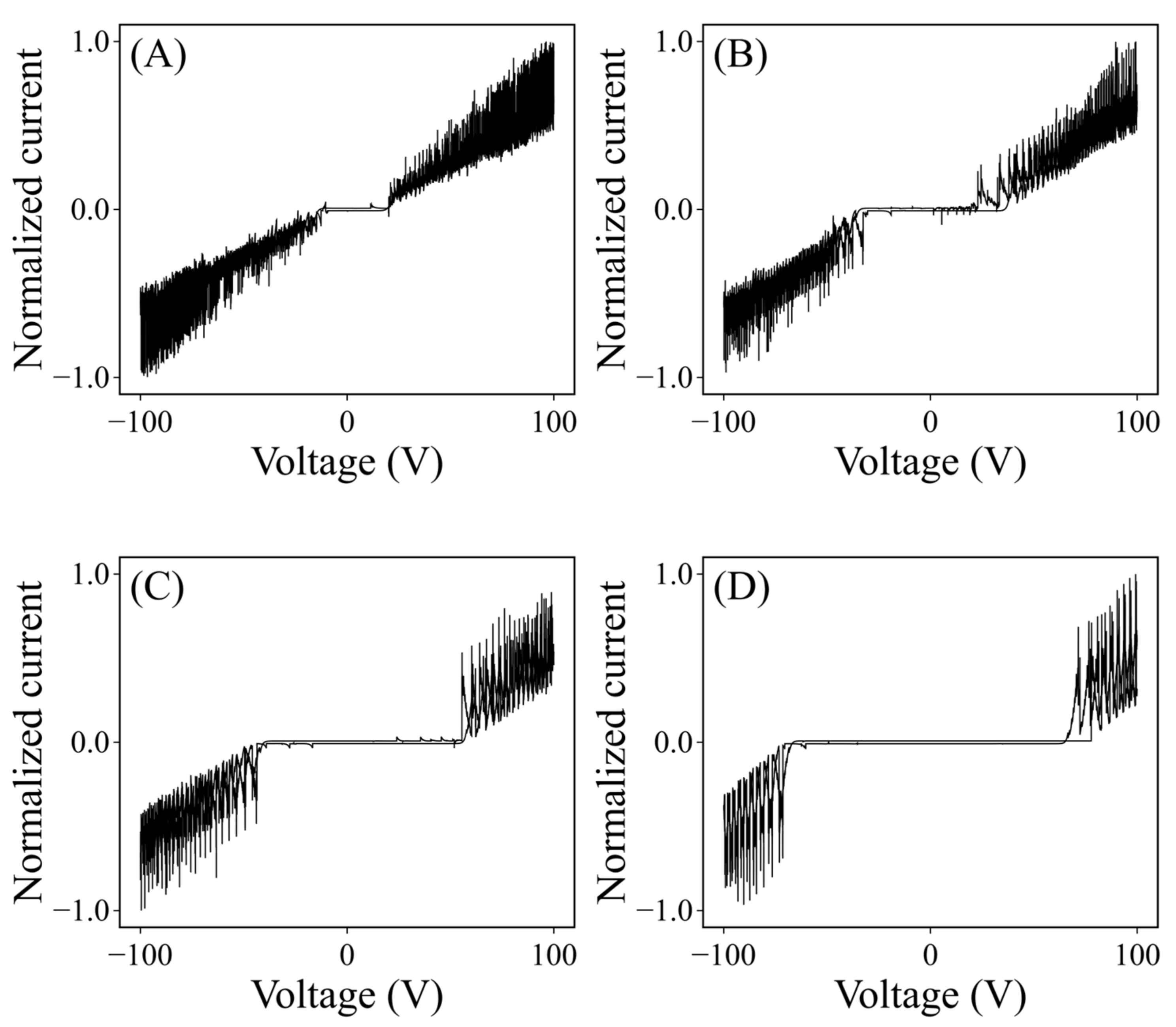
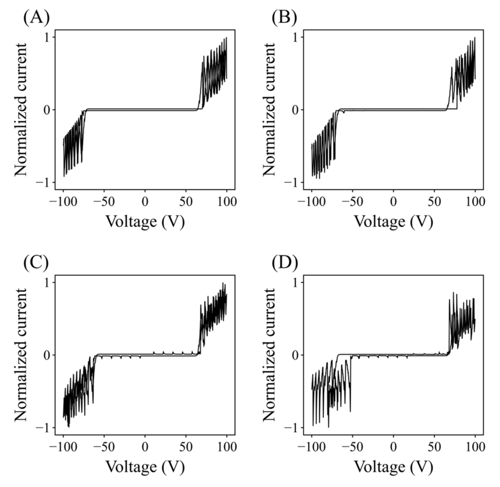
The I–V comparison used the condition shown in Figure 6C: C j / C * = 0.1 , a voltage range of ±100 V, and a sweep rate of 108 V/s. The initial sweep from 0 to +100 V was excluded, and only the two sweep segments following the first turning point are shown in Figure A6. The overall I–V shape, the low-current central region, and the high-voltage increase in current were retained when the time step was refined from 0.05 to 0.025 ns. Local differences were observed in the positions and amplitudes of individual current fluctuations, particularly on the negative-voltage side.
Refining the time step from 0.05 to 0.025 ns produced sub-1% differences in the principal constant-voltage statistics and retained the overall I–V response. However, changing the time step alters the sequence of stochastic tunneling evaluations and random-number consumption; therefore, even with the same random-number seed, early tunneling events and the subsequent threshold-triggered cascade-like responses may occur at different times. Accordingly, 0.05 ns was adopted as a practical compromise between temporal resolution and computational cost.
Figure A5. Time-step sensitivity of the temporal current response under a constant applied voltage. The voltage was swept from 0 to 40 V and then held at 40 V for 50 μs. The time step was (A) 0.025, (B) 0.05, (C) 0.1, and (D) 1 ns. Each panel was normalized separately.
Applsci 16 08506 g0a5
Figure A6. Time-step sensitivity of the I–V characteristics calculated using the condition shown in Figure 6C. The physical sweep rate was fixed at 108 V/s, and the voltage increment per step was adjusted with the time step. The initial sweep from 0 to +100 V was omitted. The time step was (A) 0.025, (B) 0.05, (C) 0.1, and (D) 1 ns. The current was normalized separately in each panel.
Applsci 16 08506 g0a6

References

  1. Dambre, J.; Verstraeten, D.; Schrauwen, B.; Massar, S. Information processing capacity of dynamical systems. Sci. Rep. 2012, 2, 514. [Google Scholar] [CrossRef] [Scilit]
  2. Kia, B.; Lindner, J.F.; Ditto, W.L. Nonlinear dynamics as an engine of computation. Philos. Trans. R. Soc. A 2017, 375, 20160222. [Google Scholar] [CrossRef] [Scilit]
  3. Jaeger, H.; Noheda, B.; van der Wiel, W.G. Toward a formal theory for computing machines made out of whatever physics offers. Nat. Commun. 2023, 14, 4911. [Google Scholar] [CrossRef] [Scilit]
  4. Tanaka, G.; Yamane, T.; Héroux, J.B.; Nakane, R.; Kanazawa, N.; Takeda, S.; Numata, H.; Nakano, D.; Hirose, A. Recent advances in physical reservoir computing: A review. Neural Netw. 2019, 115, 100–123. [Google Scholar] [CrossRef] [Scilit]
  5. Nakajima, K. Physical reservoir computing—An introductory perspective. Jpn. J. Appl. Phys. 2020, 59, 060501. [Google Scholar] [CrossRef] [Scilit]
  6. Stepney, S. Physical reservoir computing: A tutorial. Nat. Comput. 2024, 23, 665–685. [Google Scholar] [CrossRef] [Scilit]
  7. Nakajima, K.; Hauser, H.; Kang, R.; Guglielmino, E.; Caldwell, D.G.; Pfeifer, R. A soft body as a reservoir: Case studies in a dynamic model of octopus-inspired soft robotic arm. Front. Comput. Neurosci. 2013, 7, 91. [Google Scholar] [CrossRef] [Scilit]
  8. Nakajima, M.; Tanaka, K.; Hashimoto, T. Scalable reservoir computing on coherent linear photonic processor. Commun. Phys. 2021, 4, 20. [Google Scholar] [CrossRef] [Scilit]
  9. Lee, O.; Wei, T.; Stenning, K.D.; Gartside, J.C.; Prestwood, D.; Seki, S.; Aqeel, A.; Karube, K.; Kanazawa, N.; Taguchi, Y.; et al. Task-adaptive physical reservoir computing. Nat. Mater. 2024, 23, 79–87. [Google Scholar] [CrossRef] [Scilit]
  10. Newman, M.E.J. The structure and function of complex networks. SIAM Rev. 2003, 45, 167–256. [Google Scholar] [CrossRef] [Scilit]
  11. Diaz-Alvarez, A.; Higuchi, R.; Sanz-Leon, P.; Marcus, I.; Shingaya, Y.; Stieg, A.Z.; Gimzewski, J.K.; Kuncic, Z.; Nakayama, T. Emergent dynamics of neuromorphic nanowire networks. Sci. Rep. 2019, 9, 14920. [Google Scholar] [CrossRef] [Scilit]
  12. Bose, S.K.; Shirai, S.; Mallinson, J.B.; Brown, S.A. Synaptic dynamics in complex self-assembled nanoparticle networks. Faraday Discuss. 2019, 213, 471–485. [Google Scholar] [CrossRef] [Scilit]
  13. Hughes, K.J.; Iyer, K.A.; Bird, R.E.; Ivanov, J.; Banerjee, S.; Georges, G.; Zhou, Q.A. Review of carbon nanotube research and development: Materials and emerging applications. ACS Appl. Nano Mater. 2024, 7, 18695–18713. [Google Scholar] [CrossRef] [Scilit]
  14. Wang, H.; Hamanaka, S.; Nishimoto, Y.; Irle, S.; Yokoyama, T.; Yoshikawa, H.; Awaga, K. In operando X-ray absorption fine structure studies of polyoxometalate molecular cluster batteries: Polyoxometalates as electron sponges. J. Am. Chem. Soc. 2012, 134, 4918–4924. [Google Scholar] [CrossRef] [Scilit]
  15. Weinstock, I.A.; Schreiber, R.E.; Neumann, R. Dioxygen in polyoxometalate mediated reactions. Chem. Rev. 2018, 118, 2680–2717. [Google Scholar] [CrossRef] [Scilit]
  16. Tanaka, H.; Akai-Kasaya, M.; TermehYousefi, A.; Hong, L.; Fu, L.; Tamukoh, H.; Tanaka, D.; Asai, T.; Ogawa, T. A molecular neuromorphic network device consisting of single-walled carbon nanotubes complexed with polyoxometalate. Nat. Commun. 2018, 9, 2693. [Google Scholar] [CrossRef] [Scilit]
  17. Akai-Kasaya, M.; Igarashi, K.; Asai, T. Cellular automata models for reservoir computing in single-walled carbon nanotube network complexed with polyoxometalate. Nonlinear Theory Appl. IEICE 2024, 15, 17–35. [Google Scholar] [CrossRef] [Scilit]
  18. Grabert, H.; Devoret, M.H. (Eds.) Single Charge Tunneling: Coulomb Blockade Phenomena in Nanostructures; Plenum Press: New York, NY, USA, 1992. [Google Scholar]
  19. Akazawa, M.; Amemiya, Y.; Shibata, N. Annealing method for operating quantum-cellular-automaton systems. J. Appl. Phys. 1997, 82, 5176–5184. [Google Scholar] [CrossRef] [Scilit]
  20. Yamada, T.; Akazawa, M.; Asai, T.; Amemiya, Y. Boltzmann machine neural network devices using single-electron tunnelling. Nanotechnology 2001, 12, 60–67. [Google Scholar] [CrossRef] [Scilit]
  21. Watanabe, S.; Oya, T. Multiple-Electron Random Network System Simulation Based on Carbon Nanotube/Polyoxometalate Network. In Proceedings of the IEEE Silicon Nanoelectronics Workshop 2025 (SNW 2025), 10-05, Kyoto, Japan, 8–9 June 2025. [Google Scholar]
  22. Watanabe, S.; Oya, T. Potential of a Multiple-Electron Random Network for Reservoir Computing. In Proceedings of the IEEE Silicon Nanoelectronics Workshop 2026 (SNW 2026), P1-5, Honolulu, HI, USA, 13–14 June 2026. [Google Scholar]
  23. Borghi, M.; Biasi, S.; Pavesi, L. Reservoir computing based on a silicon microring and time multiplexing for binary and analog operations. Sci. Rep. 2021, 11, 15642. [Google Scholar] [CrossRef] [Scilit]
  24. Srikimkaew, O.; Banerjee, D.; Azhari, S.; Usami, Y.; Tanaka, H. High performance of an in-material reservoir computing device achieved by complex dynamics in a nanoparticle random network memristor. ACS Appl. Electron. Mater. 2024, 6, 688–695. [Google Scholar] [CrossRef] [Scilit]
  25. Wu, C.; Qiao, X.; Robertson, C.M.; Higgins, S.J.; Cai, C.; Nichols, R.J.; Vezzoli, A. A Chemically Soldered Polyoxometalate Single-Molecule Transistor. Angew. Chem. Int. Ed. 2020, 59, 12029–12034. [Google Scholar] [CrossRef] [Scilit]
  26. Volatron, F.; Izzet, G.; Vuillaume, D.; Proust, A. Unveiling Polyoxometalate Redox Properties at the Nanoscale. Comptes Rendus Chim. 2024, 27, 255–268. [Google Scholar] [CrossRef] [Scilit]
Figure 1. Conceptual mapping between the physical structure of the carbon nanotube/polyoxometalate (CNT/POM) network (top) and the proposed circuit model (bottom). CNTs are modeled as resistors R , the CNT–POM interfaces as tunnel junctions with capacitance C j , and the POM molecule as a charge-storage node. Arrows A and B indicate inward and outward electron transitions, respectively.
Applsci 16 08506 g001
Figure 2. An example of a multiple-electron random network constructed according to the procedure described in the text and placed between the left and right electrodes (yellow vertical lines), across which the external voltage is applied. The green outline indicates an enlarged view of a representative portion of a multiple-electron edge containing one charge-storage node. Twenty-five electrical nodes are arranged in five rows and five columns. In total, 10 of the 40 candidate internal edges are removed, leaving 30 internal edges. The five electrical nodes along each of the left and right edges are connected to the corresponding electrode through simple resistors. Charge-storage nodes are embedded along the multiple-electron edges. Series-connected resistive elements without an intervening electrical node are represented by a single equivalent resistor.
Applsci 16 08506 g002
Figure 3. Temporal current response under a constant applied voltage of 40 V. The voltage was first swept from 0 to 40 V and subsequently held at 40 V for 50 μs. The current response measured from 40 to 45 μs after the voltage reached 40 V is shown. The current was normalized by the maximum current value within the displayed interval.
Applsci 16 08506 g003
Figure 4. Simulated I–V characteristics of the multiple-electron random network at different voltage sweep rates: (A) 107, (B) 2 × 10⁷, (C) 5 × 10⁷, and (D) 108 V/s.
Applsci 16 08506 g004
Figure 5. Simulated I–V characteristics with (A) 0, (B) 10, (C) 30, and (D) 50 charge-storage nodes. The 50-node configuration corresponds to the reference network, and the smaller configurations were generated by progressively removing charge-storage nodes while retaining the underlying circuit structure. The initial sweep from 0 to +20 V is omitted, and only the subsequent sweep segments are shown. The orange arrows indicate the voltage-sweep direction.
Applsci 16 08506 g005
Figure 6. Simulated I–V characteristics of the reference network containing 50 charge-storage nodes for junction capacitances of C j / C * = (A) 0.7, (B) 0.3, and (C) 0.1 at a voltage sweep rate of 108 V/s. The initial sweep from 0 V to the positive-voltage turning point is omitted, and only the subsequent sweep segments are shown.
Applsci 16 08506 g006
Figure 7. Simulated I–V characteristics for β = (A) −2, (B) −1, (C) 0, (D) 0.2, (E) 1, and (F) 2. C j / C * = 0.1, Q t h = 20, and the voltage sweep rate of 108 V/s were held fixed. The initial sweep from 0 to +100 V is omitted, and only the subsequent sweep segments are shown.
Applsci 16 08506 g007
Figure 8. Simulated I–V characteristics for Q t h   = (A) 5, (B) 10, (C) 15, and (D) 20 electrons. C j / C * = 0.1, β = 0.2, and the voltage sweep rate of 108 V/s were held fixed. The initial sweep from 0 to +100 V is omitted, and only the subsequent sweep segments are shown.
Applsci 16 08506 g008
Figure 9. Delayed XOR task. The figure shows the binary input sequence, the corresponding input voltage, the network response, the normalized integrated output, and the target signal. The first input interval was excluded to avoid the initial transient and because no preceding bit was available for defining the delayed-XOR target. The black dots indicate the values at each bit index, and the lines connect adjacent values as guides to the eye.
Applsci 16 08506 g009
Figure 10. Classification of the delayed XOR task using the normalized integrated output. The dashed line indicates the threshold used to distinguish the two output classes.
Applsci 16 08506 g010
Figure 11. Sine waveform generation from a constant voltage input. The figure shows the input voltage, the untrained output obtained using uniform readout weights, the reconstructed output after Ridge regression, and the target sine waveform. The network states were obtained by averaging the 20 observation currents over 5 ns intervals.
Applsci 16 08506 g011
Disclaimer/Publisher’s Note: The statements, opinions and data contained in all publications are solely those of the individual author(s) and contributor(s) and not of MDPI and/or the editor(s). MDPI and/or the editor(s) disclaim responsibility for any injury to people or property resulting from any ideas, methods, instructions or products referred to in the content.