Article

Freewheeling Diode Current Under Open-Phase Fault in Field-Weakening Region of Multiple Three-Phase Drives

by
Živa Stare
*,
Henrik Lavrič
,
Mitja Nemec
and
Klemen Drobnič
University of Ljubljana, Faculty of Electrical Engineering, Tržaška cesta 25, SI-1000 Ljubljana, Slovenia
*
Author to whom correspondence should be addressed.
Appl. Sci. 2026, 16(12), 5994; https://doi.org/10.3390/app16125994
Submission received: 15 May 2026 / Revised: 9 June 2026 / Accepted: 11 June 2026 / Published: 13 June 2026
(This article belongs to the Special Issue Reliability and Fault Tolerant Control of Electric Machines)

Abstract

Multiple three-phase machine drives are inherently fault-tolerant due to their multiphase structure; however, they remain susceptible to inverter-related faults. A common fault is the loss of gate signals in one inverter leg, resulting in an open-phase condition. Under such conditions, a reverse conduction path is established through the freewheeling diodes of the faulted leg, leading to uncontrolled freewheeling diode current generation. The resulting freewheeling diode current becomes particularly critical in the field-weakening region, when the back-EMF may exceed the DC-link voltage and a large reverse current can occur. This paper derives an analytical expression for real-time prediction of the freewheeling diode current in a triple three-phase surface-mounted permanent magnet synchronous machine drive. The method is applicable in both the constant-torque and field-weakening regions. The analytical prediction is validated through comparison with both experimentally measured and numerically simulated freewheeling diode current waveforms over a wide range of operating points, including no-load and loaded conditions. The results show that the proposed model accurately reproduces the envelope and conduction boundaries, while maintaining good agreement with simulations and measurements. The predicted current can be utilized in post-fault control, fault detection, and sensorless position estimation.

1. Introduction

Multiphase machine drives are often associated with enhanced safety due to their inherent fault tolerance, which arises from their structure comprising more than three phases [1]. Among the various multiphase topologies, multiple three-phase machine drives, composed of several isolated three-phase winding sets, represent a practical and widely adopted solution [2]. Each winding set can be treated as an independent three-phase machine, allowing the use of well-established control strategies [3,4,5] and conventional power supply technologies [6], while improving fault tolerance and modularity [7].
In addition to enhanced reliability, multiphase topologies offer further advantages, including reduced torque ripple, increased power density, and improved thermal distribution [8]. These characteristics make them particularly attractive for high-performance and safety-critical applications such as electric vehicles [9,10], marine propulsion systems [11,12,13], and wind power generation [14,15,16].
Despite these advantages, multiphase drives are not immune to faults, and those occurring in the power inverter account for a significant proportion of all drive malfunctions [17,18]. Among inverter-related faults, switching device faults are the most common and may arise due to device degradation, driver malfunctions, or protection-triggered shutdowns [19].
This paper focuses on open-phase faults, i.e., the omission of gate signals in both switching devices in one of the inverter legs, while the freewheeling diodes remain operational [17]. Under such conditions, the affected phase is no longer actively controlled, but a current path is still maintained through the freewheeling diodes. This fault has a particularly strong impact when the drive operates in a field-weakening (FW) region [20]. In such conditions, a reversed conduction path is established through the freewheeling diodes, which can lead to uncontrolled generation of a large current flowing from the machine back into the power converter [21]. This phenomenon leads to increased electrical and thermal stress on the power electronic components, which can accelerate degradation, reduce service lifetime, and potentially result in inverter failure [22].
Recent research [17,23,24,25] has shown that under inverter open-phase faults with functional freewheeling diodes, a non-zero phase current persists because these diodes continue to provide a conduction path. This current is primarily driven by the phase back-EMF and occurs only during specific pulse width modulation (PWM) switching states. Based on this phenomenon, analytical models have been developed to describe the conduction mechanism and enable real-time prediction of the residual diode current by identifying conduction conditions, switching-state-dependent conduction intervals, and corresponding equivalent circuits [23]. These models have been further extended to relate freewheeling diode current (FDC) to back-EMF, often using simplified or piecewise-linear formulations, enabling applications such as fault diagnosis [17] and postfault sensorless control [25]. Moreover, analytical prediction of FDC has also been demonstrated in multiphase machines, including dual three-phase permanent magnet synchronous machines, confirming that such approaches are not limited to conventional three-phase drives [24]. Nevertheless, the existing approaches remain limited in several aspects: operation in the FW region is not addressed [17,23,24,25], switching-state-dependent conduction conditions are simplified or neglected in the multiphase case [24], favorable DC-link conditions are assumed [24], and accurate FDC acquisition requires sampling synchronized with the switching states [17,25]. These limitations reduce the applicability of existing FDC models to practical multiple three-phase drives operating over a wide speed range.
To address these limitations, this paper proposes an analytical method for predicting the FDC in a triple three-phase surface-mounted permanent magnet synchronous machine with weakly magnetically coupled winding sets (3 × 3PMSM). In contrast to previous studies [17,23,24,25], the proposed formulation remains valid in both the constant-torque and FW regions, explicitly accounts for switching-state-dependent conduction conditions, and does not rely on restrictive assumptions concerning operating conditions or DC-link dimensioning. In addition, instead of using additional sampling mechanisms synchronized with switching states for accurate current measurement, the proposed method analytically compensates for sampling-induced errors by correcting the initial condition of the FDC differential equation. This eliminates the need for additional switching-synchronized sampling which significantly reduces computational complexity. Although derived for a triple three-phase machine, the method can be extended to machines with any number of phases that is a multiple of three.

2. Analytical Modeling in Field-Weakening Region

This section develops the analytical model used to predict the FDC under an inverter open-phase fault in the FW region, as shown in Figure 1. First, the phase-domain voltage model of the 3 × 3PMSM drive is formulated to explicitly represent the faulted phase leg and diode conduction paths. Based on this model, the analytical expressions for the FDC are then derived for both possible conduction states.

2.1. Phase Voltages in Field-Weakening Region

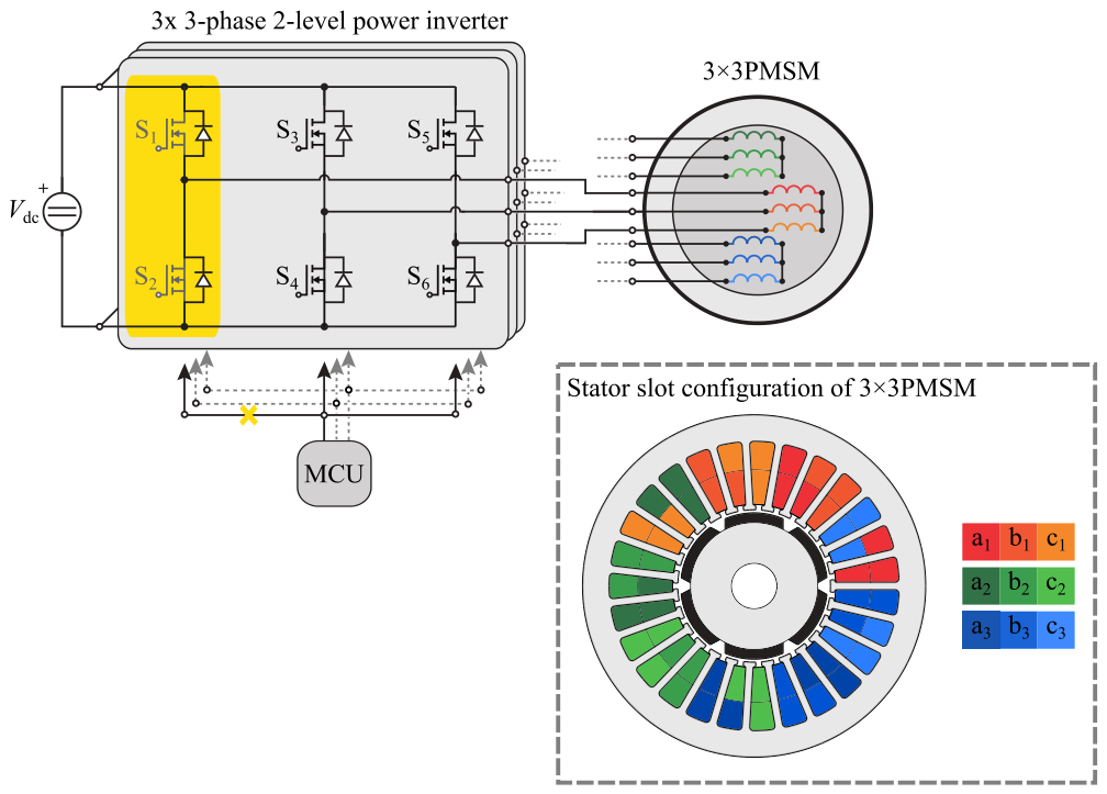
The model of the 3 × 3PMSM drive is depicted in Figure 1. The configuration consists of three distinct winding sets (indexed as 1, 2, and 3), each comprising three phases ( a , b , c ) connected to an isolated neutral point. These sets are electrically aligned and characterized by weak magnetic coupling between them.
The drive is modeled in the phase domain to account for the stationary nature of inverter-related open-phase faults. This enables direct modeling of the faulted phase leg and associated freewheeling diode conduction. In contrast, a rotating reference frame (e.g. dq-domain) would redistribute the fault-induced asymmetry across all three phases in the faulted inverter and obscure the physical interpretation of the conduction paths [23].
Accordingly, the machine is described by the phase-voltage equations and the corresponding flux–current relations,
v s = R s i s + d d t ψ s ,
ψ s = L s i s + ψ pm .
Vector v s = v a 1 , v b 1 , v c 1 , v a 2 , v b 2 , v c 2 , v a 3 , v b 3 , v c 3 T is the vector of stator voltages. The vectors of stator currents i s and flux linkages ψ s are defined correspondingly. The matrix R s = diag ( R s ) represents the stator phase winding resistance diagonal matrix, where all resistances are equal to R s , as it is assumed that all phase windings are identical.
Magnetic saturation is neglected, and L s is a constant asymmetric circulant inductance matrix,
L s = circ L s , L m 1 , L m 2 , L m 2 , L m 2 , L m 2 , L m 2 , L m 2 , L m 1 ,
where L s denotes phase self-inductance, L m 1 is the mutual inductance between phases that share a stator slot, and L m 2 is the mutual inductance between phases that do not share a stator slot in the analysed 3 × 3PMSM. The constant-inductance representation is considered appropriate for the surface-mounted permanent magnet synchronous machine (surface-mounted PMSM) analysed in this work. In a surface-mounted PMSM, the inherently large effective air gap significantly mitigates the armature reaction, thereby providing intrinsic immunity to magnetic saturation and cross-saturation effects [26,27,28]. The unconventional phase windings’ distribution to stator slots is illustrated in the bottom part of Figure 1.
Vector ψ pm represents rotor flux linkage, and its time derivative is equal to the back-EMF phase voltage
d d t ψ pm = E = Ψ pm ω e [ sin ( θ e ) sin ( θ e 2 π 3 ) sin ( θ e 4 π 3 ) sin ( θ e ) sin ( θ e 2 π 3 ) sin ( θ e 4 π 3 ) sin ( θ e ) sin ( θ e 2 π 3 ) sin ( θ e 4 π 3 ) ] ,
where Ψ pm is the constant permanent magnet flux linkage in the air-gap, ω e is the electrical angular velocity, and θ e is the rotor electrical angle.
As the FW region is analysed, it is also necessary to consider the reduction of flux linkage in the air-gap to increase angular velocity beyond the base speed. In 3 × 3PMSM, this is achieved by forcing the i d , ref < 0 command [29]. As a result, the back-EMF voltage in, e.g., phase a 1 is defined as
E a 1 = Ψ pm + L d i d 1 ω e sin ( θ e ) ,
where i d 1 is the d-axis stator current for the first winding set and L d is the d-axis stator inductance, calculated from three-phase Clarke and Park transforms.

2.2. Analytical Expression of the Freewheeling Diode Current

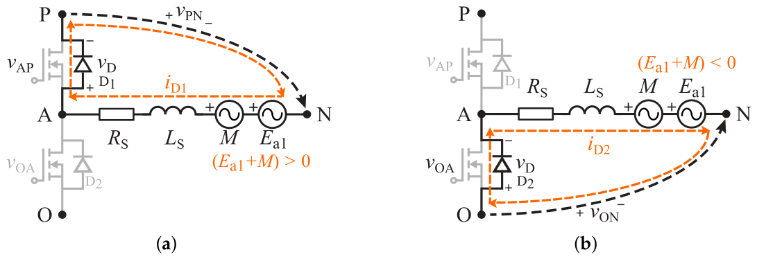
The possible conduction paths of the FDC are shown in Figure 2. Without loss of generality, it is assumed that the open-phase fault, i.e., the omission of the transistors’ gate signals, occurs in phase a of the first winding set. The FDC is defined as the current flowing through the upper or lower freewheeling diode in the faulted inverter leg under the open-phase fault. Therefore, the phase current in the faulted phase, i a 1 , is hereafter denoted as the freewheeling diode current i D , with the positive direction defined from the inverter to the machine.
Depending on its polarity, i D can flow through one of two conduction paths. For negative current polarity, the current conducts through the upper freewheeling diode D 1 , and the corresponding FDC is denoted as i D 1 (Figure 2a). For positive current polarity, it conducts through the lower freewheeling diode D 2 , and the corresponding FDC is denoted as i D 2 (Figure 2b). The overall FDC is therefore expressed as
i D = i D 1 + i D 2 ,
where only one current component is nonzero at a given instant, depending on which freewheeling diode is conducting.
The analytical expression for the FDC is first derived for conduction through the upper freewheeling diode D 1 , i.e., for i D 1 . From the equivalent circuit in Figure 2a, Kirchhoff’s law gives
v D + v PN E a 1 M L s d i D 1 d t R s i D 1 = 0 ,
where v D is defined as the diode forward voltage and v PN is a voltage difference between the positive terminal of the DC link and the isolated neutral point of the faulted winding set N. Values of v PN are determined in Section 3.3. Voltage E a 1 is the back-EMF voltage induced in the faulted phase due to the other phases in the machine that can still generate a rotating magnetic field. Since the FDC has the opposite polarity from E a 1 + M , conducting through D 1 occurs when E a 1 + M > 0 . The symbol M represents the sum of the time derivatives of the products of the healthy phases’ currents and their corresponding mutual inductances
M = L m 1 d i b 1 d t + L m 2 d i c 1 d t + L m 2 d i a 2 d t + L m 2 d i b 2 d t + L m 2 d i c 2 d t + L m 2 d i a 3 d t + L m 2 d i b 3 d t + L m 1 d i c 3 d t .
Solving the first-order differential equation derived from Equation (7) yields the expression for i D 1 ,
i D 1 t = I 0 · e t L s / R s + v PN + v D E a 1 + M R s · 1 e t L s / R s ,
where I 0 is the initial condition and will be defined in Section 4.2.
Similarly, for the lower freewheeling diode D 2 , i.e., for i D 2 , the conduction occurs when E a 1 + M < 0 . The Figure 2b shows the equivalent circuit and it is defined as
R s i D 2 + L s d i D 2 d t + M + E a 1 v ON + v D = 0 ,
and the solution for i D 2 is
i D 2 t = I 0 · e t L s / R s + v ON v D E a 1 + M R s · 1 e t L s / R s ,
where v ON is a voltage difference between the negative terminal of the DC link and the isolated neutral point of the faulted winding set N. Values of v ON are determined in Section 3.3.
Equations (9) and (11) are formulated in continuous time; however, due to the discrete switching nature of the inverter, they are applied piecewise over the individual PWM states within each switching period. The corresponding diode-conduction conditions are defined in the following section within a discrete-time formulation suitable for digital control implementation.

3. Conduction Conditions

This section first establishes the general conduction rule for the freewheeling diodes in the faulted inverter leg by relating diode conduction to the polarity and magnitude of E a 1 + M . The analysis then focuses on the post-fault interval before the freewheeling diode conduction begins, in order to determine which post-fault voltage vectors produce suitable values of v PN and v ON and therefore allow either D 1 or D 2 to conduct. Once the conduction intervals are identified, the values of v PN and v ON after diode conduction has started are determined, as these voltages are required in the analytical expressions for the FDC.

3.1. General Conduction Rule for the Freewheeling Diode Current

When E a 1 + M > 0 (Figure 2a), D 1 can conduct, while D 2 is reverse-biased by the voltage difference between the positive sum of E a 1 and M and the negative terminal of the DC link. From Figure 2a, D 1 can conduct if the voltage difference v AP is higher than v D ,
v AP = v a 1 v PN = E a 1 + M v PN > v D .
Before D 1 starts conducting, the current in the faulted phase is zero. Consequently, the voltage of the faulted phase is determined only by the induced back-EMF and the mutual coupling effects, i.e., v a 1 = E a 1 + M . The conduction condition in Equation (12) therefore does not include voltage terms induced by the i D 1 , since the FDC has not yet started to flow [17,23].
Similarly, when E a 1 + M < 0 (Figure 2b), diode D 2 can conduct and D 1 is reverse-biased by the voltage difference between the negative sum of E a 1 and M, and the positive terminal of the DC link
v OA = v ON v a 1 = v ON E a 1 + M > v D .
The values of v PN and v ON depend on which of the other healthy phases are connected to the positive or negative terminal of the DC-link and will be determined in Section 3.2. Therefore, the freewheeling diode can start conducting before the back-EMF induced voltage is higher than the DC-link voltage V dc , i.e., it can start conducting at speeds below the FW region [17].

3.2. Effect of Post-Fault Voltage Vectors on v PN and v ON Before Diode Conduction

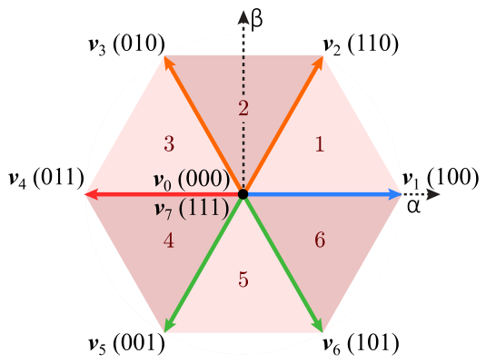
In Equations (12) and (13), the voltages v PN and v ON are among the quantities that determine whether diodes D 1 and D 2 can begin conducting. Hence, their values must be known in order to determine which freewheeling diode conducts. The analysis is based on the switching states of space vector pulse width modulation (SVPWM), and the corresponding voltage vectors are shown in Figure 3. The figure also indicates the SVPWM voltage sectors, which divide the space-vector plane into regions bounded by adjacent active voltage vectors. Within each sector, the reference voltage vector is synthesized using the two neighbouring active vectors and the zero vectors [30].
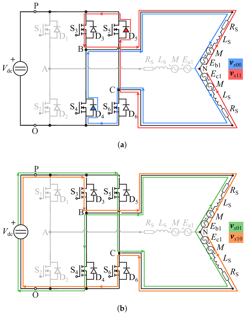
During an open-phase fault, the gate signals for the affected phase become invalid, reducing the number of available SVPWM switching states in a three-phase two-level inverter from eight to four [17,23]. Consequently, pairs of post-fault voltage vectors (PFVVs) whose SVPWM switching sequences differ only in the state of the faulted phase share the same conduction path and are hereafter represented by common notation, such as v x 00 for v 0 and v 1 . This grouping is applied to all PFVVs and is summarized in Table 1. The equivalent circuits corresponding to the four resulting post-fault switching states are illustrated in Figure 4 and the following conditions hold:
  • Since the 3 × 3PMSM has electrically isolated winding sets, the phase currents within each set must sum to zero under both healthy and faulty conditions [24]:
    i a k + i b k + i c k = 0 ,
    where k { 1 , 2 , 3 } denotes the respective winding set.
  • In the faulted winding set, i a 1 = 0 , consequently, the remaining phase currents are equal and opposite i b 1 = i c 1 .
  • The voltage of the faulted phase is defined by the sum of its back-EMF and the mutual coupling effects
    v a 1 = E a 1 + M .
  • The voltages for the healthy phases are calculated the same as under healthy conditions (Equation (1)).
  • Based on Equation (14), it follows that the sum of the three phase voltages within a single winding set must also be zero under all operating conditions [17]
    v a 1 + v b 1 + v c 1 = E a 1 + M + v b 1 + v c 1 = 0 .
Building on these statements and the equivalent circuits shown in Figure 2 and Figure 4, the conduction conditions for the freewheeling diodes can be established. Specifically, the voltages v PN and v ON are determined and subsequently applied to evaluate the FDC as defined in Equations (12) and (13).

3.2.1. Conduction Intervals for the Freewheeling Diode D 1

In both cases of Figure 4a, the healthy phases b 1 and c 1 are connected to the same rail of the DC link, so the line-to-line voltage is v b 1 c 1 = v b 1 v c 1 = 0 . Applying this to Equation (16) and assuming E a 1 + M > 0 , their phase voltages can be expressed as
v b 1 = v c 1 = E a 1 + M 2 .
If v x 11 is applied to the inverter, the voltage v PN = v b 1 = v c 1 = E a 1 + M / 2 . The conduction condition (12) is transformed to
v AP = 3 E a 1 + M 2 > v D .
The condition (18) means that v x 11 allows the conduction of i D 1 , when the positive sum of back-EMF voltage and mutual coupling effect in the faulted phase is higher than 2 v D / 3 .
Comparatively, if v x 00 is applied to the inverter and E a 1 + M > 0 , the voltage v ON = v b 1 = v c 1 = E a 1 + M / 2 . Since v PO denotes the voltage from the positive to the negative DC-link terminal, i.e., v PO = V dc , it follows that
v PN = v PO + v ON = V dc E a 1 + M 2 .
Applying Equation (19) to conduction condition (12),
v AP = 3 E a 1 + M 2 V dc 2 > v D .
The condition (20) means that v x 00 allows the conduction of i D 1 , when the positive E a 1 + M in the faulted phase is higher than 2 ( V dc + v D ) / 3 . However, this voltage condition cannot be reached with a three-phase two-level inverter in standard conditions [23]. Hence, v x 00 does not allow current conduction through D 1 , when E a 1 + M > 0 .
Similarly, the analysis for the conduction conditions for the freewheeling diode D 1 can be done for the PFVVs in Figure 4b. In the case of PFVV v x 10 , the line-to-line voltage is v b 1 c 1 = v b 1 v c 1 = V dc and by substituting it into Equation (16), we obtain phase voltage v b 1 , which is equal to v PN ,
v b 1 = V dc E a 1 + M 2 = v PN .
Substituting v PN in Equation (12) with Equation (21), the conduction condition becomes
v AP = 3 E a 1 + M V dc 2 > v D
Thus, the conduction (22) occurs if E a 1 + M > ( V dc + 2 v D ) / 3 . The conduction condition is the same if v x 01 is applied and phase voltage
v c 1 = V dc E a 1 + M 2 = v PN .
Hence, both PFVVs in Figure 4b can activate i D 1 if E a 1 + M > ( V dc + 2 v D ) / 3 .

3.2.2. Conduction Intervals for the Freewheeling Diode D 2

The analysis is extended to the conduction of the freewheeling diode D 2 in a similar way. The main differences are the polarity of E a 1 + M , as the conduction via D 2 is only possible if E a 1 + M < 0 (Figure 2b) and the conduction condition is expressed as Equation (13).
Applying v x 00 (Figure 4a, blue line) means that v ON = v b 1 = v c 1 = E a 1 + M / 2 and the condition in Equation (13) is
v OA = 3 E a 1 + M 2 > v D .
The condition (24) means that v x 00 allows the conduction of i D 2 , when the negative sum E a 1 + M in the faulted phase is lower than 2 v D / 3 .
Applying v x 11 (Figure 4a, red line) means that v PN = v b 1 = v c 1 = E a 1 + M / 2 . Since v OP denotes the voltage from the negative to the positive DC-link terminal, i.e., v OP = V dc , the voltage v ON equals
v ON = v OP + v PN = V dc E a 1 + M 2 .
The condition in Equation (13) is
v OA = 2 V dc + 3 E a 1 + M 2 > v D .
The condition (26) means that v x 11 does not allow the conduction of i D 2 , as the negative sum E a 1 + M in the faulted phase would have to be lower than 2 ( V dc + v D ) / 3 .
In Figure 4b, v x 01 corresponds to
v ON = v b 1 = V dc E a 1 + M 2
and v x 10 to
v ON = v c 1 = V dc E a 1 + M 2 .
The conduction condition is the same for v x 01 and v x 10 and is equal to
v OA = V dc + 3 E a 1 + M 2 > v D .
Hence, both PFVVs in Figure 4b can activate i D 2 if E a 1 + M < ( V dc + 2 v D ) / 3 .
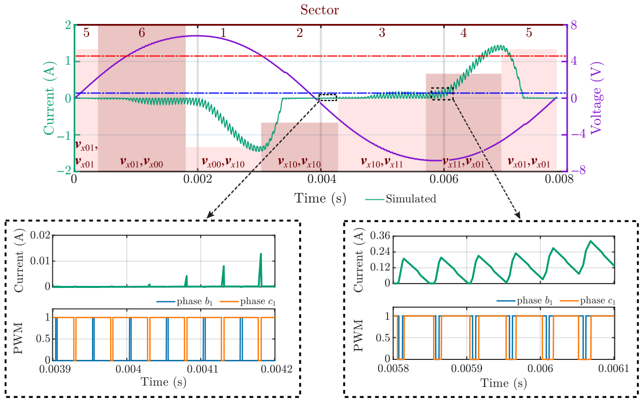
All of the conduction intervals are summarized and illustrated in Figure 5. The plot on the top shows one electrical period of the simulated FDC in the FW region together with the corresponding E a 1 + M , while the simulation model is described in Section 4.3. The blue and red lines indicate the conduction boundaries defined by conditions (18) and (22), respectively. At the beginning of the shown interval, E a 1 + M is below the first conduction boundary, indicated by the blue line, and therefore neither freewheeling diode conducts.
As E a 1 + M exceeds the first conduction boundary, i D 1 starts to flow. Initially, its amplitude is small because both active vectors in Sector 6 are non-conducting vectors for i D 1 . In this region, i D 1 can conduct only during v x 11 , which corresponds to one of the zero-vector states and is applied only for short intervals within the SVPWM sequence. When E a 1 + M reaches the second conduction boundary, indicated by the red line, v x 01 also becomes a conducting vector and the amplitude of i D 1 increases due to the longer conduction interval. At the boundary between Sectors 6 and 1, the amplitude decreases because the dominant vector is v x 00 , which does not conduct i D 1 . Deeper into Sector 1, v x 10 becomes increasingly dominant, causing the amplitude of i D 1 to rise again. The maximum amplitude is reached near the end of Sector 1. Once E a 1 + M falls below the second conduction boundary, the amplitude rapidly decreases because the dominant vectors in Sector 2 are non-conducting for i D 1 under this condition.
The same reasoning applies to the second half of the electrical period, where the conduction of i D 2 occurs. The two enlarged windows on the bottom of Figure 5 highlight different stages of the FDC current evolution. The left window shows the beginning of the FDC conduction; the current i D 2 starts to conduct at the time instant t = 0.004028   s , when E a 1 + M decreases below the conduction boundary defined by Equation (24). At this instant, FDC conduction occurs while the PFVV v x 00 is applied, since it is a conducting vector for i D 2 . The right window shows the later current evolution, after E a 1 + M has decreased below the conduction boundary defined with Equation (29), when the only non-conducting PFVV is v x 11 .

3.3. Determination of v PN and v ON After Diode Conduction

In the analytical expressions for calculating the FDC (Equations (9) and (11)), the voltages v PN and v ON also appear. Their values are determined by the active PFVVs and by the freewheeling diode that is conducting at a given instant in the faulted power inverter, once diode conduction has commenced.

3.3.1. Determination of v PN During D 1 Conduction

In Equation (9), the voltage v PN has two possible values. When i D 1 is activated by v x 11 , v PN is equivalent to its healthy state during v 7 , where
v PN = 0 .
When i D 1 is activated by v x 10 or v x 01 , then the faulted inverter leg and one of the healthy ones are both connected to the positive terminal of the DC link and the remaining healthy leg is connected to the negative terminal. In this case, v PN is equivalent to its healthy state during v 2 or v 6 , where
v PN = V dc 3 .

3.3.2. Determination of v ON During D 2 Conduction

In Equation (11), the voltage v ON also has two possible values. When i D 2 is activated by v x 00 , v ON is equivalent to its healthy state during v 0 , where
v ON = 0 .
When i D 2 is activated by v x 10 or v x 01 , then the faulted inverter leg and one of the healthy ones are both connected to the negative terminal of the DC link and the remaining healthy leg is connected to the positive terminal. In this case, v ON is equivalent to its healthy state during v 3 or v 5 , where
v ON = V dc 3 .

4. Materials and Methods

This section describes how the derived analytical expression for the FDC is applied when calculating in discrete space, as required for practical implementation using sampled signals. The conduction interval, initial conditions, and sampling-error compensation are first addressed. The experimental setup and simulation model used to validate the analytical prediction of the FDC are then described.

4.1. Conduction Interval

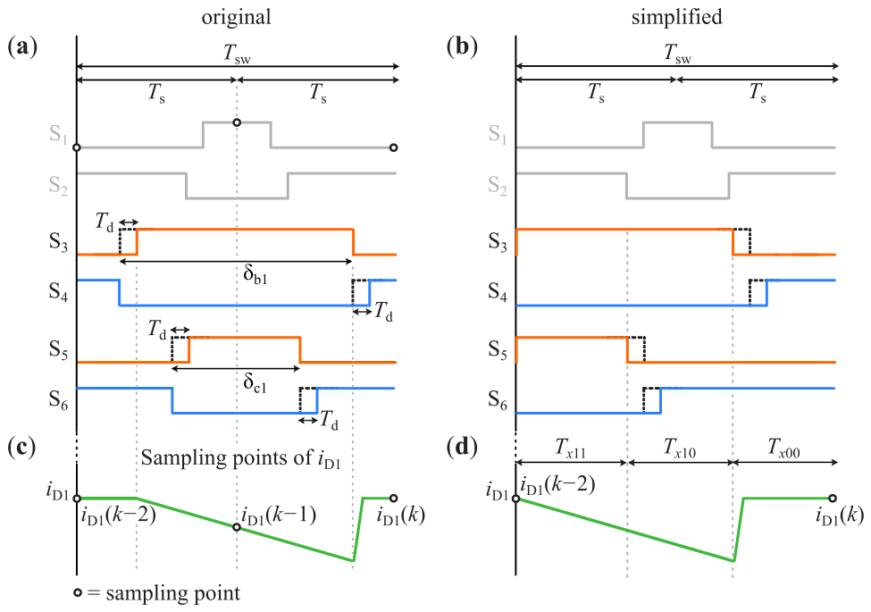
In Section 3, the conduction conditions of the FDC were defined according to the PFVVs. The conducting interval of each voltage vector, i.e., their SVPWM switching state can be calculated from the duty cycles of the other two healthy phases in the faulted power inverter (Figure 6a). Given that the open-phase fault is located in phase a 1 , the conduction interval is based on the duty cycles of phases b 1 and c 1 , denoted as δ b 1 and δ c 1 , respectively.
The conducting intervals of PFVVs v x 00 and v x 11 are denoted as T x 00 and T x 11 , respectively, and they are calculated as
T x 00 = 1 max δ b 1 , δ c 1 · T s + T d
T x 11 = min δ b 1 , δ c 1 · T s T d ,
where T s is the sampling period and T d is the dead time of the power switches. Hence, the dead time allocates more conduction time for D 2 , and shortens the conduction time for D 1 , but in a real machine drive, the difference is negligible.
The conducting intervals for v x 10 and v x 01 , T x 10 and T x 01 , respectively, can be defined as one, as the conduction conditions for these PFVVs are the same.
T x 10 = T x 01 = max δ b 1 , δ c 1 min δ b 1 , δ c 1 · T s
The dead time T d does not alter T x 10 or T x 01 , since the PFVVs mutually compensate for the resulting conducting interval error within each switching period T sw . In Figure 6a, if the conducting interval of one vector is reduced due to T d , the duration of the adjacent vector is correspondingly increased. Consequently, the net conducting interval over one switching period remains unaffected by the dead time.

4.2. Initial Condition

The initial condition I 0 in Equations (9) and (11) is the value of the FDC at the beginning of the current sampling step, where k denotes the discrete-time index of the current sampling instant. The value of initial condition depends on the conduction interval, which is determined by the currently conductive PFVV. In practical implementation, two cases must be distinguished: the initialization of I 0 at the instant when the open-phase fault occurs and its update during the subsequent sampling steps.
The initialization rule for I 0 is based on the last available current sample before the fault. Since the FDC is defined as the phase current of the faulted phase, i D = i a 1 , and the phase currents are continuously sampled for current control, I 0 is initialized from the last sampled value of i a 1 . In the following sampling steps, the initial condition within each sampling interval is described below using a simplified representation of the SVPWM switching sequence.
For analytical simplicity, we assume that the SVPWM switching states are not symmetrically distributed within the switching period, as it is seen in Figure 6a. Instead, we simplify the sequence by assuming that in the case of i D 1 (Figure 6b), v x 11 is applied first, followed by the vectors v x 10 or v x 01 . This rearrangement of the PWM states does not alter the initial or final values of i D 1 within the given switching interval, since the duty cycles remain unchanged and only their temporal positions within the switching period are modified (Figure 6d). In the case of i D 2 , PFVV v x 00 is applied first.
First, let us consider the conduction of i D 1 . When E a 1 + M is between 0 V and 2 v D / 3 (Equation (18)), no conduction path exists; therefore, i D 1 cannot flow. When E a 1 + M is between 2 v D / 3 and V dc + 2 v D / 3 (Equation (22)), i D 1 is conducted only during the interval of v x 11 . In this case, the initial condition corresponds to the FDC value from the previous sampling interval. When E a 1 + M exceeds V dc + 2 v D / 3 , i D 1 flows both when v x 11 is active and when PFVVs v x 10 or v x 01 are active. Because of the rearrangement of the SVPWM sequences (Figure 6c,d), the initial condition for v x 11 remains equal to the FDC value from the previous sampling interval. For v x 10 or v x 01 , however, the initial condition corresponds to the i D 1 resulting from the previously applied vector v x 11 within the same sampling interval. The resulting current value is the amplitude of i D 1 in this sampling interval.
Accordingly, within a single sampling interval, i D 1 is first calculated for v x 11 , considering that in this case v PN = 0 (Equation (30)). It is then calculated for v x 10 or v x 01 , where v PN = V dc / 3 (Equation (31)). The result of this calculation is the final value of i D 1 in this interval.
An analogous reasoning can be applied to the case of i D 2 . In this case, the conduction intervals depend on the negative sum E a 1 + M (Equations (24) and (29)). Consequently, v x 00 is activated first, for which v ON = 0 (Equation (32)) is assumed. It is followed by v x 10 or v x 01 , for which v ON = V dc / 3 (Equation (33)) applies.

4.2.1. Compensation of the Sampling-Induced Error in i D

In conventional double-sampling methods, signals are sampled twice within one switching period, typically at the beginning and at the midpoint of the interval (Figure 6c). This sampling approach offers two primary advantages: it is easy to implement in the microcontroller unit (MCU), and it captures the average value of the current ripple, thereby improving current control accuracy [17].
However, when sampling the FDC, this approach introduces a sampling-induced error due to the conduction characteristics of the FDC. The current i D flows only during conducting PFVVs and approximately varies linearly during the conduction interval (Figure 6c), increasing or decreasing depending on the polarity of the current. As a result, when the sampling instant occurs at the midpoint of the switching interval, the sampled value i D ( k 1 ) corresponds to the average FDC over the conduction interval rather than its peak value (Figure 6c).
Consequently, the sampled value underestimates the initial current I 0 ( k ) required for the FDC calculations in Equations (9) and (11). To compensate for this sampling-induced error, the initial current is estimated from two previously sampled values of the FDC. The compensation of the sampling-induced error depends on which of the freewheeling diodes is conducting. For i D 1 , the initial current is
I 0 , D 1 ( k ) = i D ( k 1 ) + min 0 ,   i D ( k 1 ) i D ( k 2 ) .
For i D 2 , the initial current is
I 0 , D 2 ( k ) = i D ( k 1 ) + max 0 ,   i D ( k 1 ) + i D ( k 2 ) .
The correction term in Equations (37) and (38) can be interpreted as a slope-limited extrapolation of the FDC based on two consecutive samples. The difference between i D ( k 1 ) and i D ( k 2 ) provides an estimate of the current slope, which is used to approximate the peak value of the current within the switching interval. The use of the max ( · ) and min ( · ) operators constrains the extrapolation to physically consistent current evolution. The zero value in the operators ensures that no correction is applied when the previously sampled FDC is zero. In this case, the average value of the conduction interval is also zero, which implies that the corresponding peak current is zero as well. Therefore, no compensation of the sampled value is required.

4.2.2. Conduction Mode Dependent Behavior

The sampling-error compensation is primarily required in discontinuous conduction mode (DCM), where the FDC reaches zero within each switching period. In DCM, conventional double sampling introduces a significant error, since the sampled value represents the average current over the conduction interval and therefore underestimates the initial current required by the analytical model (Figure 6c). The proposed compensation method assumes that the current slope d i D / d t remains approximately constant between consecutive switching periods. This assumption is justified by the relatively large electrical time constant L s / R s compared with the switching period T sw and is generally valid in DCM, where the current returns to zero within each switching cycle and evolves from similar initial conditions.
In contrast, in continuous conduction mode (CCM), the current does not reach zero and the slope d i D / d t can vary more significantly from one switching period to another due to the continuous evolution of the system states, as depicted in Figure 5, where the right enlarged window of the simulated FDC illustrates the transition from DCM to CCM. The analytical threshold for DCM–CCM transition is derived in Appendix A. As a result of the continuous conduction, the underlying assumption of the compensation method is no longer strictly valid, and the method can no longer accurately compensate for the sampling-induced error.
However, in CCM, the conventional sampling introduces only a minor error, as the sampled current corresponds to the average of a relatively smooth waveform without discontinuities. Consequently, the impact of sampling error on the analytical calculation is limited. Nevertheless, the proposed sampling-error compensation is retained in this operating regime to maintain methodological consistency across all operating conditions, although its effect on the final result is negligible.

4.3. Experimental and Simulation Framework

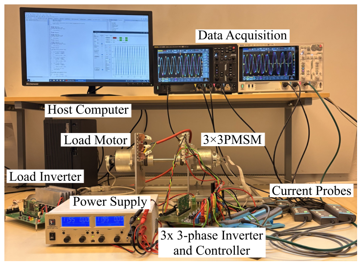
The proposed analytical method is validated using experimental measurements obtained from a real motor drive system shown in Figure 7. The setup consists of a 3 × 3PMSM supplied by a power source via three two-level three-phase inverters and controlled by a Texas Instruments F28377 digital signal processor-based microcontroller (MCU). During experimental validation, the relevant signals were sampled by the MCU at a sampling frequency of f s = 40   kHz . Without loss of generality, the open-phase fault was emulated by disabling the gate signals of the inverter leg of phase a 1 using the digital signal processor trip-zone module, while the freewheeling diodes remained operational. The MOSFET modules used are Texas Instruments CSD19533KCS. Under these conditions, the FDC is measured with a Rigol HDO1074 oscilloscope using a Micsig CP2100 current probe for defined operating points, which include both the constant-torque and FW regions and are summarized in Table 2. The parameters of the employed motor drive are shown in Table 3. The maximum speed the 3 × 3PMSM can reach is 3000   rpm . The control scheme is based on PI controllers, field-oriented control (FOC), and SVPWM. Detailed average-difference current regulation of the 3 × 3PMSM is described in [29,31].
The simulation model of the 3 × 3PMSM drive is implemented in a MATLAB/Simulink R2025b environment and consists of three main components: the 3 × 3PMSM model, the triple two-level three-phase power inverter model, and the control block. The 3 × 3PMSM is modeled using the phase-domain voltage model, which enables direct representation of the phase quantities under open-phase fault conditions. The inverter is modeled in the Simscape physical domain using predefined power-electronic components to closely reproduce the experimental hardware, while the control block emulates the MCU by executing the control algorithm at the sampling frequency f s .
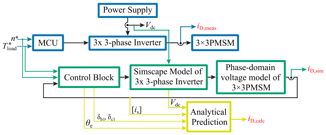
To replicate the measured operating conditions, the simulation inputs are derived from the experimental setup, as shown in Figure 8. These include the reference mechanical speed and load torque. In addition, the V dc is measured during the experiment and used as an input to the simulation model to better reflect the real drive conditions. The simulated FDC is obtained directly from the motor model, which emulates the current-sensing behavior of the real 3 × 3PMSM drive. Consequently, the simulated FDC contains switching-frequency oscillations, similarly to the measured FDC.
The analytical FDC prediction is computed within the control block, reflecting its intended MCU implementation. Its inputs are obtained from the simulation model and consist of the basic quantities from which all variables required for the FDC calculation are derived, as shown in Figure 8. The conduction conditions, post-conduction values of v PN and v ON , and initial-current definitions derived in the preceding sections provide the complete set of inputs required to evaluate Equations (9) and (11) over each sampling interval. For clarity, the resulting conduction states and the corresponding parameters used in the analytical calculation are summarized in Table 4. Since the analytical FDC is evaluated at discrete control sampling instants, it is updated only twice per switching period and does not capture instantaneous discontinuous switching behavior within each cycle. Instead, it represents the averaged envelope of the FDC, and the evaluation of the analytical prediction is therefore based on the outer envelopes of the measured, simulated, and calculated signals.
From an implementation point of view, the proposed analytical FDC prediction can be integrated into the existing machine drive control algorithm with minimal additional computational effort, since the FDC is obtained directly from explicit analytical equations and algebraic conduction conditions within each sampling interval. The required inputs, such as the sampled phase currents, duty cycles, DC-link voltage, and rotor position, are already available in the control algorithm, as illustrated in Figure 8. Therefore, the method does not require finite-element calculations, magnetic lookup tables, or additional current sampling synchronized with the switching states. This is an advantage compared with previous approaches, where an additional switching-state-synchronized sampling method was introduced specifically for FDC measurement [17].

5. Results

Based on the experimental and simulation framework established in the previous section, this section presents the validation results for the proposed analytical prediction of the FDC. First, the measured phase currents before and during an open-phase fault are presented to illustrate the effect of the fault on the 3 × 3PMSM drive. Next, the influence of speed and load on the FDC is analyzed. Finally, the analytical prediction is evaluated through a comparative error analysis with respect to both simulated and measured FDC envelopes.

5.1. Measured Phase Currents During Open-Phase Fault

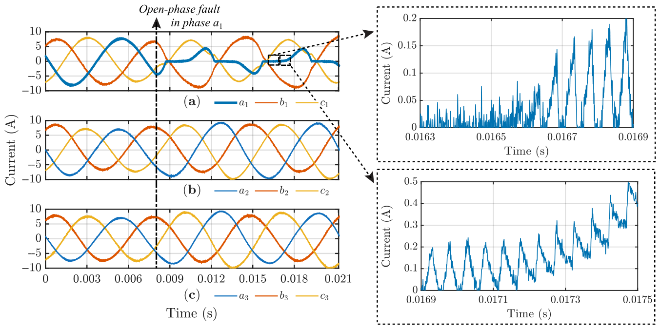
Figure 9 shows the measured phase currents of the three winding sets before and after the application of the open-phase fault in phase a 1 in the FW region. The three subplots in Figure 9 (left), labeled (a)–(c), correspond to winding sets 1, 2, and 3, respectively. The vertical dash-dotted line marks the instant at which the open-phase fault is applied in phase a 1 . After the fault, the current in the faulted phase, hereafter referred to as the freewheeling diode current, deviates significantly from a sinusoidal waveform. Consequently, the currents in the two healthy phases of the affected winding set also become distorted, whereas the currents in the remaining two healthy winding sets retain their sinusoidal shape. In addition, the amplitudes of the healthy phase currents increase after the fault, since they must compensate for the reduced torque contribution of the faulted phase while preserving the pre-fault reference speed and load torque.
The right-hand insets in Figure 9 provide enlarged views of the faulted-phase current, i.e., the FDC. The top right-hand inset shows the beginning of FDC conduction. The bottom right-hand inset shows the subsequent FDC evolution, where both DCM, characterized by intervals in which the current falls to zero, and CCM, characterized by nonzero current throughout the switching period, can be observed. The analytical threshold for DCM–CCM transition is derived in Appendix A.

5.2. Influence of Speed and Load on Freewheeling Diode Current

Representative operating points were selected to cover the constant-torque region, base speed, and the FW region under both no-load and loaded conditions, in order to assess the accuracy of the proposed FDC prediction method across the full operating range.
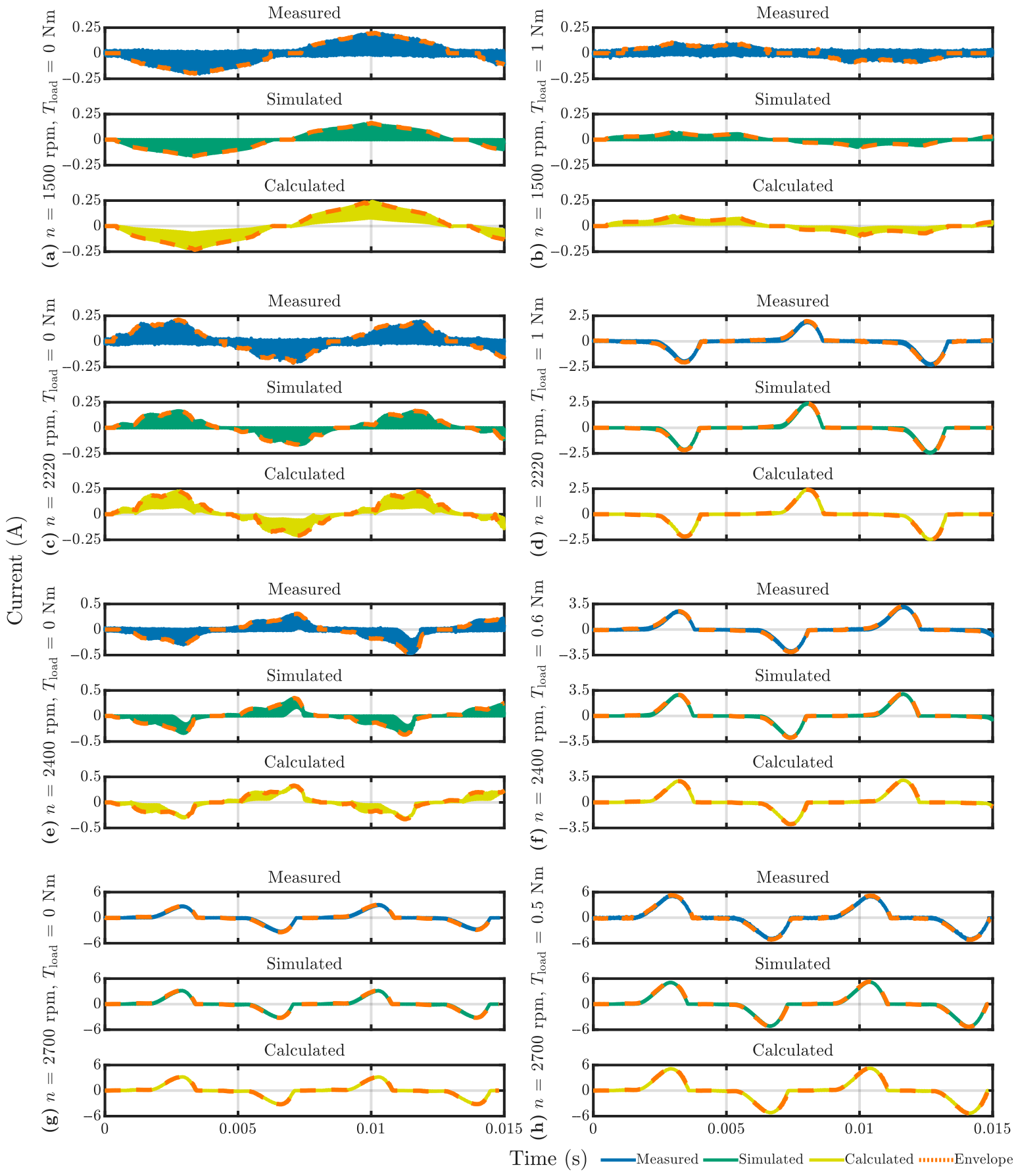
Figure 10 presents the measured, simulated, and analytically predicted (calculated) FDCs together with their corresponding envelopes for representative operating points at different mechanical speeds and load torques. The considered speeds are n = 1500   rpm , corresponding to operation in the constant-torque region (Figure 10a,b), n = 2220   rpm at base speed (Figure 10c,d), n = 2400   rpm at the onset of FW (Figure 10e,f), and n = 2700   rpm deep in the FW region (Figure 10g,h).
At n = 1500   rpm , the FDC is relatively small and exhibits a discrete waveform, indicating discontinuous conduction (Figure 10a,b). At base speed and at the beginning of FW, i.e., n = 2220   rpm and n = 2400   rpm , increasing the load torque results in a transition toward predominantly continuous conduction, where the FDC no longer reaches zero within a switching period. Moreover, the current amplitude increases significantly. Under no-load conditions (Figure 10c,e), the FDC amplitude is of the order of 0.1   A , whereas at maximum load it increases to the order of 1   A (Figure 10d,f). At n = 2700   rpm , corresponding to deep FW operation, the FDC remains comparatively large even at no load (Figure 10g). This is due to the increased stator current required to establish the FW condition.
Figure 10 confirms that both the conduction mode and the amplitude of the FDC are strongly influenced by the operating speed and load torque, while also demonstrating good agreement among the measured, simulated, and analytically predicted results.

5.3. Comparative Error Analysis of the Analytical Prediction

To comprehensively assess the accuracy of the analytical FDC prediction, both absolute and relative error metrics are considered. The absolute error quantifies the deviation with respect to a fixed base value, whereas the relative error relates the deviation to the corresponding signal metric.
First, an absolute current-normalized error measure is introduced. In this formulation, the normalization is performed with respect to the maximum current, I max = 16.6   A . The absolute RMS and peak errors are therefore defined as
e RMS , abs = I RMS , calc I RMS , ref I max ,
e peak , abs = I peak , calc I peak , ref I max ,
where the reference signal is either simulated or measured FDC. Consequently, the absolute current composite error is defined as the root-sum-squared of the RMS and peak-value errors
e RSS , abs = e RMS , abs 2 + e peak , abs 2 .
This metric captures both the average RMS deviation and the maximum amplitude deviation, distinguishing operating points where both errors are moderate from those where one contribution dominates. The absolute error metrics express the deviation of the analytically predicted signal from the measured or simulated signal with respect to the global current scale of the machine drive, which makes them suitable for comparing operating points with substantially different current amplitudes.
In addition, a relative root-sum-squared error e RSS , rel is considered. It is composed of the relative RMS-current error and relative peak-current error.
e RSS , rel = e RMS , rel 2 + e peak , rel 2 ,
where
e RMS , rel = I RMS , calc I RMS , ref I RMS , ref ,
e peak , rel = I peak , calc I peak , ref I peak , ref .
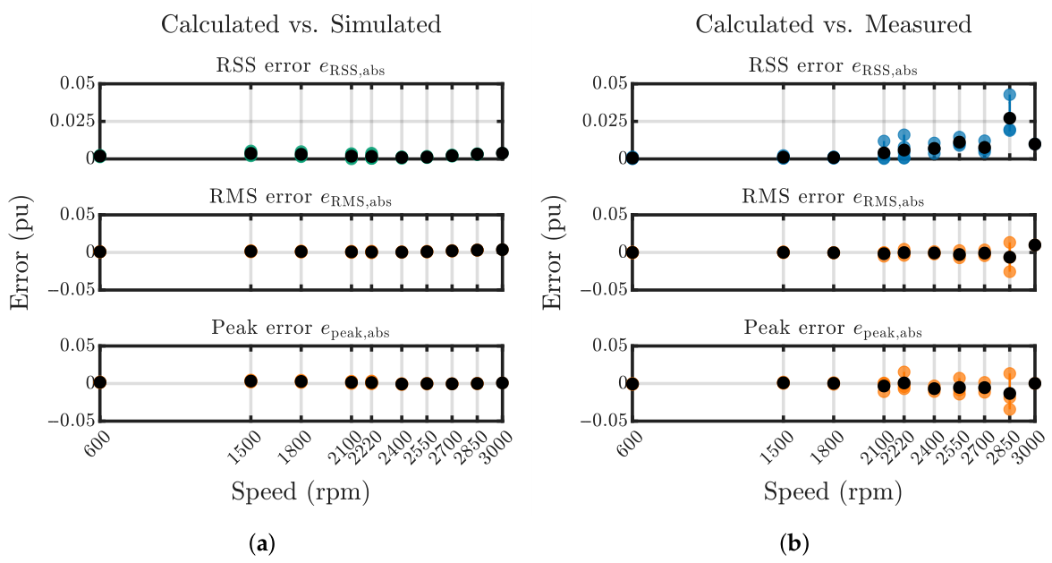
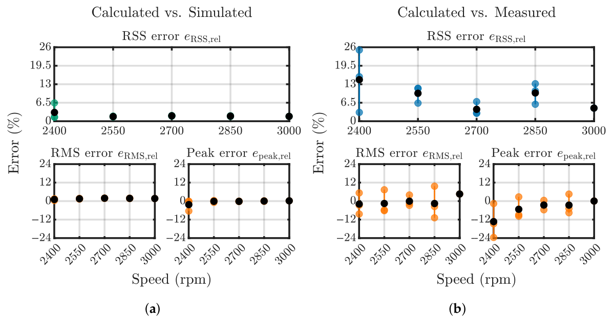
The error metrics for operating points from Table 2 are depicted in Figure 11 and Figure 12 which summarize the absolute and relative error metrics of the analytically predicted current envelopes with respect to the simulated and measured FDC envelopes. In all figures, the black marker denotes the mean value of the error at a given speed, whereas the colored markers represent individual operating points and illustrate the deviation from the mean error.
In Figure 11a, the absolute error results show that the agreement between the analytical and simulated signals is very good over the entire investigated speed range, since the absolute RSS, RMS, and peak errors remain clustered close to zero for all operating points. In particular, e RSS , abs with respect to the simulated signal remains only a few 0.001   pu , while the absolute RMS and peak errors also stay close to zero without any pronounced speed- or load-dependent trend.
In contrast, the absolute errors with respect to the measured signal (Figure 11b) are more dispersed, especially at higher speeds, which can be attributed to the increased current levels at these operating points, leading to larger absolute error values. Overall, these results indicate that the analytical model reproduces the simulated signal with high accuracy, whereas the discrepancy with the measured signal is larger, which is expected due to measurement uncertainty and additional non-ideal effects not captured by the analytical formulation.
A similar trend is observed in the relative error evaluation (Figure 12); however, the relative error is presented only for the FW region. In the constant-torque region, the absolute FDC values are near zero (e.g., range of 0.1 A under no-load). Dividing by these near-zero reference values artificially inflates the relative error percentage, masking the actual agreement. Therefore, absolute error metrics (Figure 11) provide a more physically meaningful evaluation in this region.
With respect to the simulated signal, e RSS , rel , e RMS , rel and e peak , rel remain low throughout the considered FW region, staying within only a few percent. This confirms that the analytical prediction captures not only the current amplitudes but also the envelope shape of the simulated signal with good fidelity.
By comparison, the relative errors with respect to the measured signal (Figure 12b) are clearly higher and exhibit a larger scatter. The relative RSS error e RSS , rel is highest at the lower end of the investigated FW region and decreases toward higher speeds. The reason is that, at no-load or low-load operating points, the FDC amplitude is still in the 0.1   A range, such that even minor absolute deviations lead to comparatively large relative errors. This is confirmed by Figure 11b, which shows that the corresponding absolute errors in the lower FW region remain very small. In contrast, e RMS , rel and e peak , rel remain mainly centered near zero, albeit with a broader spread.
Table 5 quantitatively summarizes the error metrics for the representative operating points whose measured and simulated waveforms are shown in Figure 10. The results show good agreement between the analytically predicted FDC envelope values and both the simulated and measured results across the tested speed and load range. For the calculated-versus-simulated comparison, the absolute RMS error e RMS , abs remains in the range of 0.040 × 10 3 to 2.697 × 10 3 pu, while the peak absolute error e peak , abs remains below 4.736 × 10 3 pu. The calculated-versus-measured comparison shows similarly small absolute RMS errors e RMS , abs , with absolute values between 0.0551 × 10 3 and 4.333 × 10 3 pu. Some relative errors e RMS , rel , e peak , rel are comparatively larger in the constant-torque region, where the absolute FDC values are close to zero. As it was stated before, dividing by these near-zero reference values artificially inflates the relative error percentage. Overall, the error values in Table 5 support the visual agreement observed in Figure 10 and confirm the validity of the proposed analytical calculation across the representative operating conditions.
Taken together, the two figures and Table 5 show that the proposed analytical model is highly consistent with the simulated results and remains in reasonable agreement with the measurements, although the latter naturally exhibit larger deviations due to experimental variability and unmodeled parasitic effects.

6. Discussion

6.1. Main Findings and Validation

This paper presented an analytical method for real-time prediction of the FDC under an inverter open-phase fault in a weakly magnetically coupled triple three-phase surface-mounted permanent magnet synchronous machine drive. Starting from the phase-domain voltage equations, the FDC conduction paths were analyzed for both freewheeling diodes, and analytical expressions were derived for the corresponding FDCs. In addition, switching-state-dependent conduction conditions were established using PFVVs. To improve applicability in practical digital control systems, a compensation method for the sampling-induced error was also introduced through correction of the initial condition of the FDC differential equation.
The proposed method was validated using both experimental measurements and a detailed simulation model over a broad operating range covering the constant-torque region, base-speed operation, and the FW region. The comparison of measured, simulated, and analytically predicted FDC waveforms showed that the analytical model accurately captures the main conduction characteristics of the FDC, including its envelope, the transition from discontinuous to continuous conduction mode, and the conduction-boundary-related waveform features within one electrical period. In particular, the analytical prediction was shown to replicate the simulated current with very high accuracy over the full investigated speed range and to remain in reasonable agreement with the measured current despite the presence of measurement uncertainty and unmodeled parasitic effects.
The quantitative error analysis further confirmed the validity of the proposed approach. The absolute error metrics remained small over the entire operating range, while the relative error analysis in the FW region showed that the analytical prediction accurately reproduces not only the FDC amplitudes but also the envelope shape. The larger deviations observed with respect to the measured signals were mainly associated with low-current operating points, where even small absolute discrepancies lead to comparatively large relative errors, and with high-speed experimental conditions, where practical non-idealities become more pronounced.

6.2. Scalability and Limitation of the Analytical Framework

Although the experimental validation in this work was performed on a low-voltage and low-power drive, the proposed analytical model is not inherently limited to this power range. In fact, the present setup represents a conservative case with respect to the influence of the diode forward voltage, since V dc = 12   V and v D = 0.9   V , giving a comparatively high ratio of v D / V dc = 0.075 . Therefore, variations in v D have a more pronounced influence on the diode conduction conditions and the resulting FDC amplitude. In high-voltage drives, such as 400 V or 800 V traction applications, this ratio becomes much smaller, and the diode forward voltage is expected to have a significantly lower influence on the predicted FDC envelope. Thus, when appropriate device parameters are used, the analytical model is expected to remain applicable to higher-voltage and higher-power drive systems.
At the same time, the proposed analytical framework was derived for a three-phase two-level power inverter. Therefore, direct application to other inverter topologies would require a topology-specific derivation. For example, in multilevel inverters, the number of possible post-fault voltage vectors is larger than in two-level inverters. In addition, the FDC paths may differ depending on the selected topology, since the faulted phase may have conduction paths not only toward the positive and negative DC-link terminals, but also involving the neutral point. Consequently, the inverter-side voltage terms, the conduction conditions related to the PFVV switching states, and the corresponding conduction intervals would need to be derived again for the selected multilevel topology.
A further limitation is that the analytical expressions were derived for a weakly magnetically coupled triple three-phase surface-mounted PMSM. Extension to other machine types or winding configurations is possible in principle, but the phase-domain voltage equations and coupling terms would need to be adapted to the considered machine. Moreover, while the proposed method demonstrates good performance for the considered surface-mounted PMSM, its reliance on a constant inductance matrix limits its direct application to interior PMSMs and other machines with pronounced magnetic saturation. For such machines, the current-dependent nature of the stator inductance would need to be included in order to capture saturation and cross-saturation effects [26,27,28]. Therefore, the general methodology can be transferred to other machine and inverter configurations, but the final analytical expressions are topology- and machine-dependent.

6.3. Implications for Post-Fault Control and Future Work

Overall, the results demonstrate that the proposed analytical method provides an accurate and computationally efficient prediction of the FDC under open-phase fault conditions in both the constant-torque and FW regions. In multiphase drives, this prediction is important for post-fault control because the current flowing through the freewheeling diodes must be considered to regulate the drive after the fault. By accounting for the FDC, continuous operation can be maintained with equal or reduced performance, which is generally not feasible in conventional three-phase drives due to the lack of phase redundancy.
In addition, the proposed FDC prediction can be used as the basis for an online thermal protection or post-fault current limiting scheme. Since the analytical model predicts the FDC in real time, the predicted FDC amplitude can be monitored and compared with a predefined allowable limit determined by the thermal capability of the power inverter and freewheeling diodes. For example, by estimating the expected diode power dissipation, the controller can evaluate the associated thermal stress and estimate the junction temperature [32]. If the predicted FDC remains below the allowable limit, the machine drive can continue operating in post-fault mode. If the predicted value exceeds the limit, the controller can reduce the post-fault current or torque reference to lower the FDC and the corresponding thermal stress. If the predicted stress remains excessive even after derating, the protection scheme can safely shut down the drive.
Future work will focus on real-time implementation of the proposed method and on FDC-based compensation strategies for improved post-fault performance. In addition, future research should address the extending of the modeling framework to include current-dependent inductance or flux-linkage maps for machines where saturation effects cannot be neglected.

Author Contributions

Conceptualization, Ž.S. and K.D.; methodology, Ž.S.; software, Ž.S. and M.N.; validation, Ž.S., H.L. and K.D.; formal analysis, Ž.S.; investigation, Ž.S.; resources, M.N., H.L. and K.D.; data curation, Ž.S. and M.N.; writing—original draft preparation, Ž.S.; writing—review and editing, Ž.S., H.L., M.N. and K.D.; visualization, Ž.S., K.D. and H.L.; supervision, M.N., H.L. and K.D.; project administration, K.D.; funding acquisition, K.D. All authors have read and agreed to the published version of the manuscript.

Funding

This work was funded by the Slovenian Research and Innovation Agency (ARIS) through research core funding No. P2-0258.

Institutional Review Board Statement

Not applicable.

Informed Consent Statement

Not applicable.

Data Availability Statement

The raw data supporting the conclusions of this article will be made available by the corresponding author on request.

Conflicts of Interest

The authors declare no conflicts of interest.

Abbreviations

The following abbreviations are used in this manuscript (in alphabetical order):
CCMContinuous conduction mode
DCMDiscontinuous conduction mode
FDCFreewheeling diode current
FWField-weakening
MCUMicrocontroller unit
PFVVPost-fault voltage vector
PMSM      Permanent magnet synchronous machine
PWMPulse width modulation
SVPWMSpace vector pulse width modulation
3 × 3PMSMTriple three-phase surface-mounted permanent magnet synchronous machine

Appendix A. DCM–CCM Boundary Condition

This appendix derives the analytical condition for the transition between the discontinuous conduction mode (DCM) and continuous conduction mode (CCM) of the FDC. The derivation is shown for diode D 2 , since this diode determines the current behavior and the onset of continuous conduction observed in Figure 9 (bottom right).

Appendix A.1. Voltage Condition During D2 Conduction

During conduction of diode D 2 (Figure 2b), the voltage equation of the faulted phase a 1 can be written as
L s d i D 2 d t + R s i D 2 = v D + v ON E a 1 + M .
For an isolated-neutral three-phase winding set, the conduction of one freewheeling diode shifts the neutral point potential. In particular, a diode voltage drop v D applied to one phase shifts the neutral point by v D / 3 , while 2 v D / 3 of the diode drop appears in the faulted phase-to-neutral voltage v AN . When diode D 2 conducts, the terminal voltage of the faulted phase is clamped to the negative DC link through the diode, i.e.,
v AO = v D .
If m healthy phases are connected to the positive DC link ( V dc ), where m 0 , 1 , 2 , the neutral point voltage with respect to the negative DC rail becomes
v NO = v ON = m V dc v D 3 .
Consequently, the phase-to-neutral voltage of the faulted phase is
v AN = v D + v ON = v D m V dc v D 3 = m V dc + 2 v D 3 .
Within a single switching period T sw , the healthy phases are modulated using SVPWM, dividing the period into sub-intervals corresponding to the PFVVs. Let T x 00 , T x 01 / 10 (where T x 01 / 10 = T x 01 + T x 10 ), and T x 11 be the durations when m = 0 , m = 1 , and m = 2 healthy phases are connected to the positive DC link, respectively. The resulting phase-to-neutral voltages v AN for each interval are
v AN , x 00 = 2 v D 3 , for m = 0 ,
v AN , x 01 / 10 = V dc + 2 v D 3 , for m = 1 ,
v AN , x 11 = 2 V dc + 2 v D 3 , for m = 2 .

Appendix A.2. Volt-Second Balance at the DCM–CCM Boundary for D2

The DCM–CCM boundary is reached when the diode current decreases to zero exactly at the end of the switching period. In this case,
i D 2 ( T sw ) = 0 ,
and the transition condition can be obtained from the inductive volt-second balance over one switching period,
0 T sw v AN E a 1 + M d t = 0 .
By splitting the integral according to the PFVV durations, the following condition is obtained:
0 = E a 1 + M 2 v D 3 T x 00 + E a 1 + M V dc + 2 v D 3 T x 01 + T x 10 + E a 1 + M 2 V dc + v D 3 T x 11 .
Since
T x 00 + T x 01 + T x 10 + T x 11 = T sw ,
the previous expression can be simplified to
E a 1 + M T sw 2 v D 3 T sw V dc 3 T x 01 + T x 10 + 2 T x 11 = 0 .
Dividing by T sw and isolating the back-EMF and mutual coupling term ( E a 1 + M ) crit provides the transition boundary
E a 1 + M crit = 2 v D 3 V dc 3 T sw T x 01 + T x 10 + 2 T x 11 .
The term V dc 3 T sw T x 01 + T x 10 + 2 T x 11 represents the average positive potential established at the neutral point by the PWM switching of the healthy phases.

Appendix A.3. DCM–CCM Transition Criterion for D2

To transition from DCM to CCM, the induced voltage in the faulted phase ( E a 1 + M ) must be sufficiently negative to overcome both the static forward voltage drop of the diode barrier ( 2 v D / 3 ) and this average dynamic neutral point bias.
The conduction modes are thus defined as
  • DCM Operation: ( E a 1 + M ) > ( E a 1 + M ) crit . The net volt-seconds are negative, forcing the current to decay to zero before the end of the period.
  • CCM Operation: ( E a 1 + M ) < ( E a 1 + M ) crit . The net volt-seconds are positive, preventing the current from returning to zero and resulting in a continuous accumulation of freewheeling diode current.
While the sum T x 01 + T x 10 + 2 T x 11 is constant during any single switching period T sw , it varies continuously throughout the fundamental electrical period according to the sinusoidal modulated duty cycles of the healthy phases. Consequently, the boundary condition establishes a dynamically moving threshold. The best case for immunity against unwanted freewheeling diode current (maintaining DCM) occurs when PFVV v x 11 dominates the switching period, as it maximizes the opposing potential barrier. Conversely, PFVV v x 00 provides no counter-EMF and present the worst-case scenario.

References

  1. Slunjski, M. Control of a Nine-Phase Symmetrical PMSM with Reduced Rare Earth Material. Ph.D. Thesis, Liverpool John Moores University, Liverpool, UK, 2020. [Google Scholar]
  2. Rubino, S.; Bojoi, I.R.; Mandrile, F.; Armando, E. Modular Stator Flux and Torque Control of Multi-Three-Phase Induction Motor Drives. IEEE Trans. Ind. Appl. 2020, 56, 6507–6525. [Google Scholar] [CrossRef]
  3. Son, D.K.; Kwon, S.H.; Kim, D.O.; Song, H.S.; Lee, G.H. Control Comparison for the Coordinate Transformation of an Asymmetric Dual Three Phase Synchronous Motor in Healthy and Single-Phase Open Fault States. Energies 2021, 14, 1735. [Google Scholar] [CrossRef]
  4. Petrun, M.; Černelič, J. Sensitivity analysis of MTPA control to angle errors for synchronous reluctance machines. Mathematics 2025, 13, 23. [Google Scholar] [CrossRef]
  5. Hu, Y.; Zhu, Z.Q.; Odavic, M. Comparison of Two-Individual Current Control and Vector Space Decomposition Control for Dual Three-Phase PMSM. IEEE Trans. Ind. Appl. 2017, 53, 4483–4492. [Google Scholar] [CrossRef]
  6. Rubino, S.; Dordevic, O.; Bojoi, R.; Levi, E. Modular Vector Control of Multi-Three-Phase Permanent Magnet Synchronous Motors. IEEE Trans. Ind. Electron. 2021, 68, 9136–9147. [Google Scholar] [CrossRef]
  7. Rubino, S.; Mandrile, F.; Armando, E.; Bojoi, I.R.; Zarri, L. Fault-Tolerant Torque Controller Based on Adaptive Decoupled Multi-Stator Modeling for Multi-Three-Phase Induction Motor Drives. IEEE Trans. Ind. Appl. 2022, 58, 7318–7335. [Google Scholar] [CrossRef]
  8. Gholamian, M.; Beik, O.; Arshad, M. A Review of State-of-the-Art Multiphase and Hybrid Electric Machines. Electronics 2024, 13, 3636. [Google Scholar] [CrossRef]
  9. Sui, Y.; Zheng, P.; Wu, F.; Yu, B.; Wang, P.; Zhang, J. Research on a 20-Slot/22-Pole Five-Phase Fault-Tolerant PMSM Used for Four-Wheel-Drive Electric Vehicles. Energies 2014, 7, 1265–1287. [Google Scholar] [CrossRef]
  10. Frikha, M.; Croonen, J.; Deepak, K.; Benômar, Y.; El Baghdadi, M.; Hegazy, O. Multiphase Motors and Drive Systems for Electric Vehicle Powertrains: State of the Art Analysis and Future Trends. Energies 2023, 16, 768. [Google Scholar] [CrossRef]
  11. Cui, S.; Zhao, T.; Du, B.; Cheng, Y. Multiphase PMSM with Asymmetric Windings for Electric Drive. Energies 2020, 13, 3765. [Google Scholar] [CrossRef]
  12. Scuiller, F.; Charpentier, J.F.; Semail, E. Multi-star multi-phase winding for a high power naval propulsion machine with low ripple torques and high fault tolerant ability. In Proceedings of the 2010 IEEE Vehicle Power and Propulsion Conference, Lille, France, 1–3 September 2010; pp. 1–5. [Google Scholar] [CrossRef]
  13. Hasoun, M.; Afia, A.E.; Chikh, K.; Khafallah, M.; Benkirane, K. A PWM strategy for dual three-phase PMSM using 12-sector vector space decomposition for electric ship propulsion. In Proceedings of the 2018 19th IEEE Mediterranean Electrotechnical Conference (MELECON), Marrakech, Morocco, 2–7 May 2018; pp. 243–248. [Google Scholar] [CrossRef]
  14. Bouyahia, O.; Betin, F.; Yazidi, A. Fault-Tolerant Fuzzy Logic Control of a 6-Phase Axial Flux Permanent-Magnet Synchronous Generator. Energies 2022, 15, 1301. [Google Scholar] [CrossRef]
  15. Zabaleta, M.; Jones, M.; Levi, E. A tuning procedure for the current regulator loops in multiple three-phase permanent magnet machines with low switching to fundamental frequency ratio. In Proceedings of the 2017 19th European Conference on Power Electronics and Applications (EPE’17 ECCE Europe), Warsaw, Poland, 11–14 September 2017; pp. 1–10. [Google Scholar] [CrossRef]
  16. Zoric, I.; Jones, M.; Levi, E. Arbitrary Power Sharing Among Three-Phase Winding Sets of Multiphase Machines. IEEE Trans. Ind. Electron. 2018, 65, 1128–1139. [Google Scholar] [CrossRef]
  17. Zhang, Z.; Hu, Y.; Lee, C.H.T.; Luo, G.; Gong, C.; Alkahtani, M. Diagnosis of Free-Wheeling Diodes in PMSM Drives Based on Residual Current Under Open-Circuit Faults. IEEE Trans. Ind. Electron. 2025, 72, 3269–3279. [Google Scholar] [CrossRef]
  18. Orlowska-Kowalska, T.; Wolkiewicz, M.; Pietrzak, P.; Skowron, M.; Ewert, P.; Tarchala, G.; Krzysztofiak, M.; Kowalski, C.T. Fault Diagnosis and Fault-Tolerant Control of PMSM Drives–State of the Art and Future Challenges. IEEE Access 2022, 10, 59979–60024. [Google Scholar] [CrossRef]
  19. Wang, B. Multiple 3-Phase Fault Tolerant Permanent Magnet Machine Drives: Design and Control, 1st ed.; John Wiley & Sons, Incorporated: Newark, NJ, USA, 2025. [Google Scholar]
  20. Jahns, T.; Caliskan, V. Uncontrolled generator operation of interior PM synchronous machines following high-speed inverter shutdown. IEEE Trans. Ind. Appl. 1999, 35, 1347–1357. [Google Scholar] [CrossRef]
  21. Gong, C.; Hu, Y.; Gan, C.; Chen, G.; Alkahtani, M. Modeling, Analysis, and Attenuation of Uncontrolled Generation for IPMSM-Based Electric Vehicles in Emergency. IEEE Trans. Ind. Electron. 2020, 67, 4453–4462. [Google Scholar] [CrossRef]
  22. Lyu, S.; Yang, H.; Lin, H. Magnetization State Selection Method for Uncontrolled Generator Fault Prevention on Variable Flux Memory Machines. IEEE Trans. Power Electron. 2020, 35, 13270–13280. [Google Scholar] [CrossRef]
  23. Zhang, Z.; Hu, Y.; Luo, G.; Xu, H.; Gong, C. Analysis and Real-Time Calculation of Postfault Current of Standard Surface-Mounted PMSM Drives With Dysfunctional Power Switches. IEEE Trans. Power Electron. 2023, 38, 10104–10115. [Google Scholar] [CrossRef]
  24. Chen, Z.; Zhangliu, M.; Chen, Y.; Zhang, Z.; Luo, G. Sensorless Position Estimation for Dual Three-Phase PMSM Under Open-Circuit Fault Using Nonzero Diode Current. In Proceedings of the 2025 28th International Conference on Electrical Machines and Systems (ICEMS), Busan, Republic of Korea, 16–19 November 2025; pp. 2195–2200. [Google Scholar] [CrossRef]
  25. Zhang, Z.; Luo, G.; Li, X.; Du, Y.; Li, J.; Chen, Z.; Zhao, Y. Postfault Sensorless Control of Three-Phase SPMSM Based on Unified Model of Diode-Through Residual Current Under Single-Phase IGBT Open-Circuit Fault. IEEE J. Emerg. Sel. Top. Power Electron. 2025, 13, 3842–3854. [Google Scholar] [CrossRef]
  26. Pyrhönen, J.; Jokinen, T.; Hrabovcová, V. Design of Rotating Electrical Machines, 1st ed.; Wiley: Hoboken, NJ, USA, 2013. [Google Scholar] [CrossRef]
  27. Hendershot, J.R., Jr.; Miller, T.J.E. Design Studies in Electric Machines; Motor Design Books LLC: Venice, FL, USA, 2022. [Google Scholar]
  28. Hendershot, J.R., Jr.; Miller, T.J.E. Design of Brushless Permanent-Magnet Machines; Motor Design Books: Venice, FL, USA, 2010. [Google Scholar]
  29. Nemec, M.; Delavec, J.; Vončina, D.; Ambrožič, V. Current Control in Multi-Coil PMSM. In Proceedings of the 2025 IEEE 19th International Conference on Compatibility, Power Electronics and Power Engineering (CPE-POWERENG), Antalya, Turkiye, 20–22 May 2025; pp. 1–5. [Google Scholar] [CrossRef]
  30. Ambrožič, V.; Zajec, P. Električni Servo Pogoni, 1st ed.; Slovensko Združenje Elektroenergetikov CIGRÉ-CIRED: Ljubljana, Slovenia, 2016; Volume XVII, p. 496. (In Slovenian) [Google Scholar]
  31. Stare, Ž.; Fišer, R.; Nemec, M.; Drobnič, K. Primerjava regulacijskih metod za vodenje večkratnih trifaznih strojev [Comparison of control methods for multiple three-phase machines]. In Proceedings of the 34th International Electrotechnical and Computer Science Conference (ERK 2025), Portorož, Slovenia, 25–26 September 2025; pp. 233–236. (In Slovenian) [Google Scholar]
  32. Lim, H.; Hwang, J.; Kwon, S.; Baek, H.; Uhm, J.; Lee, G. A Study on Real Time IGBT Junction Temperature Estimation Using the NTC and Calculation of Power Losses in the Automotive Inverter System. Sensors 2021, 21, 2454. [Google Scholar] [CrossRef] [PubMed]
Figure 1. Schematic diagram of 3 × 3PMSM drive under an open-phase fault and the machine’s stator slot configuration. An open-phase fault is represented by omitting the gate signals for the faulted inverter leg from the microcontroller unit (MCU).
Applsci 16 05994 g001
Figure 2. Freewheeling diode current path in the faulted inverter leg under an open-phase fault when diode (a) D 1 or (b) D 2 is conducting.
Applsci 16 05994 g002
Figure 3. Voltage vectors and their corresponding sectors for a two-level three-phase inverter. The colors of voltage vectors are used to distinguish the post-fault conduction-path cases considered in the subsequent analysis.
Applsci 16 05994 g003
Figure 4. Post-fault equivalent circuits before the conduction of D 1 or D 2 , when applying the following reference PFVVs: (a) v x 00 (blue line) and v x 11 (red line), and (b) v x 01 (green line) and v x 10 (orange line).
Applsci 16 05994 g004
Figure 5. Detailed view of simulated i D in field-weakening region. (Top): Simulated i D with the voltage sum E a 1 + M (violet) and conduction boundaries (red and blue lines), and SVPWM sector sequence (pink hues) with the corresponding post-fault voltage vectors. (Bottom): two enlarged views of the FDC with the corresponding switching states of the other two healthy phases (blue PWM for phase b 1 and orange PWM for phase c 1 ) in the inverter.
Applsci 16 05994 g005
Figure 6. Comparison between the original and simplified switching-state representations used for calculating i D 1 . (a) Original PWM switching signals with symmetrically distributed switching states and current sampling at the beginning and midpoint of the switching period T sw . (b) Simplified PWM switching representation, where the PWM states are rearranged while preserving the original duty cycles. (c) Corresponding original sampling points of i D 1 , illustrating the difference between the sampled value and the peak value during one switching period. (d) Simplified conduction intervals used in the analytical calculation, with v x 11 applied first, followed by v x 10 and v x 00 .
Applsci 16 05994 g006
Figure 7. Experimental setup.
Applsci 16 05994 g007
Figure 8. Relationship between measured, simulated and analytically predicted variables.
Applsci 16 05994 g008
Figure 9. (Left) Measured currents of all nine phases before and after the open-phase fault in phase a 1 at n = 2850   rpm and no-load condition. (Top right) Enlarged view of the current in the faulted phase, i.e., the freewheeling diode current, illustrating the beginning of the conduction. (Bottom right) Enlarged views of the FDC illustrating the transition from discontinuous conduction mode (DCM) to continuous conduction mode (CCM) operation.
Applsci 16 05994 g009
Figure 10. Analytically predicted (yellow), simulated (green), and measured (blue) freewheeling diode currents, along with their envelopes (orange), at different mechanical speeds and load torques. The first column corresponds to no-load operation, while the second column shows maximum load conditions.
Applsci 16 05994 g010
Figure 11. Absolute error metrics of the analytical prediction envelope relative to the (a) simulated and (b) measured FDC envelope versus speed. The subplots show the absolute RSS, RMS, and peak errors. Colored markers represent individual operating points from no-load to maximum load, and black markers denote the mean error at each speed.
Applsci 16 05994 g011
Figure 12. Relative error metrics of the analytical prediction envelope relative to the (a) simulated and (b) measured FDC envelope versus speed. The subplots show the relative RSS, RMS, and peak errors. Colored markers represent individual operating points from no-load to maximum load, and black markers denote the mean error at each speed.
Applsci 16 05994 g012
Table 1. Definition of post-fault voltage vectors (PFVVs).
Voltage VectorSVPWM SequencePFVVEquivalent Circuit in Figure 4
v 0 000 v x 00 blue line
v 1 100
v 2 110 v x 10 orange line
v 3 010
v 4 011 v x 11 red line
v 5 001 v x 01 green line
v 6 101
v 7 111 v x 11 red line
Table 2. Tested operating points for experimental and simulation validation.
Load Torque
T load (Nm)
Mechanical Speed n (rpm)
600150018002100222024002550270028503000
0
0.2
0.5
0.6
1
Table 3. Machine drive parameters.
ParameterValue
DC-link voltage V dc 12.24 V
Forward voltage of diodes v D 0.9 V
Switching frequency f sw 20 kHz
Sampling frequency f s 40 kHz
Base speed n base 2217 rpm
Maximum current I max 16.6 A
Stator winding resistance R s 80 mΩ
Self-inductance L s 255 μH
Mutual inductance L m 1 17 μH
Mutual inductance L m 2 −31 μH
Permanent magnet flux linkage Ψ pm 9.5 mWb
Number of pole pairs p p 3
Table 4. Parameters used in the differential equations of i D 1 and i D 2 .
FDC x = E a 1 + M Conducting Interval I 0 v PN / v ON
i D 1 2 v D 3 < x < V dc + 2 v D 3 T x 11 I 0 , D 1 v PN = 0
V dc + 2 v D 3 < x T x 11 I 0 , D 1 v PN = 0
T x 01 or T x 10 i D 1 T x 11 v PN = V dc 3
i D 2 V dc + 2 v D 3 < x < 2 v D 3 T x 00 I 0 , D 2 v ON = 0
x < V dc + 2 v D 3 T x 00 I 0 , D 2 v ON = 0
T x 01 or T x 10 i D 2 T x 00 v ON = V dc 3
Table 5. Error metrics for representative tested operating points.
Operating PointCalculated vs. SimulatedCalculated vs. Measured
n (rpm) T load (Nm) e RMS , abs (pu) × 10−3 e peak , abs (pu) × 10−3 e RMS , rel (%) e peak , rel (%) e RMS , abs (pu) × 10−3 e peak , abs (pu) × 10−3 e RMS , rel (%) e peak , rel (%)
150002.4794.73640.7548.120.9192.07512.0216.60
150010.7021.94228.3042.77−0.3520.152−9.902.40
222001.7473.45130.3533.920.05510.5050.743.85
222010.6960.1851.190.124.33315.4777.9011.01
240000.040−1.4800.40−6.42−0.910−6.659−8.36−23.59
24000.61.120−0.1051.46−0.06−2.127−3.026−2.67−1.60
270001.705−0.5391.95−0.283.423−11.5893.99−5.63
27000.52.697−0.1881.80−0.06−4.3021.559−2.750.49
Disclaimer/Publisher’s Note: The statements, opinions and data contained in all publications are solely those of the individual author(s) and contributor(s) and not of MDPI and/or the editor(s). MDPI and/or the editor(s) disclaim responsibility for any injury to people or property resulting from any ideas, methods, instructions or products referred to in the content.