Article

Hybrid Switched-Capacitor Three-Phase Direct AC-AC Converter with Adjustable Output Voltage

1
School of Electrical Engineering, Northeast Electric Power University, Jilin 132012, China
2
College of Electrical and Information Engineering, Beihua University, Jilin 132013, China
3
Department of Electrical Engineering, Tsinghua University, Haidian District, Beijing 100084, China
*
Author to whom correspondence should be addressed.
Appl. Sci. 2026, 16(10), 4869; https://doi.org/10.3390/app16104869
Submission received: 17 November 2025 / Revised: 7 May 2026 / Accepted: 9 May 2026 / Published: 13 May 2026

Abstract

A switched-capacitor (SC) three-phase direct ac/ac converter is presented in this paper. It includes an additional inductor and two SC cells for each phase. Due to the introduction of the inductor, the output voltage can be adjusted. The proposed converter operates at a fixed switching frequency. One of the features of this topology is that the voltage stresses across the switches and capacitors equal half of the high-side voltage. In addition, the self-balancing capability of capacitor voltages and a simple modulation strategy are other characteristics. The main advantage of the proposed converter is the employment of unidirectional switches (a single MOSFET), which avoids the commutation problems in the bidirectional switches. A detailed description of the operation principle, quantitative analysis, and design considerations for the proposed converter is provided. Eventually, a prototype with 55 V/220 V and 3 kW is designed to demonstrate the feasibility and validity of the proposed converter.

1. Introduction

As the penetration of distributed renewable energy like photovoltaic and wind power expands, power quality concerns, including voltage swell/sag and voltage fluctuations, are attracting increasing attention [1]. Moreover, the growth, diversity, and sensitivity of loads also impose higher requirements on power quality [2]. Transformers, as commonly used devices in distribution networks, can achieve voltage adjustment between the power grid and equipment. If electrical isolation is not necessary, autotransformers are often employed to supply three-phase voltage to the loads. These devices have disadvantages such as high cost, large size, saturation, and high inrush current [3]. Furthermore, poor controllability and slow dynamic response fail to meet the voltage stability requirements of sensitive loads [4]. Therefore, as a key piece of equipment for renewable energy generation and utilization, the power electronic converter plays a vital role in resolving the above problems. The ac/ac converters, as an important branch of power electronic converters, are widely applied in industrial and commercial fields. The initial ac/ac conversion was performed by the employment of thyristor power converters, which can regulate the output voltage by implementing the phase angle control on the input voltage [5]. Nevertheless, these converters present some notable drawbacks, such as low voltage gain, poor harmonic performance and low efficiency [6,7]. In order to avoid these disadvantages of the thyristor power converters, a large number of PWM ac/ac converters have been proposed. These PWM ac/ac converters, as alternatives to transformers/autotransformers, can be generally divided into three categories: the indirect ac/ac converters [8,9,10,11], matrix converters [12,13,14,15] and the direct ac/ac converters [16,17,18,19]. The indirect ac/ac converter is a two-stage power converter, which requires a dc link to decouple the input and output. Therefore, this converter can adjust both the amplitude and frequency of the voltage. However, the dc link increases the volume and maintenance requirements of the converter. Consequently, in applications where only voltage amplitude adjustment is required, the benefits of the indirect converters are not significant. Matrix converters can regulate both the voltage amplitude and frequency simultaneously, but they usually exhibit obvious drawbacks such as complex modulation strategies, low voltage gain and input current THD [20,21,22]. Due to the absence of a dc link, the direct ac/ac converter is a single-stage conversion that has the advantages of compact size, low cost, high efficiency, and high power density. This makes it more attractive for applications that only require adjusting the voltage amplitude. The buck, buck-boost, and Cuk converters proposed in [18,19,23] have the characteristics of simple circuits and high efficiency. Nevertheless, due to the adoption of bidirectional switches, the components in the circuit may suffer from overvoltage stress, which can significantly degrade the reliability of these converters. Although the Z-source converters could achieve high voltage gain, they still have commutation issues owing to the employment of bidirectional switches [24,25,26].
The switched-capacitor converters (SCCs) were originally proposed for dc/dc conversion in low-voltage and low-power applications [27,28]. Subsequently, a variety of topologies have been applied in dc/dc, dc/ac and ac/dc. As most SCCs do not incorporate inductive components and only employ switches and capacitors, they present advantages such as simple structure, compact size, and high efficiency. Therefore, the SCCs have attracted widespread attention, and some applications have already benefited from them. The equivalent circuit models were developed in references [29,30,31] to facilitate the description and analysis of SCC behaviors. Furthermore, several publications have discussed the impact of circuit parameters on SCCs, which can help to improve the performance of SCCs [32,33,34]. Recently, the SC principle was introduced into the direct ac/ac converters. Reference [35] presents a single-phase direct ac/ac converter, which consists of two SC legs and can achieve a voltage conversion ratio of 1/2 or 2. It is characterized by the employment of unidirectional switches, differential connection and low-voltage stress across the components. Reference [36] proposes another non-differential bidirectional SC ac/ac converter composed of one SC and four bidirectional switches, which achieves the same voltage conversion ratio as reference [35]. The SCCs in the aforementioned references exhibit a fixed voltage conversion ratio. By introducing magnetic components, reference [37] develops a hybrid boost SCC that can adjust the output voltage by varying the duty cycle. A SC three-phase ac/ac converter was proposed in reference [38], which is derived from reference [36]. It consists of three modules, each containing 3 capacitors and 4 bidirectional switches. The modules can be connected in either a wye or delta configuration. Reference [39] presents another SC three-phase ac/ac converter with an open-delta configuration. Compared to reference [38], it achieves a one-third reduction in component count. According to reference [35], a reduced switch count SC three-phase ac/ac converter was reported in reference [40]. Due to the adoption of the differential structure, the introduced dc component enables the employment of unidirectional switches, which reduces the number of switches compared to references [38,39]. In summary, the results from references [35,36,37,38,39,40] are promising and demonstrate that the SC ac/ac converter can provide a new and effective solution for replacing traditional autotransformers, particularly in scenarios where only voltage amplitude regulation is required. However, the SC three-phase ac/ac converters with adjustable output voltage have not yet been reported.
This paper presents an SC three-phase direct ac/ac converter. An important characteristic of the proposed converter is the differential connection, which introduces dc components across all capacitors and switches. Due to no negative voltages across the capacitors and switches, unidirectional switches can be employed in the converter. Without bidirectional switches, the converter requires only a simple modulation strategy to avoid commutation issues. Furthermore, the switches and capacitors in this converter only withstand low voltage stresses. The capacitors can achieve self-balanced voltages. On account of the inclusion of a small magnetic component, the converter can realize a controllable output voltage by varying the duty cycle.

2. Description of the Proposed Three-Phase Direct AC-AC Converter

2.1. Topology Description and PWM Modulation Strategy

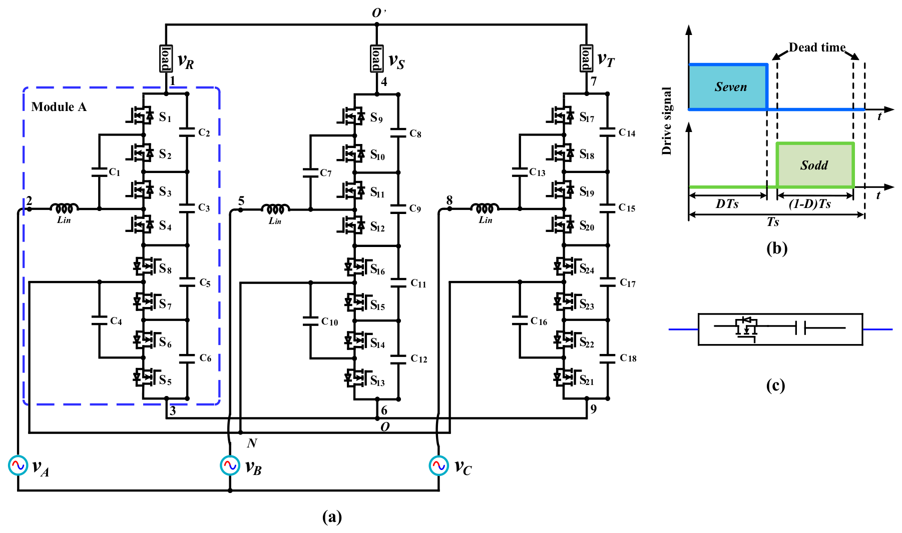
The proposed topology consists of three modules with a wye connection. The input voltages (vA, vB and vC) are connected at points 2, 5, and 8, and the load voltages (vR, vS and vT) are available at points 1, 4, and 7. Each phase is represented by one module. For instance, phase A is denoted by module A as illustrated in Figure 1a. Each module is composed of an input inductor (Lin) and two symmetrical switched capacitor cells (2 switched capacitors, 4 output capacitors and 8 switches). Therefore, the entire converter has 3 input inductors, 18 capacitors (C1~C18) and 24 switches (S1~S24). Owing to the lack of available paths for the current, direct ac/ac converters usually suffer from commutation problems, which will lead to voltage spikes across the components [41]. Hence, complex modulation strategies or snubber circuits are required to overcome this problem. Due to the absence of bidirectional switches in the proposed converter, this converter only needs a simple PWM modulation strategy to avoid the commutation problems. Consequently, the employed modulation strategy is shown in Figure 1b, in which switches Seven and Sodd are driven in a complementary manner during one switching period. Besides, a dead time is needed to prevent the shoot-through issue. Regardless of the direction of the current, there is always a current path in the converter, which can improve the reliability of this converter. Figure 1c shows the simplified symbol to denote a module.

2.2. Operation Principle

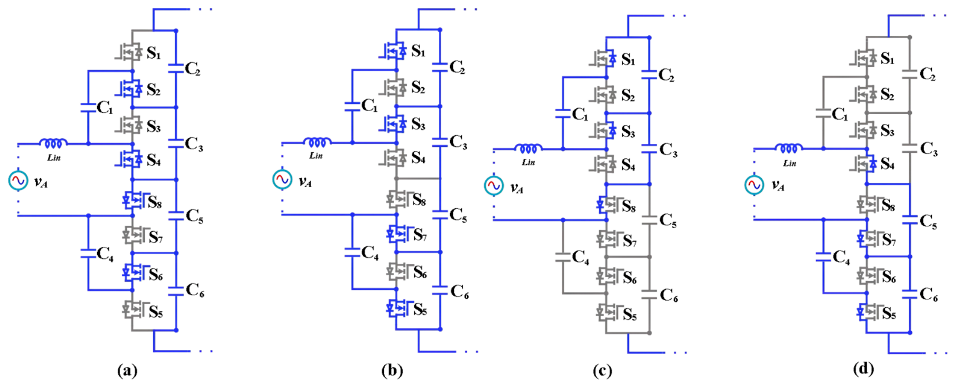
The proposed converter has the same three operational stages for each module in a switching period. Therefore, the analysis made here is only for module A during the positive half-cycle of the input voltage, which is shown in Figure 2. For thFFe negative half-cycle, module A presents the same operational stages except for the opposite current direction. The operational stages are described as follows.
Stage I (0 < t < DTs) starts when S2, S4, S6 and S8 are in the on-state while S1, S3, S5 and S7 are in off-state. The input inductor Lin is directly connected to the input voltage vA and stores the energy. The capacitor C1 is in parallel connection with C3. Similarly, the capacitor C4 is connected in parallel with C5. Capacitors C2 and C6 provide energy to the load during the whole DTs interval. Switches S2, S4, S6 and S8 are turned-off by the end of stage I.
Stage II (DTs < t < Ts) starts when S1, S3, S5 and S7 are in on-state while S2, S4, S6 and S8 are in off-state. The input inductor L releases the energy. The capacitor C1 transfers the energy to C2 and the load. The capacitor C4 is charged by C6. As capacitor C3 has been discharging the energy in stage I, it will be charged during this stage. Likewise, capacitor C5 will discharge the energy in this stage. Switches S1, S3, S5 and S7 are turned off at the end of stage II.
In order to prevent the shoot-through problem, it is crucial to add an appropriate dead time, denoted as stage III, between the above two stages. If the input inductor current is positive, the body diodes of S1, S3, and S8 can provide the circulating path for the inductor current as shown in Figure 2c. In the same way, the body diodes of S4, S5, and S7 can conduct the negative inductor current as well, which is illustrated in Figure 2d. One switching period consists of the above stages.

2.3. Operation Characteristic

By observing Figure 1a, it can be seen that the middle part of each module is a boost converter, connected with two SC cells. If parasitic parameters are ignored, the theoretical voltage gain of module A can be obtained by the combination of the voltage gains of the boost converter and two SC cells. The voltage gain of the boost converter is 1/(1 − D) and capacitors C2 and C6 are connected in series with C3 and C5 separately. Consequently, the voltage gain of module A is represented by (1). The other two modules have the same voltage gain.
G A = v 13 v A = 2 1 D
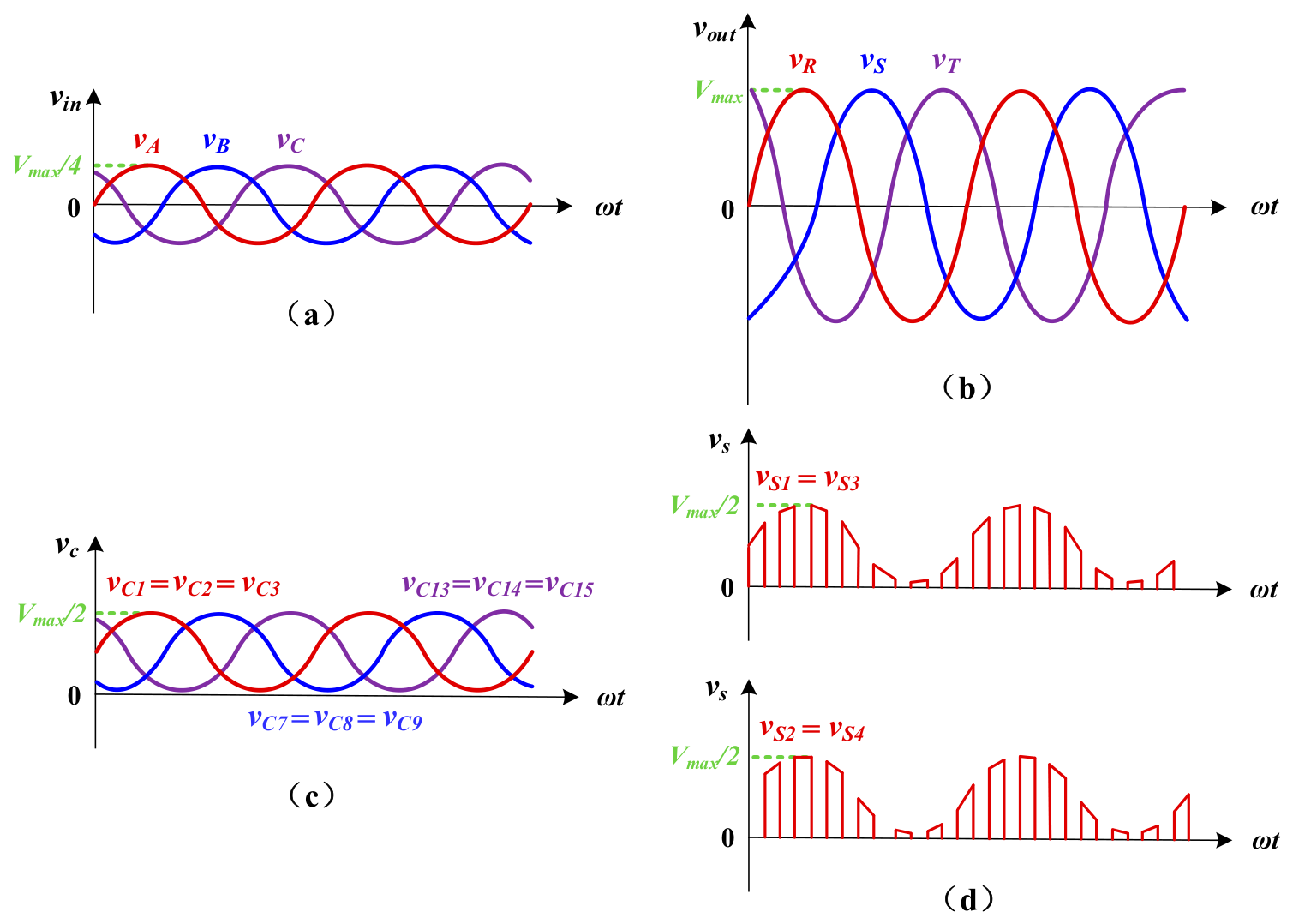
Considering the duty cycle D = 0.5, the input and output voltages of each module are shown in Figure 3, where Vmax is the maximum value of the output voltage v13. For module A, the voltage v13 is applied to capacitors C2, C3, C5 and C6. Therefore, Equations (2) and (3) can be achieved.
v c 2 + v c 3 v c 5 v c 6 = v 13
v c 2 + v c 3 + v c 5 + v c 6 = V max
As mentioned previously, the capacitor C1 will be connected to capacitors C2 and C3, respectively, within a switching period, and similarly, the capacitor C4 will be connected to capacitors C5 and C6, respectively, during the same switching period. In other words, the switched capacitor C1 can maintain the voltage balance across C2 and C3, while C4 can keep the voltage balance across C5 and C6. Therefore, the total capacitor voltages C1, C2, and C3 are equal, and the capacitor voltages C4, C5, and C6 are equal too. The operation principle of module A can also apply to modules B and C. Adding Equations (2) and (3), Equation (4) can be obtained. Subtracting Equation (2) from (3), Equation (5) can be obtained.
v c 1 = v c 2 = v c 3 = 1 4 V max + 1 4 v 13
v c 4 = v c 5 = v c 6 = 1 4 V max 1 4 v 13
As can be seen from Equation (4), each capacitor consists of an ac component v13/4 and a dc component Vmax/4. Moreover, capacitors C1, C2, and C3 are in phase with the input voltage vA. Their maximum values are equal to Vmax/2, which is another advantage of the proposed converter. In the same way, capacitor voltages C4, C5, and C6 have the same features, but they are out of phase with input voltage vA as described in Equation (5). The capacitor voltages of modules B and C are the same as those of module A, except they are phase-shifted by −120° and +120° with respect to vA, respectively, as shown in Figure 3c. All switches present the same shape as their corresponding capacitor voltages with the maximum value Vmax/2, but they are high-frequency quantities. The voltage waveforms of the switches S1, S2, S3 and S4 in module A are illustrated in Figure 3d.

2.4. Module Configuration

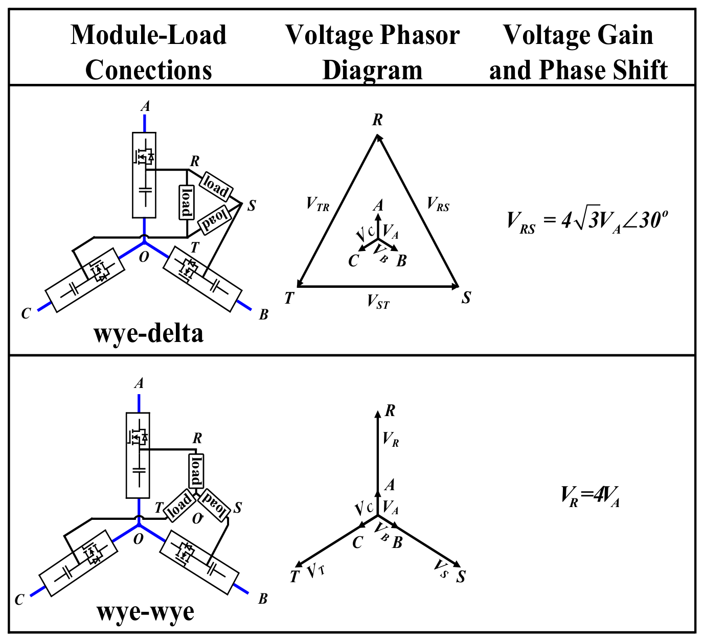
In order to maintain the differential characteristic between the input and output, the three modules can only present a wye configuration. However, the three-phase load can be connected through a delta or wye connection. Therefore, there are two possible configurations (wye-delta and wye-wye) for the proposed converter. Different module-load connections lead to different voltage phasor configurations. Considering D = 0.5, the voltage gain and phase shift between the input and output voltages are analyzed for each configuration. The detailed results are listed in Figure 4.

3. Quantitative Analysis

3.1. Operational Modes of the Proposed Three-Phase Converter

According to the charging or discharging capacitor current, the SC cell can be categorized into three operational modes: no charge (NC), partial charge (PC), and complete charge (CC) [30,31]. The CC mode indicates that the capacitor will complete the entire charging or discharging process, which leads to a high current and thereby reduces the efficiency. Hence, the CC mode is not recommended. In contrast, there is a low constant capacitor current value in NC mode, which can help improve the efficiency. Nevertheless, a large capacitor or high switching frequency is required in this mode, which will increase the costs. Capacitors are only partially charged in the PC mode. Compared to the NC mode, the PC mode demonstrates similar advantages while requiring relatively lower capacitance and switching frequency. Therefore, the PC mode is a good choice for the SC cell [36]. The charging/discharging capacitor current will approach zero within a time interval of 5τ [36,42]. τ is the time constant of the SC cell, which is represented by Equation (8). To make the proposed converter operate in PC mode, the charging or discharging time interval must be less than 5τ, yielding.
D T s 5 τ
( 1 D ) T s 5 τ
τ = ( 2 R D S ( o n ) + R E S R ) C
where RDS(on) is the conduction resistance of one MOSFET switch, RESR is the equivalent series resistance (ESR) of a capacitor, and C is the capacitance for each capacitor utilized in the converter (all equal capacitors).

3.2. Equivalent Circuit

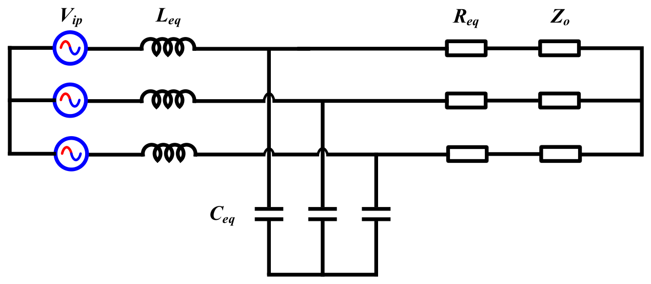
Under the condition of a balanced three-phase load, a three-phase equivalent circuit model seen by the load side with a wye-wye connection between the module and the load is established in Figure 5. This model includes the input equivalent inductors Leq, the equivalent capacitances Ceq, the equivalent resistances Req and the output loads Zo. For analytical convenience, the duty cycle D is set to 0.5. The input line-to-neutral voltage is denoted by three voltage sources vip in wye configuration, which is four times the input line-to-neutral voltage from the grid side. The resistances Req represent the conduction losses caused by SCs in each module during the charging and discharging processes [33]. Within each switching period, the voltage across the capacitor can be regarded as approximately constant.
Since the proposed converter shares the same operational process as the dc/dc SCC, its equivalent resistance Req is similar to that reported in previous studies [32,33]. As mentioned earlier, for module A, capacitor C1 is connected in parallel with C3 and C2 during DTs and (1 − D)Ts, respectively. Therefore, capacitor C1 can be equivalent to the value of DC1 and (1 − D)C1 in parallel with capacitors C3 and C2, respectively [36]. Likewise, capacitor C4 also has a value of DC4 and (1 − D)C4 to be connected to C5 and C6 separately. Considering D = 0.5 and all equal capacitors, the equivalent capacitance Ceq for each module can be obtained in this manner. The parameters of the three-phase equivalent circuit seen by the load side are listed as follows:
R e q = 1 2 f s C ( e 1 f s τ 1 ) ( 1 e D f s τ e 1 D f s τ + e 1 f s τ )
L e q = 16 L i n
C e q = 3 C 8
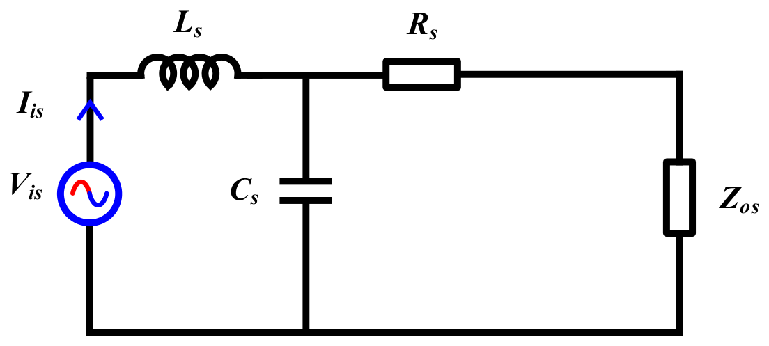
where fs is the switching frequency. To facilitate the analysis of different load connections, the proposed three-phase equivalent circuit can be simplified into a single-phase one as shown in Figure 6, where this single-phase circuit handles only one-third of the total output power. Its parameters can be calculated by using the equations mentioned above. The input voltage source is represented by vis, the conduction losses are denoted by Rs, the reactive power in the circuit is represented by Ls and Cs, and the output resistance is denoted by Zos. Their specific values are listed in Table 1.
The analysis of the equivalent circuit illustrated in Figure 6 allows the derivation of key parameters, which are crucial for designing the proposed converter and will be discussed in the next section. These parameters also provide essential insights into the performance and characteristics of the proposed converter.

3.3. Comparisons with Other SC Three-Phase AC-AC Converters

Table 2 lists some feature comparisons between the proposed converter and other converters. Due to the adoption of an additional inductor, the proposed converter can regulate the output voltage compared to other topologies. The voltage gain of each module in the proposed converter is twice that of those reported in [38,39] at the expense of more capacitors and switches (D = 0.5). The maximum voltage of the corresponding topology on the high-voltage side is represented by Vp. It can be observed from Table 2 that this paper shares the same advantage of low voltage stresses across the components with [38,39]. Moreover, another advantage of the proposed converter is the employment of unidirectional switches, which avoids the commutation problems of bidirectional switches and improves the reliability.

4. Design Considerations of the Proposed Converter

Based on the above analysis, the selection guidelines for the key parameters for the proposed converter are provided. The main specifications are as follows: output power Po = 3 kW, input line-to-neutral voltage Vin = 55 V, output line-to-neutral voltage Vout = 220 V, line frequency f = 50 Hz, input power factor PF > 0.92, and duty cycle D = 0.5.

4.1. Input Inductor Selection

The input inductor is used to reduce the ripple of the input current. In each module, the voltage across the inductor is equal to the input voltage during stage I. Therefore, the inductance Lin can be expressed as follows:
L i n = D V i n Δ i i n f s
where Δiin is the input current ripple. Considering D = 0.5, the minimum inductance can be represented by the following:
L i n 3 V i n 2 2 P o f s Δ i i n %
where Δiin% is the ratio of Δiin to the input current, which is taken the value of 0.2 in this paper.

4.2. Capacitance Calculation

Neglecting the conduction losses, the input reactive power of the proposed converter, as shown in Figure 6, can be expressed as follows:
Q i = 6 π f L s I i s 2 6 π f V o s 2 C s
Furthermore, the input power factor PF is represented by the following:
P F i = P i P i 2 + Q i 2
Based on the above equations and the requirement of the power factor, the maximum capacitance Cs can be obtained by the following:
C s = C e q 1 6 π f V o s 2 ( 6 π f L s I i s 2 + P o 1 P F i 2 P F i )
Replacing Equation (11) into (16), the maximum value for capacitors C1 to C18 can be expressed as follows:
C = 8 3 C e q 4 9 π f V o s 2 ( 6 π f L s I i s 2 + P o 1 P F i 2 P F i )
In addition, the charging or discharging time interval must be less than 5τ to ensure that the SC cells can operate in PC mode, as mentioned earlier. Considering D = 0.5 and substituting Equation (8) into (6), the minimum capacitance can be represented by the following:
C 0.1 ( 2 R D S ( o n ) + R E S R ) f s

4.3. Switches and Switching Frequency

In order to obtain a low conduction resistance, a MOSFET IPDD60R037CM8, which has an RDS(on) value of 37 mΩ, was selected to implement the unidirectional switches. By substituting the values of RDS(on), RESR and C into Equation (18), the minimum switching frequency that ensures the converter operates in PC mode can be obtained by the following:
f s min 0.1 ( 2 R D S ( o n ) + R E S R ) C
Furthermore, the feasibility of the switching frequency fs in practical implementation should also be considered. Therefore, the switching frequency fs was selected as 50 kHz.

5. Results and Discussion

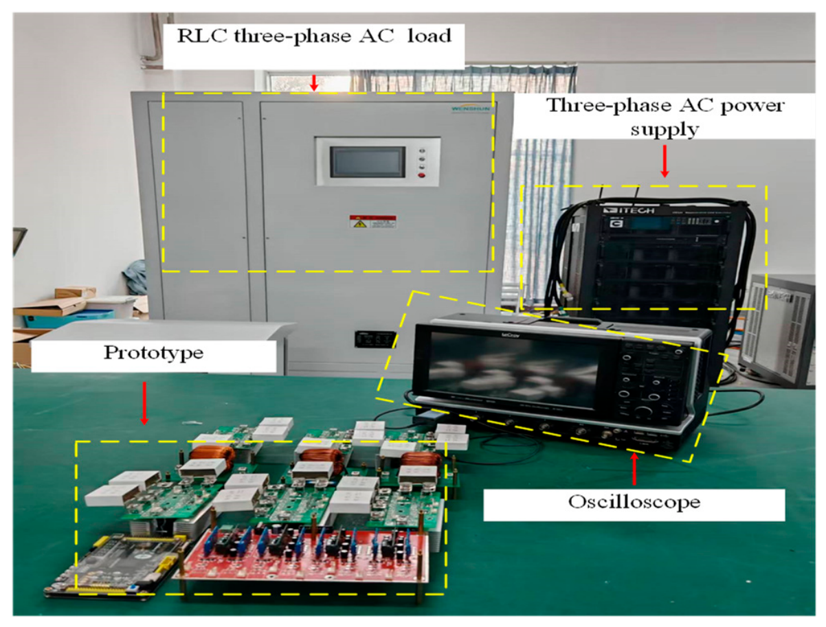
To demonstrate the previous analysis and operation of the proposed converter, a 3 kW prototype is built as shown in Figure 7. The specific experimental parameters of the prototype, which are based on the methodology in Section 3, are summarized in Table 3.
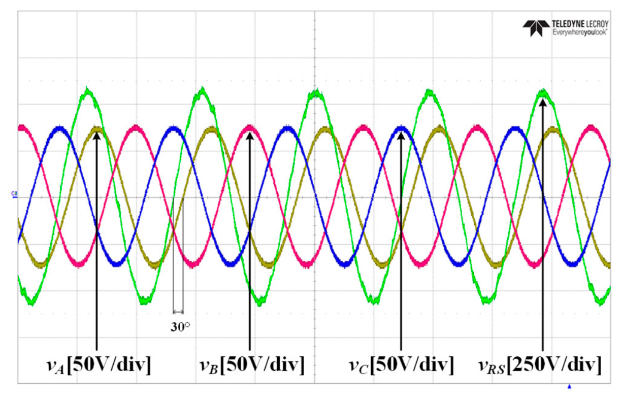
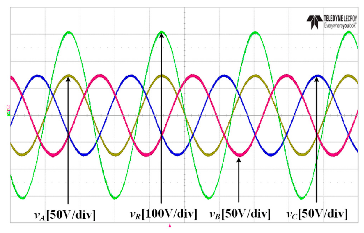
The experiments were conducted with D close to 0.5, and the input was fed by three-phase ac power. Figure 8 shows waveforms of the three line-to-neutral input voltages (vA, vB, and vC) and one output voltage (vR) for the resistive load connected in a wye configuration. The output voltage vR is in phase with the input voltage vA. Furthermore, the amplitude of vR is nearly four times that of vA at D = 0.5, which validates the voltage phase analysis in Figure 4. The line-to-neutral input voltages (vA, vB, and vC) and line-to-line output voltage (vRS) waveforms for the resistive load with delta connection are illustrated in Figure 9. As described in Figure 4, there is a 30° phase-shift between the vRS and vA, and the amplitude of vRS is 4 3 times that of vA.
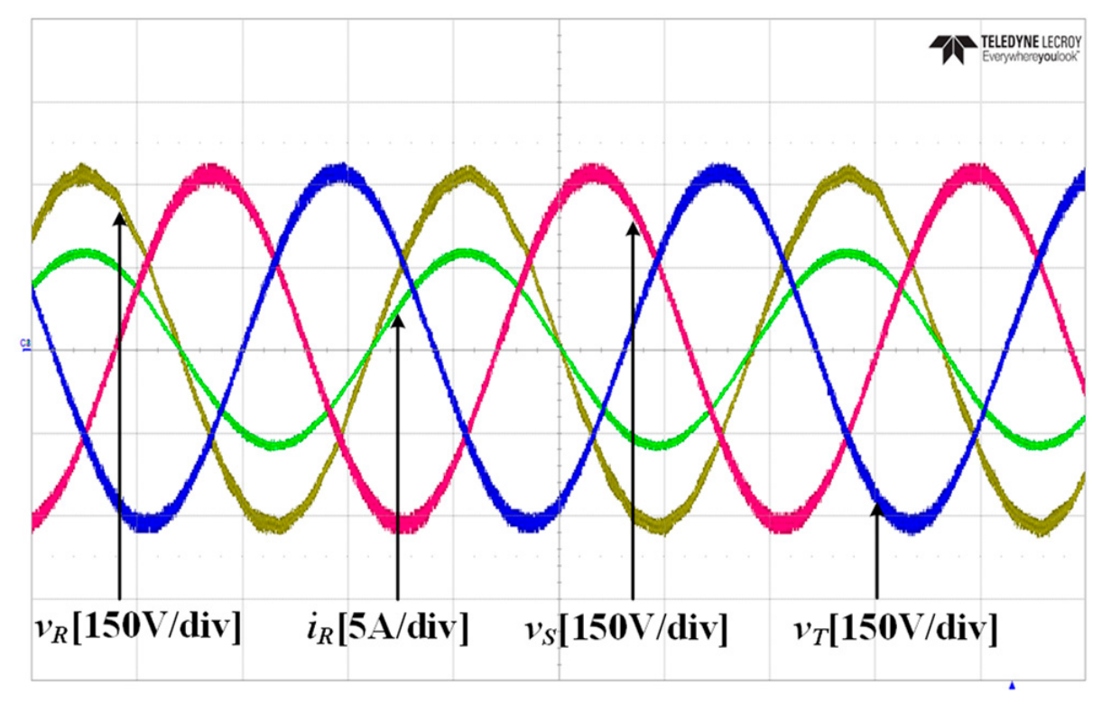
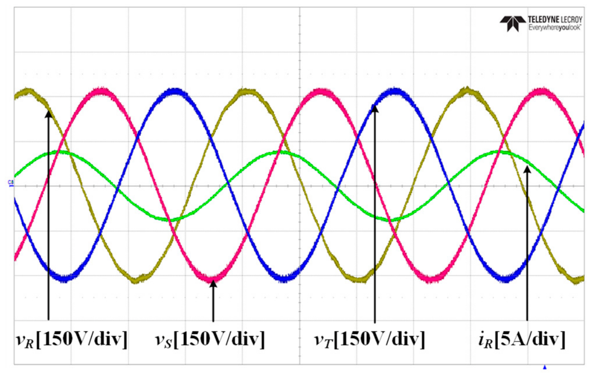
The line-to-neutral output voltages vR, vS, and vT for the resistive load with a wye connection (48 Ω per-phase) and line-to-neutral output current iR are shown in Figure 10. It can be seen that iR is in phase with vR under the resistive load. Moreover, the output voltages vR, vS, and vT are phase-shifted by 120° from each other.
Figure 11 illustrates the line-to-neutral output current iR and line-to-neutral output voltages vR, vS, and vT for the inductive load (0.61 power factor) with a wye connection. As expected, the current iR under the inductive load lags behind the output voltage vR. It has been proven that the proposed converter can also work normally under an inductive load.
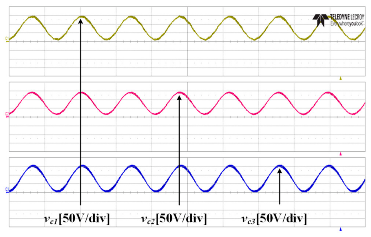
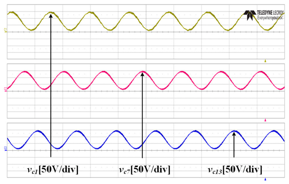
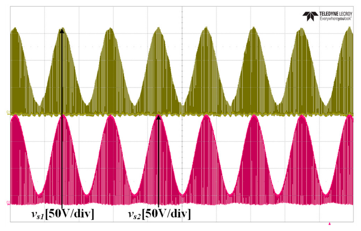
The voltage waveforms for capacitors C1, C2 and C3 in module A are shown in Figure 12. It can be observed that the capacitor voltages are approximately equal to half of the peak value of the output voltage vR, which is one of the advantages of this converter. Figure 13 shows the capacitor voltages of C1, C7, and C13. Since the capacitors are in different modules, their voltages have a phase shift of 120°. The voltages across S1 and S2 in module A are illustrated in Figure 14. Similarly, the voltage waveforms of switches exhibit the same characteristics as the corresponding capacitor voltages.
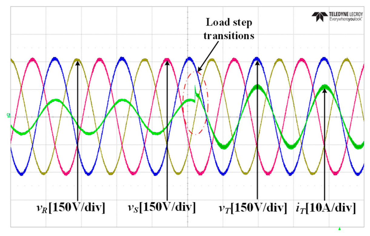
The line-to-neutral output current iT and line-to-neutral output voltages vR, vS, and vT for an unbalanced load are shown in Figure 15. Although one module handles more power than the other two (1 kW for two modules and 2 kW for one module), the line-to-neutral output voltages vR, vS, and vT can still be maintained balanced. This is due to the self-balancing capability of capacitor voltages.
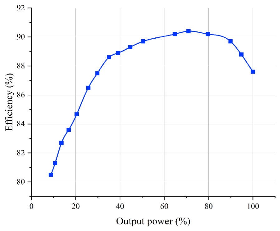
The efficiency of the proposed topology is shown in Figure 16. Figure 16 demonstrates that the peak efficiency is 90.42%. Additionally, when the converter reaches its rated power, the corresponding efficiency is 87.79%. It can be observed that the efficiency curves follow a parabolic-like trend, where the efficiency is lower at light loads, increases with the output power until it peaks, and then gradually decreases with a further increase in power.
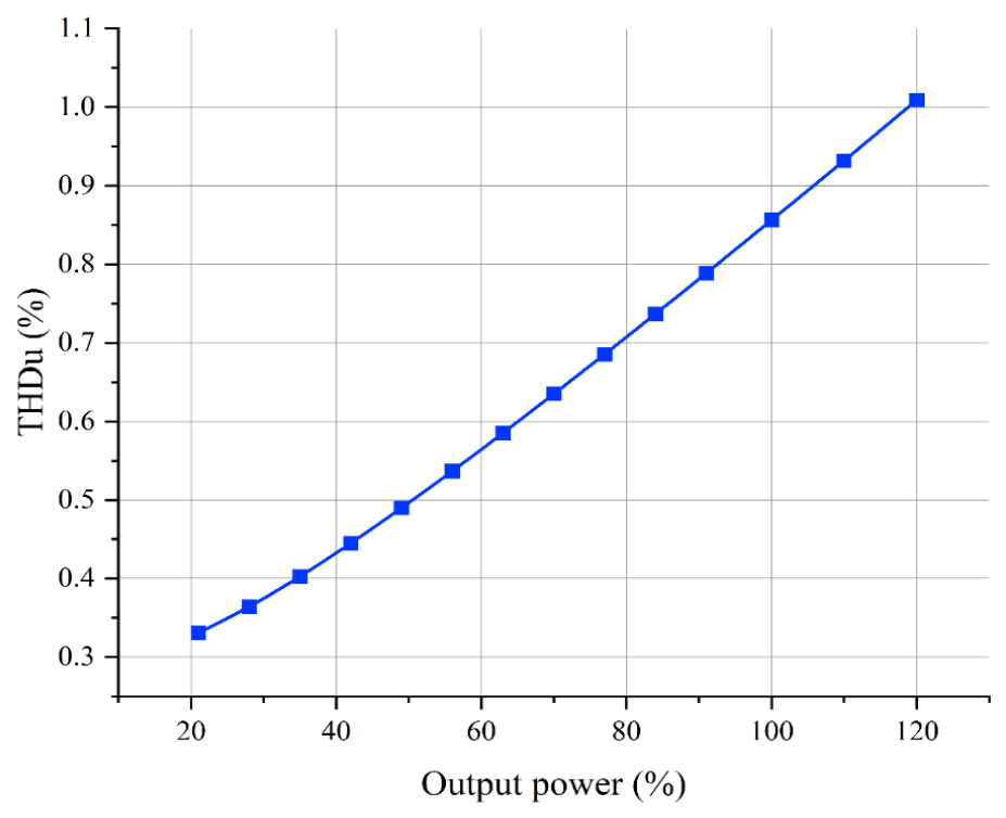
The output voltage THD of vR is measured under load variations as shown in Figure 17. As can be seen from Figure 17, the output voltage THD of vR is less than 1% over a wide range. The output voltage THD is 0.86% at rated power, demonstrating that the proposed topology has a good output voltage waveform.
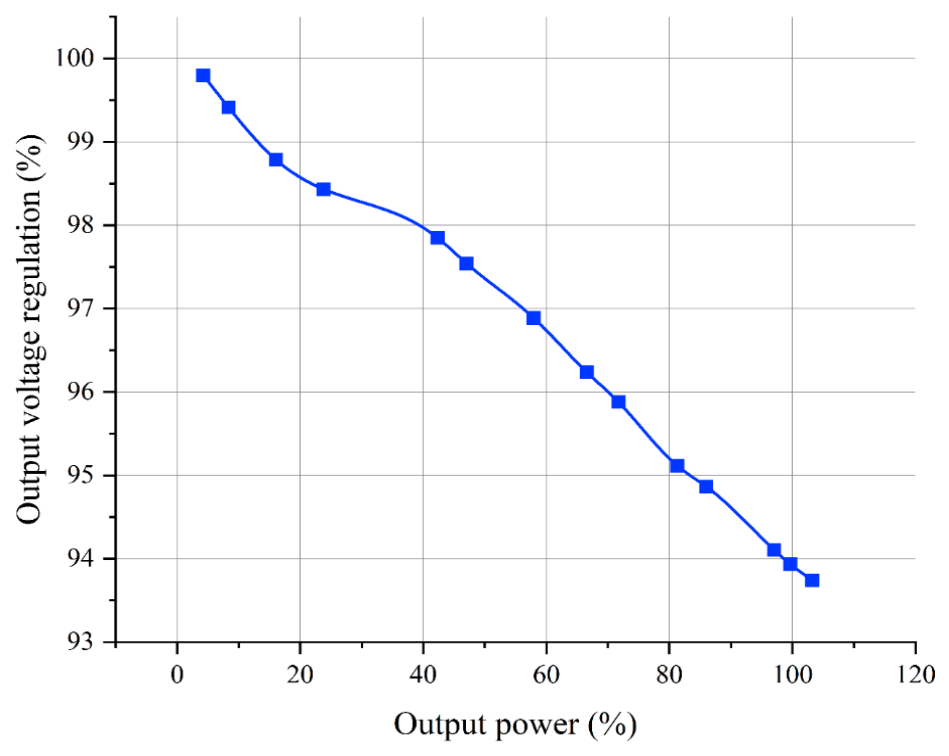
The experimental output voltage regulation curve under load variations can be seen in Figure 18. The voltage is 99.7% under no-load conditions. As the output power increases, the output voltage regulation shows a decreasing trend. The output voltage is 93.9% at rated power.
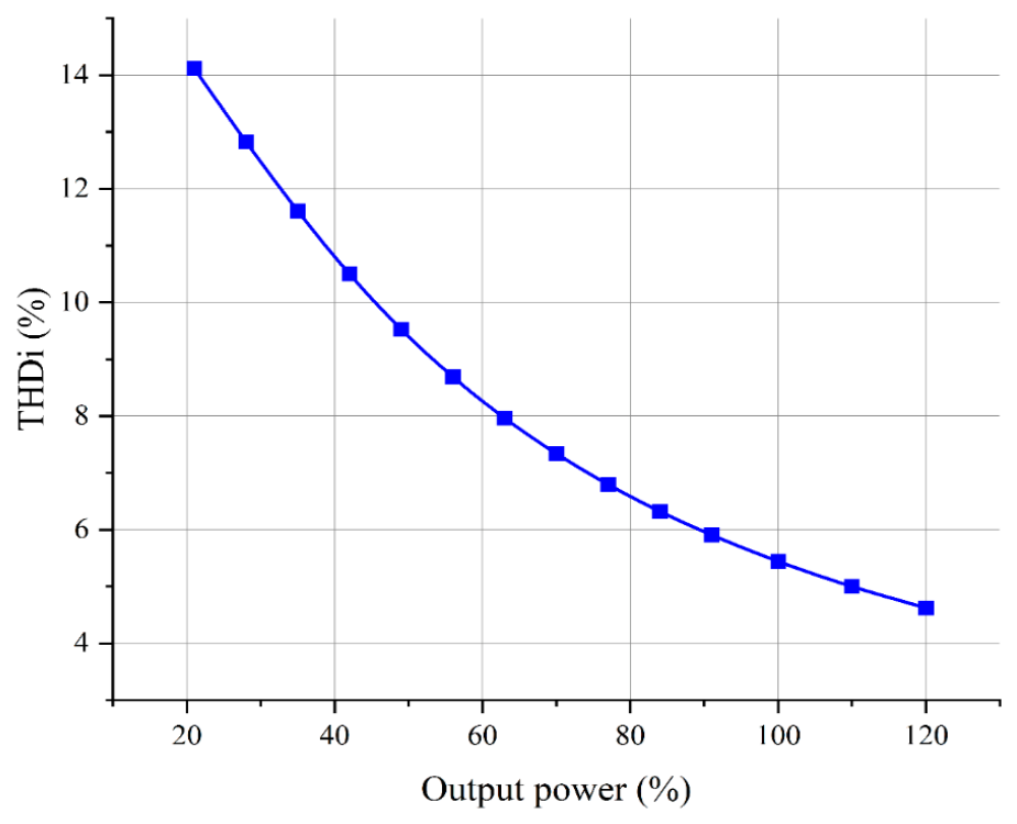
The input current THDi curve under resistive load is shown in Figure 19. As illustrated in Figure 19, at a power below 2.4 kW, the THDi is higher than 6%. At rated power, the THDi is 5.6%.
The above experimental results fully demonstrate the voltage regulation capability of this converter, and future research may explore the integration of this converter with traditional power equipment.

6. Conclusions

This paper proposes a three-phase ac/ac converter based on the SC principle. The main features of this converter are a simple modulation strategy, low voltage stresses across the components, and capacitor voltage self-balancing capability. Because of the adoption of an input inductor, this converter can adjust the output voltage. Furthermore, the employment of unidirectional switches overcomes the commutation issues of bidirectional switches. The operation principle of the converter is analyzed. Subsequently, the quantitative analysis and design considerations are conducted. At last, the experimental results verify the theoretical analysis and its advantages. The proposed converter is suitable as an alternative to the conventional three-phase autotransformer.

Author Contributions

Conceptualization, G.Y. and D.G.; methodology, G.Y.; experiment R.L.; resources, C.L.; data curation, M.H. and F.Z.; writing—original draft preparation, G.Y.; writing—review and editing, G.Y. and D.G.; funding acquisition, G.Y. and D.G.; All authors have read and agreed to the published version of the manuscript.

Funding

This research was funded by the Scientific Research Project of Jilin Province Department of Education (JJKH20261816KJ), Scientific Research Project of Jilin Province Department of Education (JJKH20250865KJ), and the National Natural Science Foundation of China (52407195).

Institutional Review Board Statement

Not applicable.

Informed Consent Statement

Not applicable.

Data Availability Statement

The data presented in this study are available on request from the corresponding author.

Acknowledgments

All authors of this paper would like to thank all the participants who have improved the quality of this work.

Conflicts of Interest

The authors declare no conflicts of interest.

References

  1. Trindade, F.C.L.; do Nascimento, K.V.; Vieira, J.C.M. Investigation on Voltage Sags Caused by DG Anti-Islanding Protection. IEEE Trans. Power Deliv. 2013, 28, 972–980. [Google Scholar] [CrossRef] [Scilit]
  2. Strasser, T.; Andrén, F.; Kathan, J.; Cecati, C.; Buccella, C.; Siano, P.; Leitão, P.; Zhabelova, G.; Vyatkin, V.; Vrba, P.; et al. A Review of Architectures and Concepts for Intelligence in Future Electric Energy Systems. IEEE Trans. Ind. Electron. 2015, 62, 2424–2438. [Google Scholar] [CrossRef] [Scilit]
  3. Newman, M.J.; Holmes, D.G.; Nielsen, J.G.; Blaabjerg, F. A dynamic voltage restorer (DVR) with selective harmonic compensation at medium voltage level. IEEE Trans. Ind. Appl. 2005, 41, 1744–1753. [Google Scholar] [CrossRef] [Scilit]
  4. Kaniewski, J.; Szczesniak, P.; Jarnut, M.; Benysek, G. Hybrid Voltage Sag\/Swell Compensators: A Review of Hybrid AC\/AC Converters. IEEE Ind. Electron. Mag. 2015, 9, 37–48. [Google Scholar] [CrossRef] [Scilit]
  5. Lo, K.Y.; Wang, W.Y. Bidirectional Isolated Single-Stage Single-Phase AC–AC Converter. IEEE J. Emerg. Sel. Top. Power Electron. 2021, 9, 6828–6836. [Google Scholar] [CrossRef] [Scilit]
  6. Nguyen, M.K.; Jung, Y.G.; Lim, Y.C. Single-Phase AC–AC Converter Based on Quasi-Z-Source Topology. IEEE Trans. Power Electron. 2010, 25, 2200–2210. [Google Scholar] [CrossRef] [Scilit]
  7. Khan, A.A.; Cha, H.; Ahmed, H.F.; Kim, H.G. Double step-down AC-AC converters with high frequency isolation. In Proceedings of the 2016 IEEE 8th International Power Electronics and Motion Control Conference (IPEMC-ECCE Asia), Hefei, China, 22–26 May 2016; IEEE: New York, NY, USA, 2016; pp. 1200–1205. [Google Scholar]
  8. da Costa, A.E.L.; Jacobina, C.B.; Rocha, N.; da Silva, E.R.C.; Lacerda Filho, A.V.d.M. A Single-Phase ac–dc–ac Unidirectional Three-Leg Converter. IEEE Trans. Ind. Electron. 2021, 68, 3876–3886. [Google Scholar] [CrossRef] [Scilit]
  9. Yang, L.; Zhao, H.; Wang, S.; Zhi, Y. Common-Mode EMI Noise Analysis and Reduction for AC–DC–AC Systems with Paralleled Power Modules. IEEE Trans. Power Electron. 2020, 35, 6989–7000. [Google Scholar] [CrossRef] [Scilit]
  10. Li, T.; Chen, J.; Cong, P.; Dai, X.; Qiu, R.; Liu, Z. Online Condition Monitoring of DC-Link Capacitor for AC/DC/AC PWM Converter. IEEE Trans. Power Electron. 2022, 37, 865–878. [Google Scholar] [CrossRef] [Scilit]
  11. Ebrahimian, A.; Vahid, S.; Weise, N.; EL-Refaie, A. Two Level AC-DC-AC Converter Design with a New Approach to Implement Finite Control Set Model Predictive Control. In Proceedings of the 2021 22nd IEEE International Conference on Industrial Technology (ICIT), Valencia, Spain, 10–12 March 2021; IEEE: New York, NY, USA, 2021; pp. 514–520. [Google Scholar]
  12. Sun, Y.; Xiong, W.; Su, M.; Li, X.; Dan, H.; Yang, J. Carrier-Based Modulation Strategies for Multimodular Matrix Converters. IEEE Trans. Ind. Electron. 2016, 63, 1350–1361. [Google Scholar] [CrossRef] [Scilit]
  13. Qiu, L.; Xu, L.; Wang, K.; Zheng, Z.; Li, Y. Research on Output Voltage Modulation of a Five-Level Matrix Converter. IEEE Trans. Power Electron. 2017, 32, 2568–2583. [Google Scholar] [CrossRef]
  14. Vijayagopal, M.; Silva, C.; Empringham, L.; de Lillo, L. Direct Predictive Current-Error Vector Control for a Direct Matrix Converter. IEEE Trans. Power Electron. 2019, 34, 1925–1935. [Google Scholar] [CrossRef] [Scilit]
  15. Jayaprakasan, S.; Ashok, S.; Ramchand, R. Analysis of Current Error Space Phasor for a Space Vector-Modulated Indirect Matrix Converter. IEEE Trans. Ind. Electron. 2022, 69, 4451–4459. [Google Scholar] [CrossRef] [Scilit]
  16. Basu, K.; Mohan, N. A Single-Stage Power Electronic Transformer for a Three-Phase PWM AC/AC Drive with Source-Based Commutation of Leakage Energy and Common-Mode Voltage Suppression. IEEE Trans. Ind. Electron. 2014, 61, 5881–5893. [Google Scholar] [CrossRef] [Scilit]
  17. Khan, A.A.; Cha, H.; Kim, H.G. Magnetic Integration of Discrete-Coupled Inductors in Single-Phase Direct PWM AC–AC Converters. IEEE Trans. Power Electron. 2016, 31, 2129–2138. [Google Scholar] [CrossRef] [Scilit]
  18. Sharifi, S.; Monfared, M.; Nikbahar, A. Highly Efficient Single-Phase Direct AC-to-AC Converter with Reduced Semiconductor Count. IEEE Trans. Ind. Electron. 2021, 68, 1130–1138. [Google Scholar] [CrossRef] [Scilit]
  19. Jong-Hyun, K.; Byung-Duk, M.; Bong-Hwan, K.; Sang-Chul, W. A PWM buck-boost AC chopper solving the commutation problem. IEEE Trans. Ind. Electron. 1998, 45, 832–835. [Google Scholar] [CrossRef] [Scilit]
  20. Kolar, J.W.; Schafmeister, F.; Round, S.D.; Ertl, H. Novel Three-Phase AC–AC Sparse Matrix Converters. IEEE Trans. Power Electron. 2007, 22, 1649–1661. [Google Scholar] [CrossRef] [Scilit]
  21. Rodriguez, J.; Rivera, M.; Kolar, J.W.; Wheeler, P.W. A Review of Control and Modulation Methods for Matrix Converters. IEEE Trans. Ind. Electron. 2012, 59, 58–70. [Google Scholar] [CrossRef] [Scilit]
  22. Empringham, L.; Kolar, J.W.; Rodriguez, J.; Wheeler, P.W.; Clare, J.C. Technological Issues and Industrial Application of Matrix Converters: A Review. IEEE Trans. Ind. Electron. 2013, 60, 4260–4271. [Google Scholar] [CrossRef] [Scilit]
  23. Hoyo, J.; Alcala, J.; Calleja, H. A high quality output AC/AC Cuk converter. In Proceedings of the 2004 IEEE 35th Annual Power Electronics Specialists Conference (IEEE Cat. No.04CH37551), Aachen, Germany, 20–25 June 2004; IEEE: New York, NY, USA, 2004; Volume 2884, pp. 2888–2893. [Google Scholar]
  24. Tang, Y.; Zhang, C.; Xie, S. Z-Source AC-AC Converters Solving Commutation Problem. In Proceedings of the 2007 IEEE Power Electronics Specialists Conference, Orlando, FL, USA, 17–21 June 2007; IEEE: New York, NY, USA, 2007; pp. 2672–2677. [Google Scholar]
  25. He, L.; Duan, S.; Peng, F. Safe-Commutation Strategy for the Novel Family of Quasi-Z-Source AC–AC Converter. IEEE Trans. Ind. Inform. 2013, 9, 1538–1547. [Google Scholar] [CrossRef] [Scilit]
  26. Ahmed, H.F.; Cha, H.; Khan, A.A.; Kim, H.G. A Family of High-Frequency Isolated Single-Phase Z-Source AC–AC Converters with Safe-Commutation Strategy. IEEE Trans. Power Electron. 2016, 31, 7522–7533. [Google Scholar] [CrossRef] [Scilit]
  27. Umeno, T.; Takahashi, K.; Oota, I.; Ueno, F.; Inoue, T. New switched-capacitor DC-DC converter with low input current ripple and its hybridization. In Proceedings of the 33rd Midwest Symposium on Circuits and Systems, Calgary, AB, Canada, 12–14 August 1990; IEEE: New York, NY, USA, 1990; Volume 1092, pp. 1091–1094. [Google Scholar]
  28. Ioinovici, A. Switched-capacitor power electronics circuits. IEEE Circuits Syst. Mag. 2001, 1, 37–42. [Google Scholar] [CrossRef] [Scilit]
  29. Ben-Yaakov, S.; Evzelman, M. Generic and unified model of Switched Capacitor Converters. In Proceedings of the 2009 IEEE Energy Conversion Congress and Exposition, San Jose, CA, USA, 20–24 September 2009; IEEE: New York, NY, USA, 2009; pp. 3501–3508. [Google Scholar]
  30. Ben-Yaakov, S. Behavioral Average Modeling and Equivalent Circuit Simulation of Switched Capacitors Converters. IEEE Trans. Power Electron. 2012, 27, 632–636. [Google Scholar] [CrossRef] [Scilit]
  31. Evzelman, M.; Ben-Yaakov, S. Average-Current-Based Conduction Losses Model of Switched Capacitor Converters. IEEE Trans. Power Electron. 2013, 28, 3341–3352. [Google Scholar] [CrossRef] [Scilit]
  32. Kimball, J.W.; Krein, P.T. Analysis and design of switched capacitor converters. In Proceedings of the Twentieth Annual IEEE Applied Power Electronics Conference and Exposition, 2005. APEC 2005, Austin, TX, USA, 6–10 March 2005; IEEE: New York, NY, USA, 2005; Volume 1473, pp. 1473–1477. [Google Scholar]
  33. Kimball, J.W.; Krein, P.T.; Cahill, K.R. Modeling of capacitor impedance in switching converters. IEEE Power Electron. Lett. 2005, 3, 136–140. [Google Scholar] [CrossRef] [Scilit]
  34. Cheung, C.K.; Tan, S.C.; Tse, C.K.; Ioinovici, A. On Energy Efficiency of Switched-Capacitor Converters. IEEE Trans. Power Electron. 2013, 28, 862–876. [Google Scholar] [CrossRef] [Scilit]
  35. Lazzarin, T.B.; Andersen, R.L.; Martins, G.B.; Barbi, I. A 600-W Switched-Capacitor AC–AC Converter for 220 V/110 V and 110 V/220 V Applications. IEEE Trans. Power Electron. 2012, 27, 4821–4826. [Google Scholar] [CrossRef] [Scilit]
  36. Andersen, R.L.; Lazzarin, T.B.; Barbi, I. A 1-kW Step-Up/Step-Down Switched-Capacitor AC–AC Converter. IEEE Trans. Power Electron. 2013, 28, 3329–3340. [Google Scholar] [CrossRef] [Scilit]
  37. Dall’Asta, M.S.; Barbi, I.; Lazzarin, T.B. AC–AC Hybrid Boost Switched-Capacitor Converter. IEEE Trans. Power Electron. 2020, 35, 13115–13125. [Google Scholar] [CrossRef] [Scilit]
  38. Lazzarin, T.B.; Andersen, R.L.; Barbi, I. A Switched-Capacitor Three-Phase AC–AC Converter. IEEE Trans. Ind. Electron. 2015, 62, 735–745. [Google Scholar] [CrossRef] [Scilit]
  39. Vecchia, M.D.; Lazzarin, T.B.; Barbi, I. A Three-Phase AC–AC Converter in Open-Delta Connection Based on Switched Capacitor Principle. IEEE Trans. Ind. Electron. 2015, 62, 6035–6041. [Google Scholar] [CrossRef] [Scilit]
  40. da Silva, R.L.; Lazzarin, T.B.; Barbi, I. Reduced Switch Count Step-Up/Step-Down Switched-Capacitor Three-Phase AC–AC Converter. IEEE Trans. Ind. Electron. 2018, 65, 8422–8432. [Google Scholar] [CrossRef] [Scilit]
  41. Shin, H.H.; Cha, H.; Kim, H.G.; Yoo, D.W. Novel Single-Phase PWM AC–AC Converters Solving Commutation Problem Using Switching Cell Structure and Coupled Inductor. IEEE Trans. Power Electron. 2015, 30, 2137–2147. [Google Scholar] [CrossRef] [Scilit]
  42. Mayo-Maldonado, J.C.; Valdez-Reséndiz, J.E.; Rosas-Caro, J.C.; Salas-Cabrera, R.; Salas-Cabrera, E.N.; Cisneros-Villegas, H. A contribution to the dynamic modeling of switched-capacitor converters. In Proceedings of the 2011 IEEE Energy Conversion Congress and Exposition, Phoenix, AZ, USA, 17–22 September 2011; IEEE: New York, NY, USA, 2011; pp. 1284–1290. [Google Scholar]
Figure 1. (a) Proposed SC three-phase ac/ac converter; (b) PWM drive signals; (c) Simplified symbol for a module.
Applsci 16 04869 g001
Figure 2. Operational stages for module A. (a) Stage I: even switches are in on-state; (b) Stage II: odd switches are in on-state. Circulating path for the inductor current iL during dead time. (c) iL > 0; (d) iL < 0.
Applsci 16 04869 g002
Figure 3. Theoretical voltage waveforms of the proposed converter. (a) Input voltages; (b) Output voltages; (c) Voltages across capacitors; (d) Voltages across switches.
Applsci 16 04869 g003
Figure 4. Analysis of voltage phasor for different module-load connections (D = 0.5).
Applsci 16 04869 g004
Figure 5. Three-phase equivalent circuit for wye-wye connection.
Applsci 16 04869 g005
Figure 6. Proposed single-phase equivalent circuit.
Applsci 16 04869 g006
Figure 7. Picture of the prototype.
Applsci 16 04869 g007
Figure 8. Experimental waveforms of output voltage vR and input voltages vA, vB and vC.
Applsci 16 04869 g008
Figure 9. Experimental waveforms of output voltage vRS and input voltages vA, vB and vC.
Applsci 16 04869 g009
Figure 10. Experimental waveforms of line-to-neutral output voltages vR, vS, and vT and line-to-neutral current iR under resistive load.
Applsci 16 04869 g010
Figure 11. Experimental waveforms of line-to-neutral output voltages vR, vS, and vT and line-to-neutral current iR under an inductive load.
Applsci 16 04869 g011
Figure 12. Experimental waveforms of voltage across capacitors C1, C2 and C3.
Applsci 16 04869 g012
Figure 13. Experimental waveforms of voltage across capacitors C1, C7 and C13.
Applsci 16 04869 g013
Figure 14. Experimental waveforms of switches S1 and S2 in module A.
Applsci 16 04869 g014
Figure 15. Experimental waveforms of line-to-neutral output voltages and line-to-neutral current for an unbalanced load.
Applsci 16 04869 g015
Figure 16. Experimental curve of efficiency.
Applsci 16 04869 g016
Figure 17. Experimental curve of output voltage THD.
Applsci 16 04869 g017
Figure 18. Experimental curve of output voltage regulation.
Applsci 16 04869 g018
Figure 19. Experimental curve of input current THD.
Applsci 16 04869 g019
Table 1. Parameters for the single-phase equivalent circuit.
Connections
(Module-Load)
visLsCsRsZos
wye-wyevipLeqCeqReqZo
wye-deltavipLeqCeqReqZo/3
Table 2. Comparisons between the proposed converter and other converters.
TopologyProposed ConverterRef.
[38]
Ref.
[39]
Ref.
[40]
Inductor count1000
Adoption of bidirectional switchesNoYesYesNo
Switch count24241612
FrequencyFixedFixedFixedFixed
Capacitor count18969
Voltage stressesVp/2Vp/2Vp/2Vp
Voltage regulationYesNoNoNo
Voltage gain2/(1 − D)2 or 0.52 or 0.52 or 0.5
Complexity of modulationLowLowLowLow
Table 3. Main specifications and components of the prototype.
ParametersQuantityValues
Input line-to-neutral voltage (vA, vB, vC)-55 Vrms
Line frequency f-50 Hz
Output power Po-3000 W
Output line-to-neutral voltage (vR, vS, vT)-220 Vrms
Switching frequency fS-50 kHz
Input inductor Lin1150 μH
Capacitors
(C1~C18)
1860 μF/4 mΩ
MOSFETs
(S1~S24)
2437 mΩ
IPDD60R037CM8
Disclaimer/Publisher’s Note: The statements, opinions and data contained in all publications are solely those of the individual author(s) and contributor(s) and not of MDPI and/or the editor(s). MDPI and/or the editor(s) disclaim responsibility for any injury to people or property resulting from any ideas, methods, instructions or products referred to in the content.