Abstract
Substrate Integrated Circuits (SICs) represent a significant advancement in microwave communication systems due to their high efficiency, performance, and integration capabilities. Empty Substrate-Integrated Waveguides (ESIWs) are a type of SIC that offers benefits such as cost-effectiveness while maintaining high performance. This paper presents the design and implementation of the first floating patch antenna integrated into an ESIW, fed by a metallic rod. The proposed antenna is designed to operate in the X-band (8–12 GHz), with a resonance peak at 10 GHz. The patch antenna is square, which provides interesting radiation characteristics. It is excited by a metallic rod that connects the patch to the ESIW line, resulting in excellent performance in terms of measured radiation efficiency (over 90%) and −10 dB impedance bandwidth (approximately 20%). The prototype demonstrates minimal differences between the simulated and manufactured versions. These results highlight the potential of ESIW-fed floating patch antennas for advanced satellite communication systems. This will enable the integration of complete communication systems within ESIWs and facilitate the straightforward development of 2D element arrays.
1. Introduction
Substrate-Integrated Circuits (SICs) are a technology designed to integrate all communication devices on a single substrate. This approach combines the advantages of both planar and non-planar circuits by embedding all communication components within one substrate, typically for use in microwave and millimetre-wave systems. Examples include Substrate-Integrated Waveguides (SIWs) [1], ESIWs [2] and Air-Filled Substrate-Integrated Waveguides (AFSIWs) [3]. ESIWs offer numerous advantages, including cost-effectiveness, light weight, simplified manufacturing, and low losses, making them ideal for various design applications [2,4]. This technology has been used to develop many passive components [5,6], but it has not been widely used for antennas.
Patch antennas are already well known, and there are numerous examples [7,8,9] with different topologies. Generally, patch antennas are implemented using dielectric substrates and fed using microstrip lines, which leads to high losses due to the dielectric material used, reduced bandwidths, and poor electrical performance. In order to avoid the aforementioned problems, the concept of a floating patch antenna fed by a metallic rod was first introduced in [10], where the patch is fed using a microstrip line (a quasi-TEM line). However, the concept of the dielectricless patch antenna was previously introduced in other works, such as [11], where a dielectric probe placed at the centre of the patch holds the floating patch, allowing the removal of almost all of the dielectric filling of the patch (the probe itself is dielectric), significantly increasing the radiation efficiency and the electrical performance. Other works [12,13] present air gaps in their patches to improve performance in terms of radiation efficiency and gain. All of them are implemented using microstrip lines, leading to an increase in losses in the feeding network.
As has been demonstrated, in order to maximise efficiency, the dielectric in the patch should be completely removed. However, to achieve even higher efficiency, it is necessary to consider the technology used to feed the patch. This feeding technology should ideally operate in an empty (air-filled) medium in order to minimise losses. Some references, such as [14,15,16,17], explore the use of empty structures for the feeding line. In [14], a configuration for feeding an ESIW dielectricless patch antenna was proposed, where a 3D-printed plastic frame supports the patch antenna, and a slot couples the electromagnetic signal to the patch. Although both the patch and feeding line are partially empty, the presence of the plastic frame affects the response, as there is a dielectric (plastic frame) between the patch and the ground plane, degrading the performance and not achieving a fully planar integration. In [15,16,17], empty structures such as ESIWs or AFSIWs are used as feeding mechanisms for patch antennas. In all of them, although the feeding structure is partially or completely empty due to the use of ESIW/AFSIW technologies, the patch itself remains filled with dielectric material, limiting their electrical response.
Thus, in this paper, we propose for the first time a completely empty floating patch antenna fed by an Empty SIW. Both structures are empty; as a result, the radiation efficiency and electrical performance are significantly improved compared to traditional antennas implemented using dielectric substrates and fed using dielectric-filled waveguides or transmission lines. In addition, the proposed antenna is implemented using standard manufacturing processes of planar technologies.
The prototype presented in this work provides a measured radiation efficiency of over 90% and a relative bandwidth of 20%. It is designed to operate in the X-band (8–12 GHz), with a resonance peak at 10 GHz. The antenna design follows the same principles as typical patch antennas [18,19], with some key differences: air replaces the dielectric, and the feeding line is a non-TEM line instead of quasi-TEM. The feeding system is quite simple and gives very good results; it also works as a holder for the patch. Other works require much more complex feeding networks with worse results in efficiency [20] or classical microstrip patch antennas [21,22] with a dielectric and its consecutive losses and reduction in bandwidth. The prototype presented shows good results in efficiency and bandwidth and has all the benefits of SIC manufacturing. This allows for the integration of full communication systems within the ESIW and the easy development of 2D element arrays.
2. Structure and Design
The prototype consists of two separate parts: the feeding line and the floating patch antenna with its rod (see Figure 1). Each part is designed, simulated, and optimised (if needed) separately, and then simulated together to validate the results (see flow chart in Figure 2). CST Studio Suite v2023 was utilised to simulate and optimise all designs.
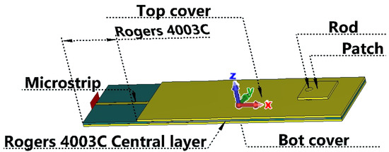
Figure 1.
Depicted ESIW prototype. Yellow represents the copper material and dark blue the dielectric substrate.
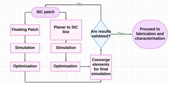
Figure 2.
Flow chart of the designing process.
2.1. ESIW
ESIW lines [2] are a modification of SIW lines [4], where the dielectric material is replaced by air, improving certain aspects of device performance, such as reducing losses while maintaining integration capabilities. A basic ESIW consists of three layers: a central layer with inner cladding where the wave travels and two covers that contain the field within the waveguide. ESIW lines operate in mono-mode status determined by the width of the waveguide a, which in this case is mm, corresponding to the WR-90 standard waveguide, covering its frequency band (8–12 GHz).
To measure the prototype, a planar-to-ESIW transition is needed. In this case, the microstrip-to-ESIW transition [23] was selected due to its high performance, making it well suited for this application. This transition affects the measurement and cannot be avoided because coaxial access is required for the Vector Network Analyser (VNA). In an integrated system within an ESIW, transitions would not be necessary, and the antenna would perform significantly better. The transition is modelled and simulated to meet the needs of the patch; since the patch does not require any special characteristics in terms of bandwidth or impedance matching, the initial simulation was sufficient, and no optimisation was needed for the transitions.
This feeding ESIW line is composed of three layers: two covers (top and bottom) made of FR-4 substrate and a central layer made of Rogers 4003C substrate, with respective heights of 0.8 mm (hcover) and 0.813 mm (hro).
2.2. Patch
Standard patch antenna design principles [18,19] are useful as an initial design point; however, the patch must be adapted to a non-TEM line. This is carried out by adding some distance from the rod to the end of the waveguide, denoted as lshort, and displacing the feeding point of the rod with respect to the edge of the patch, denoted as Apatch (see Figure 3), which will be explained in the next subsection. The patch is a square patch ( = ), implemented using FR-4 substrate (0.8 mm height) with metallised walls (see Equation (1) from [18], which proposes equations to calculate the length () and width () of a square microstrip patch particularised to an air substrate ( = 1)). is the displacement of the centre of the rod with respect to the patch edge (see Figure 4).
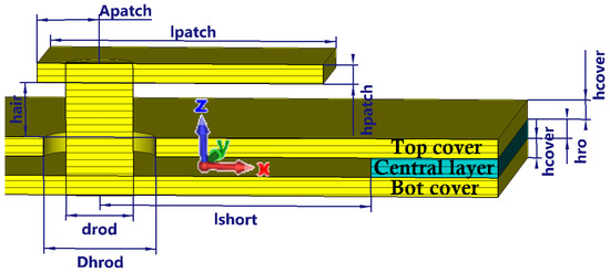
Figure 3.
Inner cut of ESIW patch with parameters.
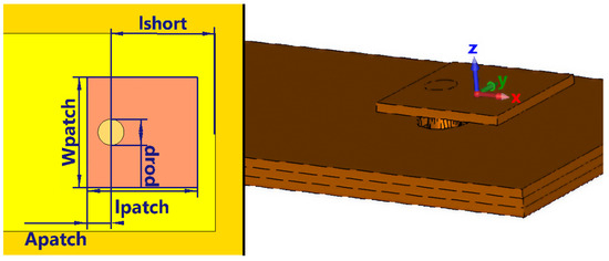
Figure 4.
Frontal view without the top cover. In orange is the patch (copper), in light orange the rod (copper), in yellow (copper) the bot cover, and in dark yellow the central layer (copper) [left] and patch positioning [right].
Here, is the the speed of light (299,792,458 m/s), f the resonance frequency of the antenna (10 GHz), the relative permittivity (1 for air), the effective permittivity (see Equation (2)), the permittivity of free space, the magnetic permeability of a vacuum, and h the height of the substrate (0.818).
Once and are calculated, the integration can be accomplished.
2.3. ESIW Integration
The rod is placed in the middle width of the ESIW line () because this is where the electric field is maximum and allows for the symmetrisation of the radiation pattern. The ESIW ends in a short circuit, generating a standing wave. To achieve the maximum electric field, the rod must be placed at a distance of /4 from the short circuit, converting it into a virtual open circuit, and thus obtaining the maximum electric field. Initially, lshort equals , proving to be a good starting point for optimisation for the patch (see Figure 4).
The rod must go through the patch and the ESIW line, as shown in Figure 3. To achieve this, a hole slightly wider than drod has to be made in the patch, allowing the rod to pass through without removing the metallisation of the hole (see Figure 3). Then, another hole in the top cover with a diameter Dhrod is needed. This hole must be large enough to prevent shortcuts between the rod and the cover, but not so large as to allow the field to escape. In the bottom cover, another hole similar to the one used in the patch has been included; it must be slightly wider than drod. To achieve electrical continuity, the post is welded at the junction with the bottom cover.
Simulations have shown that the diameters of the rod (drod) and hole (Dhrod) have minimal impact as long as they remain small compared to the length of the patch. Therefore, both parameters are arbitrary and have been set to a diameter available in the laboratory for the rod and an easy-to-manufacture value for the hole diameter.
2.4. Optimisation
For optimisation, the following parameters were chosen: Lpatch = Wpatch, lshort, and Apatch. Initially, Lpatch equalled /2 and lshort equalled /4, as explained before. Apatch initially equalled (to keep the rod inside the patch) plus a small displacement; in this case, a displacement of 1 mm was chosen ( mm). In [24], the initial position with respect to the edge for feeding the patch antenna is explained. The impedance () and bandwidth depend on the shape factor (which is 1 in this case, as ) and the feeding point, denoted as . Variations in the cavity volume alter the total amount of energy that can be stored between the patch and the ground plane.
The chosen algorithm was the Trust Region Algorithm, with the goals of maximising the resonance peak at the operating frequency (10 GHz) and achieving a 20% bandwidth. In order to manufacture the prototype, the value of was discretised using substrate heights available in the laboratory. Therefore, , where is the number of stacked substrates and the heights of them. Initially, an arbitrary value of N was selected in order to compute (see Figure 3). Then, the design parameters (, , and ) were optimised to minimise the reflection coefficient at the operating frequency while covering the required bandwidth. If the resulting bandwidth was insufficient, the value of N was increased (by adding a layer), and the design procedure was repeated—applying the same optimisation goal—until was sufficient to cover the required bandwidth (variations in efficiency are negligible with different values of hair). Finally, the value hair = 2.439 mm was chosen because it is an integer multiple of 0.813 mm (the height of the Rogers 4003C substrate), which facilitates the subsequent assembly of the patch, provides the required bandwidth, and acceptable values of bandwidth and gain. All the final parameters after the different optimisations mentioned above are summarised in Table 1. CST Studio Suite 2023 was the software used to optimise them. This device provides a 20% bandwidth, 8.2 dBi gain, and radiation efficiency over 90% in simulation.

Table 1.
Summarised parameters after optimisation, with , , , and being the design parameters.
3. Manufacturing Procedure
In order to validate the proposed patch, a prototype utilising the aforementioned dimensions has been manufactured. The manufacturing procedure follows the guidelines for SIC circuits, with a few specific characteristics.
The welding procedure, while relatively straightforward, must be executed with care by following the following steps:
- (1)
- Weld the ESIW circuit using standard methodologies for SICs.
- (2)
- Weld the rod to the bottom cover using a welder and a small amount of tin paste along the joint. Flux can help the tin paste to spread while welding.
- (3)
- Weld the patch to the rod using a welder and a small amount of tin paste along the joint.
These prototypes are highly sensitive to height variations and tilting, making it crucial to ensure the correct height for the patch. In Figure 5, the patch welded to the rod can be seen once the prototype is assembled. Several parametric simulations have been conducted to analyse manufacturing tolerances. A variation of 16.67% in the distance between the patch and the ground results in approximately a 5% change in BW−10dB and a 6% change in gain. Variations in the tilting angle can reduce bandwidth by up to 4.7%, with a rotation angle of degrees. Note that tilting will also produce non-symmetric radiating patterns; this tilting affects two axes, the XZ plane and the YZ plane (see Figure 4), because they break the parallelism between the patch and the top cover.
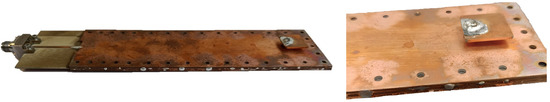
Figure 5.
Manufactured prototype (left) and welded patch detail (right).
To avoid the aforementioned effects, the following process between the feed post and the patch should be considered: The patch was placed on a stack of substrates that matched the simulated height. Pressure was applied during soldering to ensure the patch remained parallel to the ground plane, preventing tilting. After soldering, the stack of substrates was removed.
Given the wide range of substrate height options available on the market, the height can be adjusted to meet specific antenna requirements. Based on various simulations, it is important to note that increasing the distance between the patch and the ground plane increases bandwidth but decreases directivity, and vice versa. This height was constrained to a discrete value determined by combinations of available substrates in the laboratory: the selected height was 2.439 mm, achieved using three layers of Rogers 4003C substrate, each with a thickness of 0.813 mm.
Another possible source of error is the rotation in the XY plane (see Figure 4) of the patch (negligible according to simulation) or soldering faults (easily avoidable with careful soldering). The patches are slightly bevelled at their corners because, in order to be metallised, patches must have some kind of support. In these structures, die cuts are used to achieve this. The effect on the antenna performance is negligible.
Yield analysis with typical manufacturing errors ( µm) for the potential error parameters (hair, lshort, Wpatch, Apatch, and Lpatch) proves that 97.6352% of the devices maintain over 18% bandwidth for the ESIW patch, demonstrating manufacturing robustness.
4. Results
The manufactured prototype is shown in Figure 5, while the comparison of the measured and simulated reflection coefficients is presented in Figure 6. The initial results without the microstrip–ESIW transition have been included (denoted as simulated no transition). It can be observed that the measured −10 dB impedance bandwidth achieves a value of 19%, which is very close to the simulated value of 20%, probably due to a small deviation in hair during welding, as explained before.
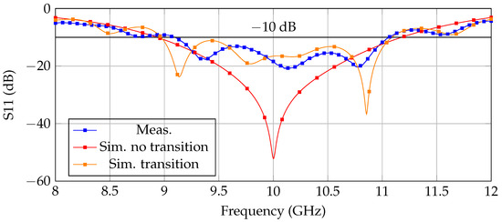
Figure 6.
Measured and simulated of the proposed antenna. The reflection coefficient of the patch without the transition has been included.
The difference in the parameter between the simulated and prototype (Figure 6) is due to the presence of the previously mentioned transition from planar to SIC, which produces resonances along the working band due to small impedance mismatches. If we compare the measured results with a simulation of the patch with the microstrip-to-ESIW transition, it can be seen that they are very similar. This confirms that the transition degrades the original response of the patch shown in Figure 6. In an integrated ESIW system, the transition would not be necessary, and the performance with a pure ESIW feed would be recovered.
The measured radiation efficiency reaches 90.48% at the central frequency (10 GHz) once the microstrip and connector losses have been removed, closely matching the simulation results. At 9 GHz, this efficiency is 80.77%, and 80.11% at 11 GHz, exceeding 80% efficiency along the bandwidth, again, once the microstrip and connector losses have been removed. To remove these losses, a stand-alone microstrip was manufactured and measured with the same length as that of the feeding line, so that the losses of the feeding can be deduced from the measured S21 parameter of the line.
The radiation characteristics are shown in Figure 7 and Figure 8, showing minimal differences between the simulated and measured results, proving the robustness of the manufacturing method. The beam width at −3 dB is around 40° for both the XZ and XY cuts. The copolar-to-crosspolar ratio is quite low within the −3 dB beam width, exceeding 20 dB. In Figure 9, the antenna and anechoic chamber can be seen. To compute the gain and measured efficiency, the comparison method was used [25], with the horn antenna DRH40 as the reference. In Table 2, a comparison with other similar devices is presented. The proposed ESIW device demonstrates a bandwidth of 19% at a centre frequency of 10 GHz, with a measured radiation efficiency of 90.48% and a directivity of 8.11 dBi. Comparing these results with other devices, the [10] device has less bandwidth and similar radiation efficiency (96%) but higher directivity (9.63 dBi). This antenna uses floating microstrip technology (not a complete integration), so it is not integrated with an ESIW line. This is not significant for a single antenna and a short microstrip feed. However, if this patch is used to develop an array, the microstrip feeding network will introduce more loss than ESIW feeding, and the efficiency of the ESIW integrated array will be notably higher than that of the equivalent array fed with a microstrip.
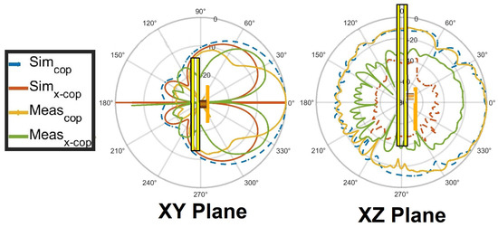
Figure 7.
Normalised radiation farfield cuts at 10 GHz (simulated and measured).
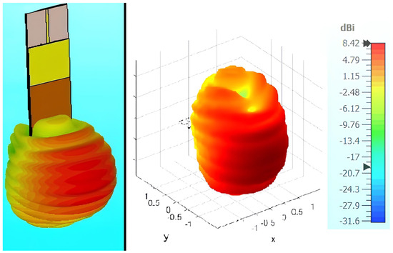
Figure 8.
Three−dimensioanl E−field radiation pattern simulated (left) vs measured (right).
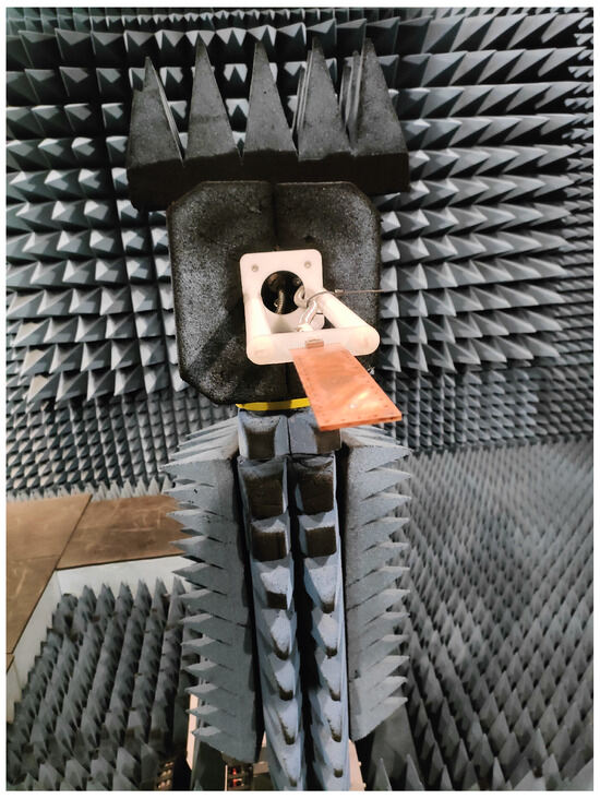
Figure 9.
Measurement of the patch in anechoic chamber.
Table 2.
Comparative table.
The structure reported in [26] presents a lower bandwidth, efficiency, and directivity, with this antenna being integrated in the microstrip. A single-layer, dual-polarised, high-gain cross-patch microstrip antenna is presented in [27]; it has a lower bandwidth, similar efficiency, and higher directivity. The [14] device shows a lower bandwidth, similar efficiency, and lower directivity, using slot integration technology; also, the main difference is that the proposed work has been fully integrated in an ESIW and is fed by a rod, not by a coupled slot. Finally, the device presented in [28] has a lower bandwidth and similar radiating efficiency and directivity using AFSIW technology. As previously explained, it is important to consider that a greater height between the ground plane and the patch results in lower directivity. This explains why the directivity of the proposed antenna is lower compared to the works presented in [10,27]. However, despite this difference in directivity, the presented antenna demonstrates an outstanding compromise among the key figures of merit, bandwidth, efficiency, and directivity, showcasing excellent bandwidth.
5. Conclusions
A high-efficiency, wide-bandwidth empty patch antenna integrated into an ESIW has been proposed for space applications. It utilises an empty patch with a rod and is fed using an ESIW line to achieve a radiation efficiency of at least 90% at the operating frequency and a -10 dB impedance bandwidth of 19%. The proposed patch is the first floating patch held by a metallic rod and fed by an ESIW without supports or external elements that degrade the response. There is very little difference between the manufactured and simulated prototypes, showcasing the good and easy manufacturing method. In addition, yield and parametric analysis prove that the device is quite robust to manufacturing errors, while the most likely error sources have been traced and mitigated. Compared to other similar patches, it offers a superior compromise between bandwidth, directivity, and efficiency, with remarkable values in both bandwidth and efficiency. Additionally, it is easy to manufacture, small, and provides a robust patch placement, making it particularly suitable for applications requiring high efficiency and performance across a broad frequency range. This opens the possibility to develop high-performance array antennas fully integrated in ESIWs and with exceptional efficiency.
All of these factors prove that floating patches fully integrated into SICs are very convenient for microwave satellite communications. This will allow the development of high-performance array antennas with low-loss ESIW feeding, enabling full communication systems integrated into SIC circuits, making them exceptional for the next satellite generation.
Author Contributions
Conceptualization, A.B., M.D.F. and A.A.; methodology, A.B., M.D.F. and A.A.; software, M.D.F. and D.H.T.; validation, A.B., M.D.F., D.H.T., I.G.C., D.H.-Z. and A.A.; formal analysis, A.B.; investigation, D.H.T. and A.A.; resources, A.B.; data curation, D.H.T. and D.H.-Z.; writing—original draft preparation, D.H.T.; writing—review and editing, A.B., M.D.F., D.H.T., I.G.C. and D.H.-Z.; visualization, D.H.T. and D.H.-Z.; supervision, A.B., M.D.F. and A.A.; project administration, A.B.; funding acquisition, A.B. All authors have read and agreed to the published version of the manuscript.
Funding
This work was partially supported by the coordinated Research Project PID2022-136590OB, Subproject C44, funded by MICIU/AEI/10.13039/501100011033, Spanish Government, and by ERDF A way of making Europe, EU, and partially supported by the coordinated Research Project TED2021-129196B, Subproject C44, funded by MICIU/AEI/10.13039/501100011033, Spanish Government, and by the European Union NextGenerationEU/PRTR. This work was developed thanks to the European social fund ESF+.
Institutional Review Board Statement
Not applicable.
Informed Consent Statement
Not applicable.
Data Availability Statement
The original contributions presented in the study are included in the article, further inquiries can be directed to the corresponding author.
Acknowledgments
Gamma research group.
Conflicts of Interest
The authors declare no conflicts of interest.
Abbreviations
The following abbreviations are used in this manuscript:
| SIC | Substrate Integrated Circuit |
| ESIW | Empty Substrate Integrated Waveguide |
| BW−10dB | Bandwidth at −10 dB |
References
- Deslandes, D.; Wu, K. Integrated microstrip and rectangular waveguide in planar form. IEEE Microw. Wirel. Components Lett. 2001, 11, 68–70. [Google Scholar] [CrossRef]
- Belenguer, A.; Esteban, H.; Boria, V.E. Novel empty substrate integrated waveguide for high-performance microwave integrated circuits. IEEE Trans. Microw. Theory Tech. 2014, 62, 832–839. [Google Scholar] [CrossRef]
- Parment, F.; Ghiotto, A.; Vuong, T.-P.; Duchamp, J.-M.; Wu, K. Air-filled substrate integrated waveguide for low-loss and high power-handling millimeter-wave substrate integrated circuits. IEEE Trans. Microw. Theory Tech. 2015, 63, 1228–1238. [Google Scholar] [CrossRef]
- Wu, K.; Deslandes, D.; Cassivi, Y. The substrate integrated circuits—A new concept for high-frequency electronics and optoelectronics. In Proceedings of the 6th International Conference on Telecommunications in Modern Satellite, Cable and Broadcasting Service, 2003, TELSIKS 2003, Nis, Yugoslavia, 1–3 October 2003; p. P-III. [Google Scholar] [CrossRef]
- Haghirosadat, S.H.; Neshati, M.H. Development a wideband ESIW H- plane horn antenna with improved radiation performance. In Proceedings of the 2020 28th Iranian Conference on Electrical Engineering (ICEE), Tabriz, Iran, 4–6 August 2020; pp. 1–5. [Google Scholar]
- Qi, Z.; Li, X.; Xiao, J.; Zhu, H. Low-cost empty substrate integrated waveguide slot arrays for millimeter-wave applications. IEEE Antennas Wirelesfs Propag. Lett. 2019, 18, 1021–1025. [Google Scholar] [CrossRef]
- Sharma, S.; Kumar, M.; Nigam, H.; Mathur, M. Dual band circular patch coplaner microstrip patch antenna for x band and ku band applications. In Proceedings of the 2021 IEEE Indian Conference on Antennas and Propagation (InCAP), Rajasthan, India, 13–16 December 2021; pp. 344–346. [Google Scholar]
- Yang, F.; Zhang, X.-X.; Ye, X.; Rahmat-Samii, Y. Wide-band e-shaped patch antennas for wireless communications. IEEE Trans. Antennas Propag. 2001, 49, 1094–1100. [Google Scholar] [CrossRef]
- Mathew, S.; Anitha, R.; Deepak, U.; Aanandan, C.K.; Mohanan, P.; Vasudevan, K. A compact tri-band dual-polarized corner-truncated sectoral patch antenna. IEEE Trans. Antennas Propag. 2015, 63, 5842–5845. [Google Scholar] [CrossRef]
- Fernandez, M.D.; Herraiz, D.; Herraiz, D.; Alomainy, A.; Belenguer, A. Design of a wide-bandwidth, high-gain and easy-to-manufacture 2.4 GHz floating patch antenna fed with the through-wire technique. Appl. Sci. 2022, 12, 12925. [Google Scholar] [CrossRef]
- Belamgi, S.B.; Ray, S.; Das, P. Suspended planar patch antenna for wireless energy transfer at 2.45 GHz. In Proceedings of the International Conference on Electronics, Communication and Instrumentation (ICECI), Kolkata, India, 16–17 January 2014; pp. 1–4. [Google Scholar]
- Kharusi, K.; Ramli, N.; Noor, S.; Ali, M.T.; Hazwan, M. Gain enhancement of rectangular microstrip patch antenna using air gap at 2.4 GHz. Int. J. Nano Biomater. 2020, 13, 211–224. [Google Scholar]
- Verma, R.; Saxena, N.; Pourush, P. Effect of air-gap technique in bandwidth of microstrip patch array antenna. JournalNX 2021, 3, 165–168. [Google Scholar]
- Fernandez, M.D.; Herraiz, D.; Herraiz, D.; Alomainy, A.; Belenguer, A. Dielectricless floating-patch antenna at 28 GHz fed with an empty substrate integrated waveguide. IEEE Access 2023, 11, 6559965607. [Google Scholar] [CrossRef]
- Ding, T.; Wang, M.; Kou, A.; Han, C.-Z.; Xiao, J. High-gain circularly polarized array antenna based on high-order mode ESIC for 5G millimeter-wave application. IEEE Antennas Wirel. Propag. Lett. 2024, 23, 3063–3067. [Google Scholar] [CrossRef]
- Qi, Z.; Shi, M.; Li, K.; Wang, D.; Jiang, X.; Li, X. Hybrid modes based wideband dual-polarized empty substrate integrated waveguide antenna for 5G applications. IEEE Antennas Wirel. Propag. Lett. 2024, 24, 103–107. [Google Scholar] [CrossRef]
- Nguyen, N.-H.; Ghiotto, A.; Le, M.T.; Vuong, T.-P. High gain microstrip patch antenna array using air-filled substrate integrated waveguide (AFSIW) feeding structure. In Proceedings of the 2022 International Conference on Advanced Technologies for Communications (ATC), Ha Noi, Vietnam, 20–22 October 2022; pp. 54–57. [Google Scholar]
- Balanis, C.A. Antenna Theory: Analysis and Design; Wiley Interscience: Hoboken, NJ, USA, 2005. [Google Scholar]
- Carver, K.; Mink, J. Microstrip antenna technology. IEEE Trans. Antennas Propag. 1981, 29, 2–24. [Google Scholar] [CrossRef]
- Wang, S.; Zhang, K.; Li, L.; Tian, B. A probe-fed stacked U-slot patch antenna for satellite applications. In Proceedings of the 2017 International Applied Computational Electromagnetics Society Symposium (ACES), Suzhou, China, 1–4 August 2017; pp. 1–2. [Google Scholar]
- Sulistyaningsih; Putranto, P.; Wahab, M.; Estu, T.T. Microstrip patch array antenna with inset fed and perturbation for a 3 GHz S-band coastal radar. In Proceedings of the 2017 International Conference on Radar, Antenna, Microwave, Electronics, and Telecommunications (ICRAMET), Jakarta, Indonesia, 23–24 October 2017; pp. 174–179. [Google Scholar]
- Darsono, M.; Wijaya, A.R. Design and simulation of a rectangular patch microstrip antenna for the frequency of 28 GHz in 5G technology. J. Phys. Conf. Ser. 2020, 1469, 012107. [Google Scholar] [CrossRef]
- Esteban, H.; Belenguer, A.; Sánchez, J.R.; Bachiller, C.; Boria, V.E. Improved low reflection transition from microstrip line to empty substrate-integrated waveguide. IEEE Microw. Wirel. Components Lett. 2017, 27, 685–687. [Google Scholar] [CrossRef]
- Lee, T.H. Planar Microwave Engineering: A Practical Guide to Theory, Measurement, and Circuits; Cambridge University Press: Cambridge, UK, 2004. [Google Scholar]
- Laport, E.A. Radio Antenna Engineering; McGraw-Hill: Singapore, 1952. [Google Scholar]
- Muntoni, G.; Montisci, G.; Casula, G.A.; Chietera, F.P.; Michel, A.; Colella, R.; Catarinucci, L.; Mazzarella, G. A curved 3-D printed microstrip patch antenna layout for bandwidth enhancement and size reduction. IEEE Antennas Wirel. Propag. Lett. 2020, 19, 1118–1122. [Google Scholar] [CrossRef]
- Chen, C. A single-layer single-patch dual-polarized high-gain cross-shaped microstrip patch antenna. IEEE Antennas Wirel. Propag. Lett. 2023, 22, 2417–2421. [Google Scholar] [CrossRef]
- Messem, L.V.; Moerman, A.; Caytan, O.; Rogier, H.; Lemey, S. Substrate-integrated coaxial line fed air-filled SIW antenna for the 28 GHz 5G bands. In Proceedings of the 2024 54th European Microwave Conference (EuMC), Paris, France, 24–26 September 2024; pp. 453–456. [Google Scholar]
Disclaimer/Publisher’s Note: The statements, opinions and data contained in all publications are solely those of the individual author(s) and contributor(s) and not of MDPI and/or the editor(s). MDPI and/or the editor(s) disclaim responsibility for any injury to people or property resulting from any ideas, methods, instructions or products referred to in the content. |
© 2025 by the authors. Licensee MDPI, Basel, Switzerland. This article is an open access article distributed under the terms and conditions of the Creative Commons Attribution (CC BY) license (https://creativecommons.org/licenses/by/4.0/).