Abstract
Wireless sensor networks (WSNs) for self-driving vehicles are growing rapidly, requiring high-performance radar systems with strong communication abilities. The key component of these systems is the voltage-controlled oscillator (VCO), which performs at 24 GHz with low phase noise, low power consumption, and a wide range of tuning. In this paper, the adaptive particle swarm optimization (PSO) algorithm incorporates adaptive scaling to speed up the optimization process. The new adaptive PSO minimizes the number of calculations required for complex engineering problems where rapid optimization is crucial and finding the best solution quickly is important. In order to test the adaptive PSO, benchmark functions are used. When applied to the proposed VCO circuit design, it facilitates more efficient adjustment of component values and improved performance, resulting in faster optimization. This optimized VCO achieves low phase noise of −120 dBc/Hz with a 1 MHz offset and a tuning range of 21.2%, operates at just 0.9 V, and consumes just 1.35 mW of power. A comparison of adaptive PSOs with traditional PSO methods shows that they improve the performance of the VCO, making them a promising choice for future automotive radar systems.
1. Introduction
Wireless sensor networks (WSNs) are increasingly being used to solve challenges related to the scalability, range, and speed of data transfer by integrating 5G technology. The fifth generation of wireless communication, 5G, provides a number of major benefits, including ultra-low latency (as low as 1 millisecond), extremely high data rates (up to 10 Gbps), and the ability to support many devices at the same time [1].
Traditional WSNs often rely on short-range communication technologies to relay data across a large area, which requires a number of gateway nodes placed closely together to relay the information, as shown in Figure 1 [2,3]. To support the high data rates required by 5G wireless transmitters and receivers, the most suitable choice is made by millimeter-wave frequency bands (ranging from 24 GHz to 86 GHz) [4].
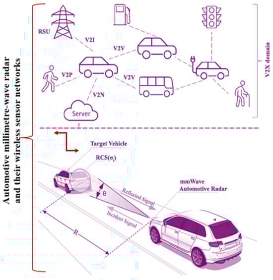
Figure 1.
Overview of an automotive radar in WSN.
Developing transceiver (TRX) circuits for this frequency range presents several challenges, including the need to design circuits that consume very little power while maintaining high integration and producing very low phase noise in the process. The voltage-controlled oscillator (VCO), one of the most important parts of a TRX, needs to fulfill these exacting performance standards.
A VCO with three critical characteristics, i.e., a large tuning range, low power consumption, and minimal phase noise, is necessitated by the demanding requirements of a 5G TRX system. With CMOS technology, VCOs can be difficult to design due to their limited transconductance, and this difficulty is compounded when designing low-power circuits operating at high frequencies, such as in the 24 GHz to 86 GHz range that is required for 5G. The challenges of circuit design have been addressed by utilizing a variety of circuit design techniques [5]. For instance, different circuit topologies and the use of a current-reuse configuration are discussed regarding the receiver design in [6] and the transceiver design in [7]. While high data transfer rates are offered by traditional VCO designs using cascoded transistor structures, high power consumption is often suffered from by them. To lessen this problem, different RF circuits, such as amplifiers [8] and VCOs [9,10], have had the current-reuse configuration applied. The block diagram of the optimization algorithm integrated with the RF circuit is shown in Figure 2.
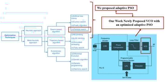
Figure 2.
Optimization algorithm integrated with an RF circuit block.
However, the use of N/PMOS cross-coupled transistors in current-reuse VCOs results in phase noise degradation and transconductance mismatch because of the phase noise degradation and transconductance mismatch that can occur. To mitigate these issues [11], the resistive degeneration approach has been used to balance transconductance and enhance the VCO’s overall performance characteristics.
Optimization algorithms are broadly used in various scientific and engineering disciplines to improve performance and fine-tune circuit designs. The complexity of designing an optimal RF system is due to the unique requirements of each system. For example, high efficiency and power are required by radar applications, whereas high linearity and wide bandwidth are demanded by base station applications [12]. The performance of a VCO is determined by its component values and transistor model, but in order to improve its characteristics, additional optimizations are often required.
Researchers have applied several optimization techniques to RF circuit design. Kouhalvandi, L. [13] and Koziel, S. [14] introduced the space mapping concept for engineering optimization, while engineers have used Bayesian optimization for RF design [15]. Modeling and designing RF systems with artificial neural networks have also become popular. Additionally, the shape-preserving response, FSRFT, Padé approximation [16], and simplified real frequency technique (SRFT) [17] are notable optimization techniques. Automated optimization techniques have also been focused on by several studies. For instance, Kouhalvandi et al. [18] utilized TSEMO, a deep learning-based approach, to optimize the number and value of passive components in circuit design. Similarly, Bayesian optimization has been used to design a high-efficiency transmitter [19,20]. However, these techniques can be complex when implemented in real-world scenarios. According to Chuan Li et al. [21], the challenges of nonlinearity in transmitters result in convergence problems that can be resolved through simulation annealing PSO analysis, which is a method of analyzing a PSO-based transmitter. In [22], Hosseini S. A. introduced how a fractional-order PSO can be used to optimize a transmitter design and achieve 26.3% efficiency at 2.4 GHz, as well as a holistic optimization strategy at 65–85 GHz that assisted in achieving 26.3% efficiency.
In this paper, an improved optimization strategy is proposed to enhance the performance of VCOs. Our approach in this paper is to introduce an adaptive scaling term into traditional particle swarm optimization (PSO) in order to improve the speed of the optimization process, as well as to simulate a stochastic simulation of the optimization process. The proposed approach is integrated into the design of a VCO, which results in fine-tuning of the component values by the adaptive PSO, which delivers faster optimization and better overall performance.
Major Contributions
In this paper, an adaptive PSO is presented to design a VCO for automotive radar systems. The major contributions of our work are listed as follows:
- In our work, we present an adaptive PSO and use it to optimize VCO circuit components.
- We make changes to the proposed algorithm for the formulation of an adaptive PSO, which helps to optimize the VCO.
- Benchmark test functions are used to justify the adaptive PSO’s performance by comparing the proposed adaptive PSO with a traditional PSO.
- A low phase noise VCO with 24 GHz operating frequency is designed in the CMOS 65-nm process.
The structure of a paper is as follows. The problem identification in the traditional PSO and proposed adaptive PSO method for VCO optimization is presented in Section 2. In Section 3, the proposed adaptive PSO algorithm is explained, along with the VCO circuit design. Results and discussion are examined in Section 4. Finally, in Section 5, the conclusions are drawn.
2. Problem Identification in PSO
Below are five key points that identify problems with the traditional PSO and how our proposed adaptive PSO addresses them:
- A traditional PSO employs a fixed velocity limit () throughout all iterations, which can lead to slow convergence. Adaptive PSOs introduce an adaptive scaling term that gradually reduces Vmax as the algorithm progresses, thereby speeding up the convergence and reducing the total number of objective function evaluations.
- In traditional PSOs, the constant search scale may initially allow for ample exploration but does not adequately shift towards exploitation (fine-tuning) in later stages. The adaptive PSO strategically decreases the search scale over time, ensuring a broad initial search for global optima and a focused, refined search as the algorithm nears convergence.
- Evaluating candidate solutions is computationally expensive; therefore, traditional PSOs may require many evaluations due to their slower convergence rate. Adaptive PSOs minimize the computational cost by reducing the number of evaluations needed, making them more efficient in scenarios where each function evaluation is resource-intensive.
- The fixed parameter settings in traditional PSOs do not adapt to different phases of the search process, potentially limiting their performance across diverse optimization problems. In contrast, adaptive PSOs incorporate a tunable scaling factor (controlled by the positive constant h) that adapts based on current generation, providing greater flexibility and robustness across various stages of the optimization process.The comparison between Traditional PSO and Proposed adaptive PSO is shown in Figure 3.
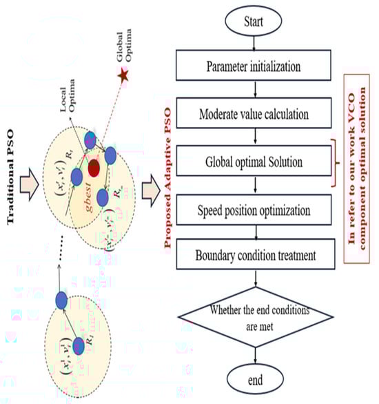 Figure 3. (left) Traditional PSO. (right) Proposed adaptive PSO.
3. The Proposed Adaptive PSO Algorithm
In our work concerning the proposed adaptive PSO, we modify the existing algorithm in the following way: in a D-dimensional space, the jth particle is denoted as . The highest fitness value is , and refers to the index of the best particle within the entire population of j particles. is the velocity (i.e., the rate of change in position) for the jth particle.
The particle adjustments in the traditional PSO are provided in (1).
In contrast, the proposed adaptive PSO algorithm modifies the velocity update rule to incorporate an adaptive scaling factor. This factor, which is gradually reduced over time, adjusts the velocity limits dynamically to speed up convergence and improve the exploration–exploitation balance. Specifically, as the algorithm progresses, the velocity limit Vmax decreases, promoting faster convergence and reducing the number of objective function evaluations required. Furthermore, the adaptive PSO algorithm incorporates a tunable scaling factor controlled by a positive constant h, which adapts based on current generation. This parameter allows the algorithm to adjust more effectively across different phases of the search process, providing greater flexibility and improving performance in diverse optimization scenarios.
In the adaptive PSO algorithm, , is a positive constant, and and are random functions whose values lie within the range of [0, 1]. Constants and are used in the algorithm, while Smax is a parameter that limits the rate of change in the particle’s position, acting as a system parameter in the PSO algorithm.
In a search method based on population, a larger search space is anticipated in the initial stages; therefore, a diverse population is beneficial to guide the system towards the global optima. As the search progresses, however, the search size is expected to decrease to refine the solution. To address this, the introduction of a multiplying factor within the traditional PSO algorithm is considered effective in accelerating convergence.
The adaptive PSO algorithm works similarly to the traditional PSO algorithm, with the addition of a multiplying factor that is incorporated to update the parameter in (2). In this multiplying factor, t is the number of generations completed so far, T is the maximum number of generations, and H is the constant term using the generate-and-test method.
The adaptive PSO algorithm, as explained in (2), evolves with a gradually shrinking search space, which facilitates more efficient convergence towards the optimal solution.
3.1. Experiments and Benchmark Test Functions
In our work, we chose three benchmark functions, as shown in Table 1.

Table 1.
Benchmark test functions.
The performance of the adaptive PSO algorithm can be significantly influenced by the Smax parameter. The value of that resulted in the best minimum for the algorithm was selected and used consistently for that specific benchmark function in subsequent experiments. Furthermore, the scaling factor “H” in the adaptive PSO algorithm was optimized through a trial-and-error process, with a constant value of H = 0.05 applied across all benchmark test functions during the experiment. For the adaptive PSO, the maximum velocity values, , used in the benchmark test function experiments for , , and were 0.25, 0.20, and 5.00, respectively. In contrast, for the traditional PSO, the values of for , , and were 0.05, 0.01, and 0.5, respectively. The convergence data for the best solutions of the three benchmark test functions averaged over 50 runs for both the traditional and adaptive PSO algorithms are shown in Figure 4, Figure 5 and Figure 6, respectively. Additionally, the averaged results from these 50 runs are presented in Table 2.
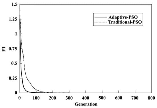
Figure 4.
Convergence of adaptive and traditional PSO algorithms for .
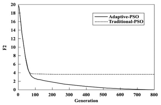
Figure 5.
Convergence records of top solutions of adaptive and traditional PSO algorithms for .
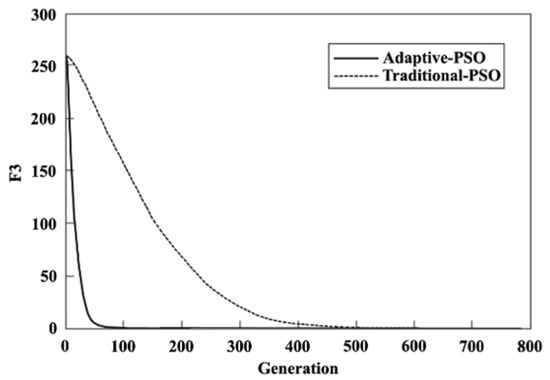
Figure 6.
Convergence records of top solutions of adaptive and traditional PSO algorithms for .
Table 2.
Statistical outcomes of the benchmark test function experiments.
According to Figure 7 and Figure 8, the average value of the best function ( & ) of the 50 running trials is shown below, compared with the parameters for the maximum value. These figures show that the best function value for the traditional PSO algorithm varies sharply with respect to , whereas for the adaptive PSO algorithm, it varies very gently with .
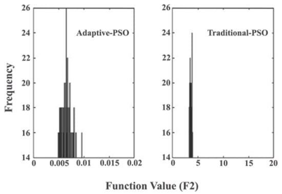
Figure 7.
Histograms of , including final values searched for by the adaptive and traditional PSO algorithms over 50 trials.
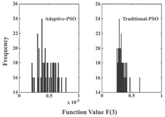
Figure 8.
Histograms of , including final values searched for by the adaptive and traditional PSO algorithms over 50 trials.
3.2. Time Complexity
In optimization algorithms, time complexity is a crucial factor that determines how efficiently an algorithm solves a problem based on the input size. Figure 9 presents a time complexity analysis comparing genetic algorithms (GA), simulated annealing (SA), and adaptive particle swarm optimization (Adaptive PSO).
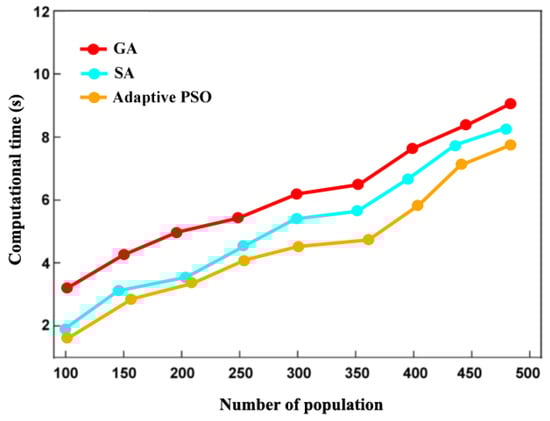
Figure 9.
Time complexity analysis between GA, SA, and the adaptive PSO algorithm.
The results indicate that the adaptive PSO exhibits lower time complexity compared to traditional GA. This advantage arises because particles in the adaptive PSO traverse the solution space more efficiently. In contrast, GA relies on crossover and mutation operations, which can increase computational complexity, particularly when dealing with large populations. The time required for VCO design using an adaptive PSO is approximately 4.1 s. In comparison, GA takes around 6.09 s, while SA requires about 5.3 s. These findings demonstrate the computational efficiency of an adaptive PSO over GA and SA.
3.3. Circuit Design
The designed VCO’s schematic is depicted in Figure 10. The proposed VCO’s LC tank circuit is composed of capacitors and and inductor . To make up for the losses of the LC tank circuit of VCO, the negative transconductance is provided by the PMOS transistor () and NMOS transistor (). These transistors ( and ), along with the LC tank circuit, formed a traditional current reuse VCO architecture.
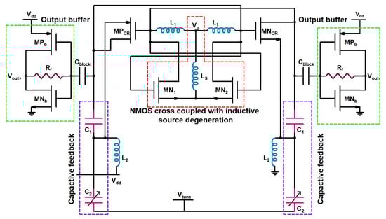
Figure 10.
Proposed VCO design and operational behavior of the VCO.
The traditional current reuse topology is selected for this VCO study because of its low power consumption. In this VCO topology, the current consumption is compared to other VCO topologies. This can be understood by the functioning of the designed VCO, which is realized with an LC tank circuit with a PMOS transistor and NMOS as a switch. The PMOS switch and NMOS switch are turned ON during the output oscillation’s positive half cycle, and during this time, the current flows supply voltages to the ground and charges the LC tank circuit of the VCO. Later, during the output oscillation’s negative half cycle, the PMOS switch and NMOS switch will be turned OFF, and VCO’s LC tank circuit discharges in this period. So, the power consumption is cut to during the positive half cycle of the output oscillations.
To further decrease the power consumption of the designed VCO, the transistor and are biased as , where VGS is the gate to source voltages and is the threshold voltage of transistors and ; this biasing configuration of the transistor is known as subthreshold biasing. In this, the VGS and drain current of the and transistors follow an exponential relation. However, the VGS and Ids of transistors exhibit a square law relation in the saturation region. The of the transistors in the subthreshold region are shown in Equation (3).
where is the thermal voltage, and n is the subthreshold slope coefficient. The magnitude of is very small, so it further reduces power consumption. In addition to power saving, the subthreshold region biasing of transistors and also has advantages in decreasing the phase noise of the VCO in the region. This is because of a small flowing current, as the MOS transistor’s thermal noise is analogous to the shot noise in the subthreshold region.
The traditional VCO current reuse topology offers many benefits of low power and low phase noise, but it suffers from low transconductance, which is inadequate for smooth oscillations, as it consists of P/NMOS transistors, which both have mismatched transconductances. To solve this issue and to have enough transconductance for smooth VCO oscillations, the designed VCO is integrated with cross-coupled NMOS transistors MN1 and MN2. This inclusion of NMOS transistor pairs helps to provide the required transconductance, but it also contributes to increasing the phase noise of VCO, so to eliminate this phase noise contribution in designed VCO, a source inductive degeneration technique is implemented by using inductor . The oscillation condition for the startup of the proposed VCO must satisfy Equation (4).
where , , and are the parasitic resistance of inductors , , and . Zin1 is the input impedance of transistors and , which is provided by Equation (5), and Zin2 is the input impedance of transistor , which is provided by Equation (6).
where , , and are transconductances of , , and , respectively. Analyzing the small signal closed loop voltage gain (Vo/Vi) of the proposed VCO, the voltage gain Vo/Vi = 1 at any oscillating frequency is provided by Equation (7), and the oscillation frequency is shown in Equation (8).
For a simple phase noise analysis of the proposed VCO, the gate noises of , , , and are illustrated by . The thermal noise and low frequency 1/f noise of transistors , , , and are represented by , , , and , respectively. The LC tank thermal noise is represented by . For phase noise computations of the VCO, the channel thermal noise, power densities of transistor gate noise, 1/f noise [11], and LC tank thermal noise are shown in Equations (9), (10) and (11), respectively. The total phase noise of the VCO is also defined in Equation (12).
where is the power of a VCO oscillating signal, and is the spectral power density of the VCO noise. It is depicted in Equation (12) that the higher the VCO output signal, the lower the VCO phase noise.
Figure 11 illustrates the flow chart of an optimized VCO. Adaptive PSO parameters such as the initial population size, initial position of the particle, and rate of change in position (velocity) of particles are determined using the Agilent ADS software’s PSO optimization tool (v. 2022). As a result, for each optimization cycle, random generation is conducted due to the initial size of the population.
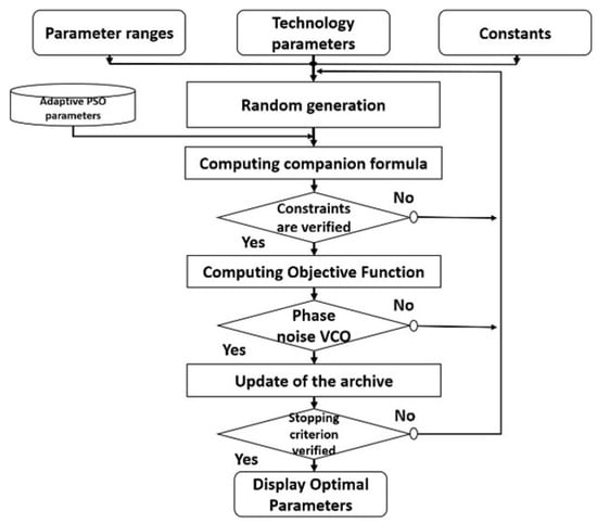
Figure 11.
Optimized VCO flowchart using an adaptive PSO.
In our work, we focus our attention on phase noise, which is the most important performance parameter of VCOs. In our study, MATLAB (v.2017) and ADS keysight ADS 2022 are the software used. In the ADS software, there is a MATLAB co-simulation window that utilizes MATLAB to integrate the AD with MATLAB. Then, the ADS RF window is applied with the designed VCO and the MATLAB script with ADS. Within the MATLAB environment, adaptive PSO coding is assigned and named by separate blocks of code. During the adaptive PSO’s optimization process, the phase noise’s numerical value is determined by utilizing the VCO block. In the MATLAB block, all the parameters of the adaptive PSO and variables of the VCO design are initialized. In the first step, all the variables of the design are randomly created from the intended block of MATLAB. Then, a text file is saved. The first set of design variables is given to the designed VCO in the form of an ADS text file. The designed VCO sets its output, i.e., phase noise value, as the input of the second MATLAB link. First, we assign the best and worst values, respectively. Then, in the second step, the VCO is joined to the other set of design variables. Its phase noise value is computed and compared with the best value. Until we find the best solution, we continue the loop of the algorithm. Iterations of this algorithm continue until the maximum number is reached. Finally, it is possible to achieve the desired phase noise. Table 3 shows that by using the adaptive PSO, we are able to obtain optimal design variables of the VCO. The circuit element dimensions of the proposed VCO are determined in Table 3.
Table 3.
Optimized VCO circuit element dimensions.
4. Result and Discussion
Figure 12 and Figure 13 show the comparison of the simulated phase noise of the designed VCO using GA and SA and by using the adaptive PSO algorithm and without the adaptive PSO algorithm, respectively. In Figure 12, at 1 MHz frequency offset, we can see the VCO phase noise performance using GA and SA. The phase noise of the VCO using GA is −118.5 dBc/Hz. Meanwhile, for SA, it is −116.9 dBc/Hz. In Figure 13, at 1 MHz frequency offset, we can see that the adaptive PSO outperformed the VCO without the adaptive PSO algorithm with almost −4.7 dbc/Hz enhancement in the phase noise value. The phase noise of the VCO with the adaptive PSO algorithm is −120 dBc/Hz @ 1 MHz and −140 dBc/Hz @ 10 MHz. The phase noise of VCO without an algorithm is −115.3 dBc/Hz @ 1 MHz and 135.3 dBc/Hz @ 10 MHz.
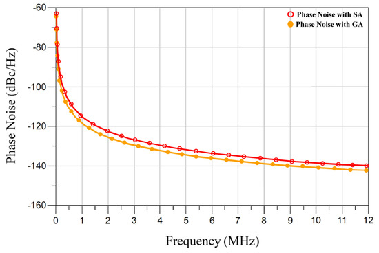
Figure 12.
VCO phase noise performance using GA and SA.
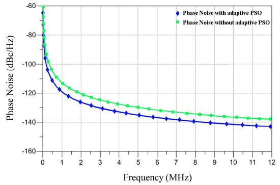
Figure 13.
VCO phase noise performance with and without an adaptive PSO.
Figure 14 shows the complete phase noise profile of the optimized VCO with respect to the tuning voltage of varactors that range from 0 V to 1 V. By setting the proper tunning voltages of the varactors, the optimized phase noise of the designed VCO can be achieved with different oscillating frequencies.
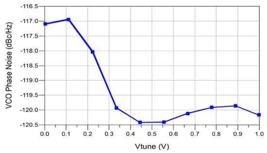
Figure 14.
VCO phase noise performance versus tuning voltage.
The optimized VCO oscillating frequency range with respect to the tuning voltage of varactors, which ranges from 0 V to 1 V, is illustrated in Figure 15. The optimized VCO with an adaptive PSO oscillates with a frequency range of 21.2%, and the center oscillation frequency of the optimized VCO is 24.2 GHz. The wide frequency range of an optimized VCO is achieved with the aid of C2 varactors that form a parallel connection with the source terminal of transistors and .
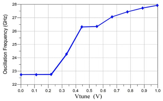
Figure 15.
Frequency range of the optimized VCO.
The transient response of the optimized VCO provides symmetrical and differential waveforms, such as Vout+ and Vout−, which are depicted in Figure 16.
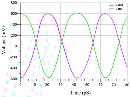
Figure 16.
Output signal waveforms of the designed VCO.
The designed VCO is simulated under different processes, environments, and state conditions to verify the VCO operation under different PVT conditions. The Monte Carlo simulation with three different semiconductor process corners, defined as follows, is used to verify the stable operability of VCO:
Best case: (FF) corner process (0.45 V, −55 °C);
Typical case: TT corner process (0.4 V, 27 °C);
Worst case: SS corner process (0.35 V, 125 °C).
The variations of phase noise of the designed VCO with respect to PVT are simulated using the Monte Carlo simulation. Histograms of the phase noise are shown in Figure 17 below. The mean value of phase noise is -120.06 dBc/Hz, and its standard deviation is 1.47%.
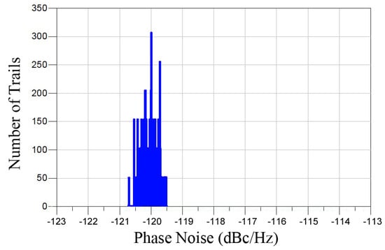
Figure 17.
Phase noise histogram.
The simulation results with respect to PVT variation at semiconductor process corners are shown in Table 4. The VCO oscillates in all three studied corners. In the FF corner, power consumption and frequency drift by 11.5% and 0.1%, respectively, compared to the TT corner. In the SS corner, power consumption and frequency drift by 12.6% and 0.41%, respectively, compared to the TT corner.
Table 4.
PVT variation simulation results.
The performance parameter comparison of the adaptive PSO-based optimized VCO with [23,24,25,26,27,28] state-of-the-art published work is provided in Table 5. Table 5 depicts the better performance of the designed VCO over other published works from the perspective of performance parameters like phase noise, which is −120 dBc/Hz @ 1 MHz offset, and oscillating frequency range, which is 21.2%.
Table 5.
Performance summary of state-of-the-art VCOs.
5. Conclusions
This paper presented an adaptive PSO approach for optimizing a 24 GHz VCO in next-generation wireless sensor networks, particularly for self-driving vehicle radar systems. The proposed adaptive PSO algorithm enhances the optimization process by reducing the number of calculations while improving efficiency in complex engineering problems. The performance evaluation using benchmark functions demonstrated the effectiveness of the adaptive PSO in achieving faster convergence and better optimization results. The VCO using an adaptive PSO resulted in significant improvements, achieving a low phase noise of −120 dBc/Hz at a 1 MHz offset, a wide tuning range of 21.2%, and ultra-low-power consumption of only 1.35 mW at 0.9 V. In our work, a comparative analysis with traditional PSO techniques further validated the superiority of the proposed method in optimizing the VCO for automotive radar applications. The results show that adaptive PSO-based optimization is an effective method for improving the performance of radar systems in self-driving vehicles. Future work may explore extending this method to other RF circuit designs to further optimize next-generation wireless communication systems. Additionally, integrating machine learning techniques with an adaptive PSO could further improve optimization efficiency by dynamically adjusting algorithm parameters based on real-time feedback. Finally, exploring the potential of this optimization approach in emerging technologies, such as 6G communication systems and Internet of Things (IoT) applications, could pave the way for more efficient and scalable RF circuit designs.
Author Contributions
Conceptualization, K.T., U.A. and T.S.D.; methodology, K.T., U.A., T.S.D. and Y.L.; validation, M.N.A., J.-Y.R. and B.-S.K.; formal analysis, K.T., U.A. and T.S.D.; investigation, K.T. and U.A.; resources, Y.L., J.-Y.R. and B.-S.K.; writing—original draft preparation, K.T., U.A. and T.S.D.; writing—review editing, M.N.A., Y.L., J.-Y.R. and B.-S.K.; supervision, Y.L., J.-Y.R. and B.-S.K.; funding acquisition, Y.L., J.-Y.R. and B.-S.K. All authors have read and agreed to the published version of the manuscript.
Funding
The authors acknowledge funding from the National Research Foundation (NRF) of Korea through the BK21 FOUR Project (Smart Robot Convergence and Application Education Research Center) (Grant Number: 2018R1D1A1B07043286).
Institutional Review Board Statement
Not applicable.
Informed Consent Statement
Not applicable.
Data Availability Statement
Data are contained within the article.
Conflicts of Interest
The authors declare no conflicts of interest.
References
- Yeh, C.; Chang, K.; Ko, Y.; Kim, I. ITU-R Activities for Standardization of 6G Technologies. Electron. Telecommun. Trends 2024, 39, 87–97. [Google Scholar]
- Mahapatra, R.K.; Kaliyath, Y.; Shet, N.; Mahapatro, S.R.; Satapathi, G.S.; Prusty, S.B.; Patro, B.S. A survey on wireless sensor network (applications and architecture). Int. J. Commun. Netw. Distrib. Syst. 2024, 30, 136–201. [Google Scholar]
- You, T.; Jin, H.; Li, P. Optimal placement of wireless sensor nodes for bridge dynamic monitoring based on improved particle swarm algorithm. Int. J. Distrib. Sens. Netw. 2013, 9, 390936. [Google Scholar]
- Sahoo, S.S.; Mohanty, S.; Sahoo, K.S.; Daneshmand, M.; Gandomi, A.H. A Three-Factor-Based Authentication Scheme of 5G Wireless Sensor Networks for IoT System. IEEE Internet Things J. 2023, 10, 15087–15099. [Google Scholar] [CrossRef]
- Jamshed, M.A.; Ali, K.; Abbasi, Q.H.; Imran, M.A.; Ur-Rehman, M. Challenges, applications, and future of wireless sensors in Internet of Things: A review. IEEE Sens. J. 2022, 22, 5482–5494. [Google Scholar]
- Park, B.; Kwon, K. 2.4 GHz BLE receiver with power-efficient quadrature RF-to-baseband-current-reuse architecture for low-power IoT applications. IEEE Access 2021, 9, 62734–62744. [Google Scholar] [CrossRef]
- Kim, S.J.; Park, C.S.; Lee, S.G. A 2.4-GHz Ternary Sequence Spread Spectrum OOK Transceiver for Reliable and Ultra-Low Power Sensor Network Applications. IEEE Trans. Circuits Syst. I Regul. Pap. 2017, 64, 2976–2987. [Google Scholar] [CrossRef]
- Bozorg, A.; Staszewski, R.B. A 0.02–4.5-GHz LN(T)A in 28-nm CMOS for 5G Exploiting Noise Reduction and Current Reuse. IEEE J. Solid-State Circuits 2021, 56, 404–415. [Google Scholar] [CrossRef]
- Lin, Z.; Jia, H.; Ma, R.; Deng, W.; Wang, Z.; Chi, B. A low-phase-noise VCO with common-mode resonance expansion and intrinsic differential 2nd-harmonic output based on a single three-coil transformer. IEEE J. Solid-State Circuits 2023, 59, 253–267. [Google Scholar] [CrossRef]
- Kumar, D.; Shrimali, H.; Nallam, N. A Low-Power Quadrature LC-Oscillator Using Core-and-Coupling Current-Reuse. In Proceedings of the 2021 IEEE International Symposium on Circuits and Systems (ISCAS), Virtual, 23–28 May 2021; IEEE: New York, NY, USA, 2021; pp. 1–5. [Google Scholar]
- Nguyen, D.; Ko, Y.H.; Yun, S.J.; Han, S.K.; Lee, S.G. Low phase noise LC-VCO with active source degeneration. JSTS J. Semicond. Technol. Sci. 2013, 13, 207–212. [Google Scholar]
- Chen, H.; Abbas, R.; Cheng, P.; Shirvanimoghaddam, M.; Hardjawana, W.; Bao, W.; Li, Y.; Vucetic, B. Ultra-reliable low latency cellular networks: Use cases, challenges and approaches. IEEE Commun. Mag. 2018, 56, 119–125. [Google Scholar]
- Kouhalvandi, L.; Ceylan, O.; Ozoguz, S. Optimization techniques for analog and RF circuit designs: An overview. Analog Integr. Circuits Signal Process. 2021, 106, 511–524. [Google Scholar] [CrossRef]
- Koziel, S.; Bandler, J.; Madsen, K. A Space-Mapping Framework for Engineering Optimization—Theory and Implementation. IEEE Trans. Microw. Theory Tech. 2006, 54, 3721–3730. [Google Scholar] [CrossRef]
- Huang, J.; Tao, C.; Yang, F.; Yan, C.; Zhou, D.; Zeng, X. Bayesian Optimization Approach for RF Circuit Synthesis via Multitask Neural Network Enhanced Gaussian Process. IEEE Trans. Microw. Theory Tech. 2022, 70, 4787–4795. [Google Scholar] [CrossRef]
- Wilson, C.; Zhu, A.; Cai, J.; King, J.B. Pade-Approximation Based Behavioral Modeling for RF Power Amplifier Design. IEEE Access 2021, 9, 18904–18914. [Google Scholar] [CrossRef]
- Kilinc, S.; Ormanci, M.A.; Yildirim, A.; Kizilbey, O.; Yarman, B.S. An SRFT Tool to Design Broadband Microwave Amplifiers for Complex Impedance Conditions. In Proceedings of the 2024 IEEE INC-USNC-URSI Radio Science Meeting (Joint with AP-S Symposium), Florence, Italy, 14–19 July 2024; IEEE: New York, NY, USA, 2024; pp. 99–100. [Google Scholar]
- Kouhalvandi, L. A Prospective Look on Optimization Methods For RFID Systems: Requirements, Challenges and Implementation Aspects. Balk. J. Electr. Comput. Eng. 2022, 10, 156–169. [Google Scholar] [CrossRef]
- Sena, M.; Erkilinc, M.S.; Dippon, T.; Shariati, B.; Emmerich, R.; Fischer, J.K.; Freund, R. Bayesian optimization for nonlinear system identification and pre-distortion in cognitive transmitters. J. Light. Technol. 2021, 39, 5008–5020. [Google Scholar] [CrossRef]
- Huang, J.; Fan, Z.; Cai, J. Design of A High Efficiency Sequential Load Modulated Balanced Amplifier Based on Multiple Multi-Objective Bayesian Optimization. IEEE Trans. Comput.-Aided Des. Integr. Circuits Syst. 2024, 43, 4348–4360. [Google Scholar]
- Li, C.; You, F.; Yao, T.; Wang, J.; Shi, W.; Peng, J.; He, S. Simulated annealing particle swarm optimization for high-efficiency power amplifier design. IEEE Trans. Microw. Theory Tech. 2021, 69, 2494–2505. [Google Scholar] [CrossRef]
- Hosseini, S.A.; Hajipour, A.; Tavakoli, H. Design and optimization of a CMOS power amplifier using innovative fractional-order particle swarm optimization. Appl. Soft Comput. 2019, 85, 105831. [Google Scholar] [CrossRef]
- Rout, P.K.; Acharya, D.P.; Panda, G. A multiobjective optimization based fast and robust design methodology for low power and low phase noise current starved VCO. IEEE Trans. Semicond. Manuf. 2013, 27, 43–50. [Google Scholar] [CrossRef]
- Song, J.H.; Kim, B.S.; Nam, S. A 24 GHz PMOS body voltage controlled oscillator with transformer coupled varactor. In Proceedings of the 2014 International SoC Design Conference (ISOCC), Jeju, Republic of Korea, 16–19 November 2014; IEEE: New York, NY, USA, 2014; pp. 208–209. [Google Scholar]
- Oh, J.; So, C.; Hong, S. 24 GHz phase-tunable resistively-coupled VCO. In Proceedings of the 2016 IEEE International Symposium on Radio-Frequency Integration Technology (RFIT), Kyoto, Japan, 12–14 September 2016; IEEE: New York, NY, USA, 2016; pp. 1–3. [Google Scholar]
- Krout, I.; Mnif, H.; Fakhfakh, M.; Loulou, M. Optimizing LC VCO performances through a heuristic. WSEAS Trans. Electron. 2008, 5, 274–281. [Google Scholar]
- Ebrahimi, E.; Naseh, S. Investigating the performance of cross-coupled CMOS LC-VCOs using genetic algorithm. In Proceedings of the 21st International Conference Radioelektronika 2011, Brno, Czech Republic, 27–28 April 2011; IEEE: New York, NY, USA, 2011; pp. 1–4. [Google Scholar]
- Yang, J.; Kim, C.Y.; Kim, D.W.; Hong, S. Design of a 24-GHz CMOS VCO with an asymmetric-width transformer. IEEE Trans. Circuits Syst. II Express Briefs 2010, 57, 173–177. [Google Scholar]
Disclaimer/Publisher’s Note: The statements, opinions and data contained in all publications are solely those of the individual author(s) and contributor(s) and not of MDPI and/or the editor(s). MDPI and/or the editor(s) disclaim responsibility for any injury to people or property resulting from any ideas, methods, instructions or products referred to in the content. |
© 2025 by the authors. Licensee MDPI, Basel, Switzerland. This article is an open access article distributed under the terms and conditions of the Creative Commons Attribution (CC BY) license (https://creativecommons.org/licenses/by/4.0/).