1. Introduction
The increasing global demand for energy, beside the depletion of fossil fuel stocks and their irrational use, has led to severe negative effects on the environment, including accelerated global warming. Faced with these challenges, researchers have been actively exploring sustainable solutions [
1,
2]. Indeed, renewable energy sources, especially solar energy based on solar cells, have gained significant attention from researchers in the last decades as viable alternatives to the conventional resources of energy. However, enhancing the energy conversion efficiency of solar cells remains a critical challenge for ensuring the optimal performance of these devices. Over time, advances in materials and multi-junction structures, such as indium gallium phosphide (InGaP) and gallium arsenide (GaAs), have played a key role in enhancing solar cell performance. However, the rapid technological progress during recent years, driven by cost reductions and efficiency improvements, has also led to significant advancements in the manufacturing of multi-junction monolithic solar cells based on III–V semiconductor materials.
During the last years, experimental investigations on InGaP/GaAs dual-junction solar cells (DJSCs) revealed substantial efficiency gains, where the National Renewable Energy Laboratory (NREL) achieved an efficiency of 32.8% [
3]. In the same context, the study presented by Singh Khomdram Jolson and Subir Kumar Sarkar in [
4] succeeded in achieving an efficiency of 32.1964% (1 sun) and 36.6781% (1000 suns) in a double-junction InGaP/GaAs solar cell using a BSF InAlGaP layer. Similarly, in [
5], Bagheri Shadi et al. experimentally achieved the efficiency of 36.24% by dividing the tunnel zone into six layers on the InGaP/GaAs solar cell. Whereas the highest reported efficiency to date is 40.879%, which is obtained in [
6] by Dutta J.P. et al. through an optimized tandem junction InGaP/GaAs solar cell with a double top back surface field (BSF), where it was proved that the InGaP tunnel junction layer demonstrates high conversion efficiency. Further contributions include the study by Smriti Baruah et al. [
7] and Nayak P. P. et al. [
8], which explored different solar cell configurations and enhancements in double-junction InGaP/GaAs solar cells, incorporating innovations like carbon nanotubes. Other studies were carried out to improve the performance of the aforementioned solar cell, especially on a double-junction structure, such as in [
1], Abdelbasset Bakour et al. introduced a layer of ZnO to optimize GaInP/GaAs tandem solar cells, where the author achieved an efficiency improvement of 5.52%. In [
9], Djaafar F. et al. developed optimal model variables for InGaP/GaAs solar cells to increase the efficiency, while in [
10], Bennett Widyolar et al. proposed a modeling approach for double-junction InGaP/GaAs solar cells. In [
11], Fatima Zahra Kharchich and Abdellatif Khamlichi proposed an InGaP/GaAs double-junction structure, leveraging 2D codes through Silvaco-Atlas software for optimal design.
Further research was presented to improve the multi-junction InGaP/GaAs/InGaAsP/InGaAs solar cells, such as the study published in [
12] by Gyujin Oh et al., where the anti-reflective coating layer is used to increase the efficiency. In [
13], Duy Phong Pham et al. optimized four-terminal GaAs/Si tandem solar cells by testing various anti-reflection layers, showcasing technological maturity. In [
14], Kuan W. A. Chee and Yuning Hu focused on the optimal shape of InGaP/GaAs solar cells to enhance energy conversion efficiency. In [
15], Hamidreza Arzbin and Abbas Ghadimi developed a reliable model for InGaP/GaAs DJSCs, which was validated through comparison with other structures. In [
16], Sukeerthi M. and Siva Kotamraju studied the degradation effects on solar cells by examining the triple-junction type-InGaP/InGaAs-GaAsP MQW/InGaAs in the aim to maximize the efficiency. In [
17], Tomah Sogabe et al. characterized the effects of fluctuations in the InAs/GaAs solar cell intermediate band to ensure the maximized efficiency and the stability in organometallic solar cells.
It is worthy to clarify that III–V semiconductors play a crucial role in advancing solar cell technology due to their exceptional optoelectronic properties. It is well known that these materials exhibit high absorption coefficients, direct bandgaps, and superior carrier mobility, making them ideal for high-efficiency multi-junction solar cells. The continuous improvement in III–V semiconductor processing has demonstrated a record-breaking efficiency in multi-junction solar cells, reinforcing their importance in the future of photovoltaic energy. In [
18], Vashishtha et al. developed a self-powered GaN-nanowall-network photodetector with bidirectional photocurrent generation, achieving responsivities of −2.5 A W
−1 (266 nm) and 1.7 A W
−1 (355 nm) [
18]. The same authors proved in [
19] that the GaN hexagonal nano-spike photodetector further exhibited high sensitivity, reaching 2100 mA W
−1 responsivity under solar-blind UV light, highlighting its potential for self-powered optoelectronics. Advancements in heterostructure engineering emphasize the synergy between III–V materials, and emerging semiconductors were presented in some research studies, such as in [
20], where Vashishtha et al. integrated monolayer MoS₂ with GaN to develop a self-powered, bidirectional photodetector with a responsivity of 631 mA W
−1 at 0 V bias, operating across UV and visible spectra. This heterostructure leverages the strengths of 2D materials and III–V compounds, similar to tandem solar cell designs. Additionally, the Sb
2Se
3/GaN heterojunction achieved ultra-high responsivity and maintained thermal stability up to 250 °C, demonstrating the robustness of III–V-based systems under extreme constraints [
21].
This study focuses on the development of an InGaP/GaAs double-junction solar cell (DJSC) structure, integrating a buffer layer in the lower junction and a new back surface field (BSF) in the upper junction. The design was optimized using the Silvaco ATLAS simulator under the AM1.5G standard spectrum. It is found that by systematically adjusting the layer thickness, buffer layer carrier concentration, and BSF properties, the solar cell’s performance was significantly enhanced compared to the baseline. Furthermore, the impact of operating temperature on key performance metrics was analyzed, and it was found that it can offer valuable insights for improving efficiency and reliability in advanced photovoltaic technologies.
2. Modeling of InGaP/GaAs Tandem Solar Cells
2.1. Studied InGaP/GaAs Structure
This section explores the modeling of InGaP/GaAs tandem photovoltaic solar cells in the main aim to establish the foundation for a novel multi-junction system based on these absorber materials. To ensure an accurate presentation of the proposed structure, this study begins with an in-depth presentation of the cell structure, followed by a detailed examination of the used physical models.
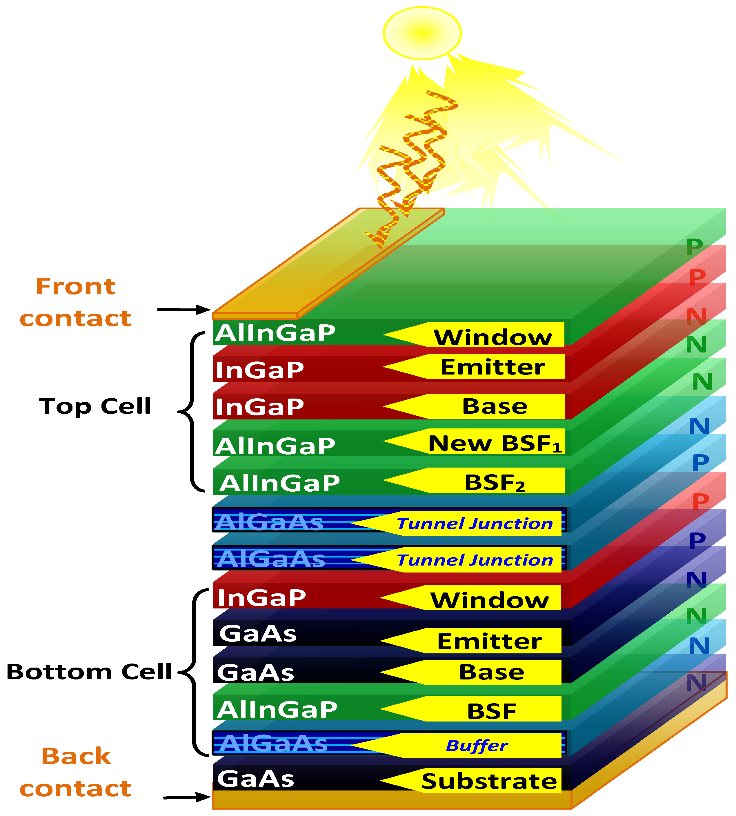
The studied InGaP/GaAs tandem solar cell in this paper, depicted in
Figure 1, emerges as a promising candidate, boasting a double-junction architecture. This intriguing structure features an upper cell crafted from InGaP (
Eg = 1.9 eV) and a lower cell composed of GaAs (
Eg = 1.42 eV). These cells are intricately intertwined through an AlGaAs/AlGaAs tunnel junction, enabling both electrical and optical connection.
This solar cell is composed of an upper InGaP cell, which leverages a p-n junction serving as both emitter and base, with AlInGaP acting as the window layer. This ingenious design mitigates thermalization losses inherent to low-gap materials and transmission losses associated with large-gap materials, paving the way for enhanced efficiency. Furthermore, an additional back surface field (BSF) layer is strategically positioned for further performance optimization. However, the bottom cell, a GaAs cell, contains a p-n junction functioning as the emitter/base, accompanied by a p+-type InGaP window layer and an n-type AlInGaP BSF layer. Whereas the inclusion of the tunnel junction composed of the AlGaAs buffer layer beneath these two cells plays a crucial role in boosting overall efficiency.
Table 1 offers a detailed breakdown of the material composition, thicknesses, and doping concentrations for each region within the studied structures. It is worth noting that gold contacts are employed in the front and back layers to amplify absorption. These meticulously characterized material properties serve as the foundation for developing the geometry of each section in the proposed structure, providing the basis for modeling and configuring the InGaP/GaAs tandem solar cells.
Table 2 provides a critical reference point, summarizing the key characteristics of each material used in the design of the studied InGaP/GaAs tandem solar cell.
2.2. Physical Models
It is obvious that the accurate modeling of the tunnel junction within a solar cell’s structure plays a crucial role in understanding and optimizing its performance. This complex and challenging task is addressed using the nonlocal band-to-band tunneling (NLBBT) model. Indeed, an electrode is introduced, which is seamlessly adapted to the interlayer’s geometry, coupled with an overall resistor. This resistor allows ensuring precise current flow from the anode to the cathode, preventing unwanted leakage through the introduced electrode [
24,
25,
26,
27,
28].
The physical model of the studied solar cell in this paper is implemented in Silvaco’s ATLAS TCAD, which is an advanced computer-aided design (CAD) software (version 2018) that was proved for its capability to accurately simulate semiconductor device behavior [
29,
30,
31]. This powerful tool integrates a range of models, including Fermi level, concentration-dependent mobility (CONMOB), Shockley-Read-Hall (SRH) recombination, optical recombination (OPTR), band-gap narrowing (BGN), and Auger recombination, enabling precise replication of the intricate physical mechanisms governing solar cell performance under various operating conditions [
32,
33,
34].
2.3. Recombination Model
Semiconductor imperfections, such as impurities and defects, introduce trapping levels that impact charge carrier lifetimes and recombination processes. Indeed, the Shockley-Read-Hall (SRH) model in semiconductors describes how electrons are trapped by defect states and subsequently recombine with holes in the valence band, leading to the decrease in the number of free charge carriers. This versatile model accounts for recombination in different regions of the device, taking into account factors such as trap density and energy levels, making it essential for optimizing semiconductor and photonic devices.
This model takes into consideration the dynamics of electrons during their interactions with trapping sites acting as donors and acceptors within the device. To integrate this model, simply activate the SRH parameter in the MODELS instruction of the ATLAS code. The formulation of the SRH model is expressed as follows [
35]:
In the context of this model, the symbols “” and “” represent the concentrations of electrons and holes, respectively. The term “” denotes the “intrinsic carrier concentration”, while “” signifies the gap between the trap energy level and the intrinsic Fermi level. Additionally, “” corresponds to the lattice temperature measured in degrees Kelvin.
Furthermore, “
” and “
” represent the lifetimes of electrons and holes, respectively. It is crucial to note that the values of “
” and “
” are contingent on the type of trap and the volume density of trapping
effects. It should be emphasized that users have the flexibility to customize these electron and whole lifetime parameters, “
” and “
”, using the MATERIAL instruction [
12]. These parameters play a pivotal role in characterizing the dynamic behavior of the semiconductor, offering a nuanced understanding of carrier concentrations, intrinsic properties, and thermal effects within the material.
2.4. Electrical Characteristics
Analyzing the fundamental electrical properties of a solar cell is an essential method for evaluating its performance. During the process of optimizing a specific design, considering these parameters proves to be the crucial first step. The main electrical characteristics on which this study is focused are the short-circuit current density
, the conversion efficiency
, the filling factor
, and the open circuit voltage
. Their definition is based on the main known variables such as [
9,
31] the current generated by the light or the photo-generated current
, the dark current or reverse saturation current
, the Boltzmann constant
, the ideality factor of the diode
, the temperature of the cells
(K), the elementary charge
,
the maximum power
, and the incident power
. The current in the solar cell is defined as follows [
29]:
The open circuit voltage
is expressed as follows [
29]:
And the fill factor
equation is given as follows [
29]:
The maximum power conversion
, which can be achieved by transforming solar energy coming from the solar spectrum into electricity, can be expressed as follows [
29]:
Hence, the conversion efficiency can be calculated as follows [
29]:
These equations provide a solid theoretical basis for in-depth analysis of the electrical performance of a solar cell, thereby effectively guiding the optimization process of double-junction solar cell design.
3. Results and Discussions
In this study, the optimal double-junction cell design is investigated to obtain higher solar cell efficiency. Indeed, this study focuses mainly on the optimization of the solar cell structure presented in
Figure 1, which is based on the incorporation of a buffer layer and a double back surface field (BSF) layer, with the main goal of enhancing its performance, mainly the efficiency.
The methodology used in this investigation systematically characterizes the properties of and that allow establishing a foundation for optimizing their respective single-junction cells. Whereas the modeling process focuses on assessing the impact of different BSF configurations, the lattice mismatches in structures are taken into account by the integration of variable pad thicknesses. To achieve accurate design optimization through the used software, the doping concentrations and BSF layer thickness of the double-junction cell are carefully adjusted. This meticulous optimization process unveils the advantages of the main idea proposed in this study, which allows for the performance of a robust tool for designing high-efficiency tandem solar cells. The key to this performance boost lies in the synergistic interplay between the buffer layer and the upper double-layer BSF.
3.1. GaInP Single Junction Solar Cell with Double Back Surface Field
In general, III–V composite materials are found to be the most suitable for optoelectronic devices that have been extensively studied in several previous research experiments [
2,
17], allowing the achievement of optimal efficiency of multi-junction solar cells.
Figure 2 illustrates the optimized BSF layer with a double back surface field integrated into the p+/n+ type
single junction solar cell. The use of
-based pn-junction solar cells (with a bandgap energy of
Eg = 1.9 eV) represents a promising choice for ensuring thermal stability in the top cell of a double or dual-junction solar cell (DJSC).
As shown in
Figure 2, there are two types of composite materials, such as the one based on (
), which is called ternary type, and the one based on (
), which is called quaternary type. Indeed, the lattice constant (
) for both types can be calculated using Vegard’s law, which approximates the lattice constant of an alloy as a weighted average of its components. The quaternary compound
is calculated using Vegard’s law, which approximates the lattice constant of an alloy as a weighted average of its constituent binaries:
For ternary-type composed by (
), it is presented by the composition
; hence, based on Vegard’s law, the lattice constant can be calculated from the following equation:
For ternary-type composed by (
), it is presented by the composition
; hence, based on Vegard’s law, the lattice constant can be calculated from the following equation:
The lattice constant for the quaternary type composed by (
and which is presented by
can be calculated based on Vegard’s law from the following equation:
where
and
are molar fractions defining the composition of each component and shown in their presentation.
Similarly, the refractive index () of such compound materials can be modeled as a weighted sum of the refractive indices of the corresponding components, following the same compositional dependence.
In this study, the quaternary compound material (
) is introduced as a double or dual-back surface field (BSF) layer into the single-junction solar cell compound (
). It is important to mention that the BSF layer’s lattice constant must align with the substrate and adjacent layers to balance electrical performance (carrier confinement) and structural quality (defect suppression). This synergy is critical for achieving reliable, high-efficiency tandem solar cells. In
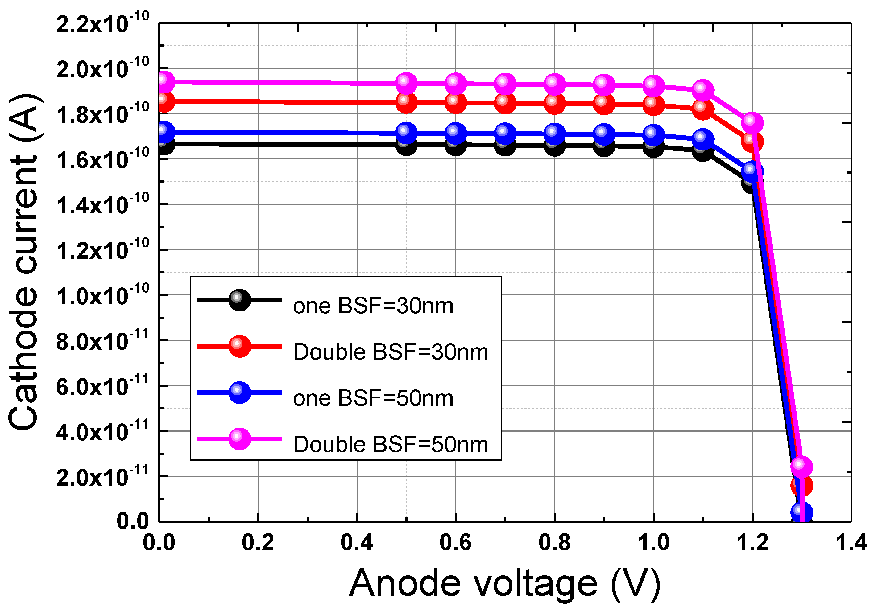
Figure 3, the short circuit current density as a function of open circuit voltage (
) is observed for two different single and double or dual-back surface field (BSF) thicknesses in the buffer. It can be noted clearly that for thicknesses of 50 µm, the cathode current densities (
) versus the slight increase in the anode voltage exhibit higher values for both single and double back surface field (BSF) compared to those of 30 µm thickness, where the optimal values for the current density and conversion efficiency obtained at short circuit are 17.170 mA/cm
2 and 18.540% and 19.384 mA/cm
2 and 21.088% for single and double BSF, respectively.
It is worthy to note that increasing the thickness of the BSF layer presents significant advantages for the enhancement of the solar cell performance, which can be ensured by improving the transport of photo-generated carriers and reducing the recombination losses at the rear surface. This improvement in carrier transport primarily results from the reduction in recombination losses, which is effectively compensated by an increased concentration of minority carriers at the rear junction. Indeed, a higher doping concentration strengthens the BSF layer, effectively repelling minority carriers from the rear contact, thereby minimizing recombination. When optimized, these factors significantly contribute to an overall improvement in solar cell performance.
The maximum efficiency is achieved with a BSF double-layer thickness of 50 nm, as shown in
Table 3.
3.2. GaAs Single Junction Solar Cell with Variable Pad Thickness
This study aims to enhance solar cell efficiency by leveraging the similar characteristics of
and the materials used in this design. Consequently,
is incorporated as a buffer layer in the
single-junction structure, as illustrated in
Figure 4. Further, the optimization of this layer is also an essential task to be ensured to achieve greater efficiency.
In this paper, the thickness of the
single-junction with double BSF layer structure was optimized in a range from 10 nm to 50 nm, while maintaining a constant doping concentration of 5 × 10
−18 cm
−3 in order to study its impact on the cell performance. The dominant parameters related to solar cells, with respect to
layer thickness, are listed in
Table 4.
Figure 5 illustrates the variations of short-circuit current (
), open-circuit voltage (
), and efficiency (
) as a function of the thickness of the
layer.
These parameters show substantial improvements as the thickness of the buffer layer increases, reaching their optimum around 50 nm. The presence of this buffer layer facilitates the efficient transport of photo-generated carriers across the junction, thus leading to a reduction in recombination losses and an accumulation of excess minority carriers at the junction. These combined effects contribute significantly to the overall improvement in the solar cell performance.
Figure 6 shows that the current density is higher for the solar cell with a layer (
) than for the solar cell with a layer (
). This is due to the fact that the (
) layer is thicker and therefore contains more free electrons. Specifically, the current density for the solar cell with a 50 nm n-layer is about 33.278 mA/cm
2, while the current density for the solar cell with a 10 nm n-layer is about 29.821 mA/cm
2. This represents an increase in the efficiency of approximately 11.6%.
3.3. Optimization of the DJSCs with Buffer and New Top BSF Layers
The configuration of the
DJSCs, generated by Silvaco-Atlas, is shown in
Figure 6.
3.3.1. Doping Optimization for AlGaAs Bottom Buffer Layer in an InGaP/GaAs DJSCs
Doping concentration plays a crucial role in modeling the configuration of a solar cell, exerting a direct influence on the extent of the depletion region. To clarify the impact of doping concentration on solar cell performance based on the approach investigated in this paper, the optimal thickness of the buffer layer is kept below 50 nm.
A comprehensive overview of solar cell parameters is available in
Table 5, covering various doping concentrations in the lower buffer layer, ranging from 1 × 10
17 to 1 × 10
20 . It can be seen that the open circuit voltage (
) increases with the increase in the doping concentration. This is due to the increased built-in potential across the junction.
The optimal doping density for achieving maximum efficiency is determined to be 1
, yielding a conversion efficiency of 33.451%. Whereas the corresponding
and
are
and
, respectively. This balance between
improvement and the stability of
highlights the importance of optimizing the doping concentration to ensure efficient charge carrier collection while minimizing recombination losses [
38]. The resulting I–V characteristics of
DJSCs at the optimal doping concentration of the bottom buffer layer is shown in
Figure 7.
3.3.2. Double-Junction Solar Cell (DJSC) with Optimized New Top BSF Layer Thickness
The incorporation of the quaternary-type compound
as a BSF in the n-p
top cell has a significant impact on the device’s performance, as depicted in
Table 6 and
Figure 8 and
Figure 9. Indeed, adjusting the BSF thickness from 0.01 µm to 0.16 µm demonstrates significant changes in the key parameters of the investigated solar cell, particularly
and
.
It is clear from
Figure 8 that the
exhibits a sharp rise as the new top BSF thickness increases from 0.01 µm to 0.12 µm, reaching a maximum value of 21.65 mA/cm
2 at 0.12 µm before gradually declining, as shown in
Figure 8. Similarly, the efficiency follows this trend, reaching a maximum of 41.585% at 0.12 µm, as shown in
Figure 9, after which it begins to decrease. Based on this, the optimal new top BSF thickness is determined to be approximately 0.12 μm, at which the solar cell achieves its highest conversion efficiency of 41.585%. Furthermore, the observed maximum value of Jsc at BSF thickness of 0.12 µm reflects an optimal balance between the following three critical factors: (1) suppression of carrier recombination through an enhanced built-in electric field, (2) minimization of resistive and optical losses, and (3) maximization of carrier collection efficiency within the minority carrier diffusion length. It can be said that below this BSF thickness (less than 0.12 µm), insufficient field strength fails to fully confine carriers, leading to elevated surface recombination. Whereas beyond this BSF thickness (greater than 0.12 µm), diminishing returns in field strength and the onset of parasitic effects—such as increased series resistance and absorption losses in the BSF layer—degrade performance, reducing
and overall efficiency. This behavior aligns with experimental and simulation studies on III–V tandem solar cells, where precise BSF thickness optimization is essential to harmonize carrier dynamics with optical and electrical constraints. For instance, in [
8], Nayak et al. demonstrated that a double BSF configuration in
cells enhances
by 12% compared to single BSF designs, validating the critical role of thickness-dependent electric field tailoring in suppressing recombination while maintaining low resistive losses.
A double or dual-back surface field (BSF) with varying thicknesses outperforms a single BSF by creating a graded electric field, which optimizes carriers’ confinement and reduces recombination. The thinner layer generates a strong initial field to repel minority carriers from defect-prone surfaces, while the thicker layer extends this field to improve carriers’ collection. This dual structure minimizes surface recombination velocity, lowers series resistance, and balances optical transparency, leading to the enhancement of both and . It can be deduced that by spatially decoupling carriers’ confinement and defect management, the double BSF resolves the trade-offs of single BSFs, leading to higher efficiency in tandem solar cells.
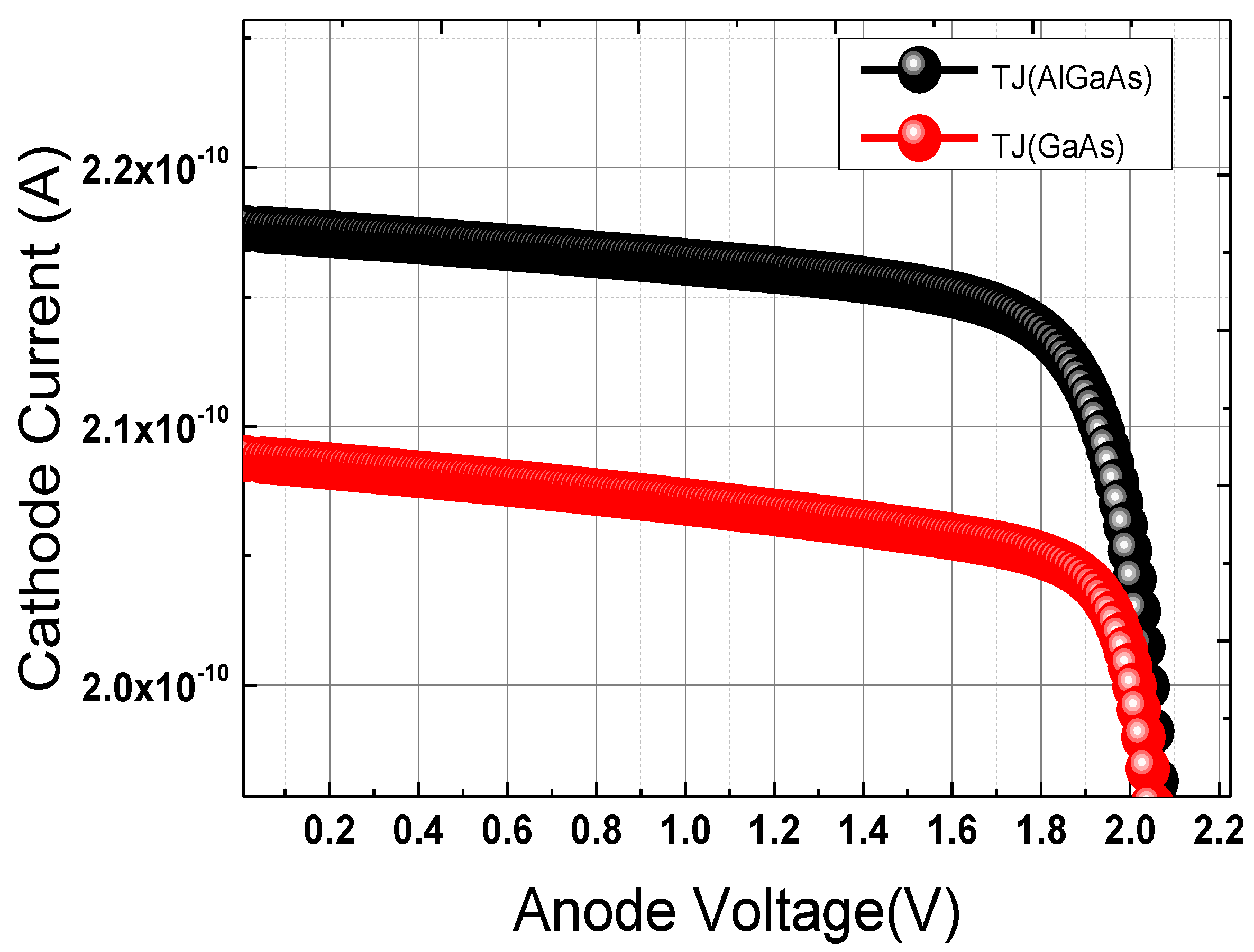
3.3.3. Impact of Tunnel Junction Material on the Performance of DJSCs
The simulation of the structure of multiple junction (MJ) solar cells required the use of two distinct tunnel junction materials; a comparison between the two types of tunnel junction materials is represented in
Table 7.
Figure 10 and
Table 7 highlight clearly the superior performance exhibited by the
tunnel junction compared to the
tunnel junction.
tunnel junctions exhibit superior performance compared to GaAs/GaAs junctions due to their higher bandgap, which minimizes parasitic absorption of photons and allows more light to reach the lower sub-cell. This is achieved through enhanced tunneling efficiency, which is achieved by narrower depletion widths and reduced effective carrier mass, hence facilitating higher tunneling current densities. Additionally, supports heavier doping concentrations with fewer defects, lowering series resistance and recombination losses. This compound material offers enhanced thermal and structural stability, improving its compatibility with sub-cells through better lattice matching. This ensures greater long-term reliability of the solar cell. As a result, tunnel junctions achieve maximum tunneling currents, significantly outperforming junctions, thereby enhancing overall tandem cell efficiency.
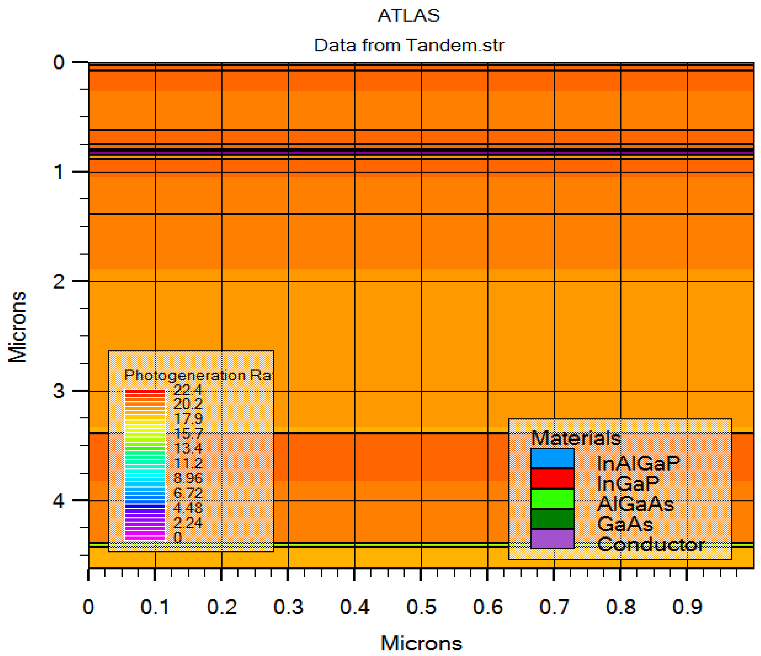
However, it is important to attract attention to the fact that the photo-generation rate (
G) constitutes a central parameter for evaluating the efficiency and performance characteristics of solar cells. This rate is expressed as follows:
where
is the internal quantum efficiency,
is the intensity of the illuminating ray,
is the distance traveled by the ray,
is the speed of light,
is Planck’s constant,
is the absorption coefficient, and
is the wavelength.
Figure 11 illustrates the photo-generation rate of the proposed solar cell model, ranging from 0 to 22.4 cm⁻
3s⁻
1. The highest values are observed in the upper layers, particularly in the
and
regions, where most photon energy is absorbed before reaching deeper layers. Indeed, the
exhibits the highest photo-generation rate due to its superior absorption coefficient (α) compared to
and
, leading to more efficient electron–hole pair generation and improved overall performance.
In contrast, the region shows a lower photo-generation rate, as most light has already been absorbed by the upper layers. This highlights the importance of optimizing the thickness and material composition of these layers to maximize light absorption and hence the efficiency. These results align with previous studies emphasizing the role of material selection in enhancing solar cell performance.
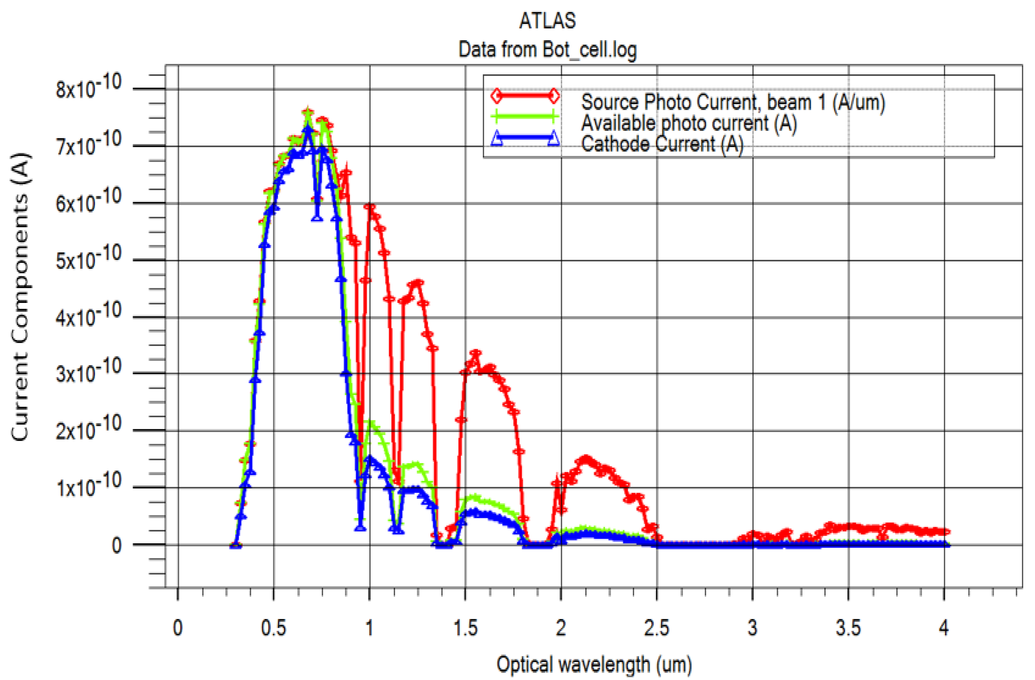
The spectral response is a key parameter in evaluating solar cell efficiency, representing the cell’s ability to convert incident light of varying wavelengths into photocurrent and reducing the photon losses that occur at each stage due to diffusion or absorption. Whereas the spectral response can contain three current components, such as the source photocurrent, the available photocurrent, and the cathode current. Typically, the source photocurrent is the highest, followed by the available photocurrent, while the cathode current is the lowest. Measuring these currents helps assess the incident photon rate (via the source photocurrent) and the photo-absorption rate (via the available photocurrent). Whereas the cathode current represents the solar cell’s output when an anodic voltage is applied. These three components related to the top
solar cell are shown in
Figure 12.
The upper cell, which incorporates the
material with a bandgap measuring 1.9 eV, plays the main role of photon absorber in the ultraviolet and visible part of the spectrum. It is remarkable that, in the visible spectrum, this upper layer shows a notable increase in cathode current generation, as illustrated in
Figure 12.
In contrast, the lower
cell, with a bandgap of 1.42 eV, is designed to capture photons with energies corresponding primarily to the near-infrared light spectrum. The cathode current resulting from this particular configuration is again shown in
Figure 13. In this context,
and
cells prove to be very efficient in absorbing photons with energies close to their bandgap. They are carefully selected based on regions where solar spectra (AM1.5G) display high photon intensity, allowing optimal use of sunlight for electrical energy generation.
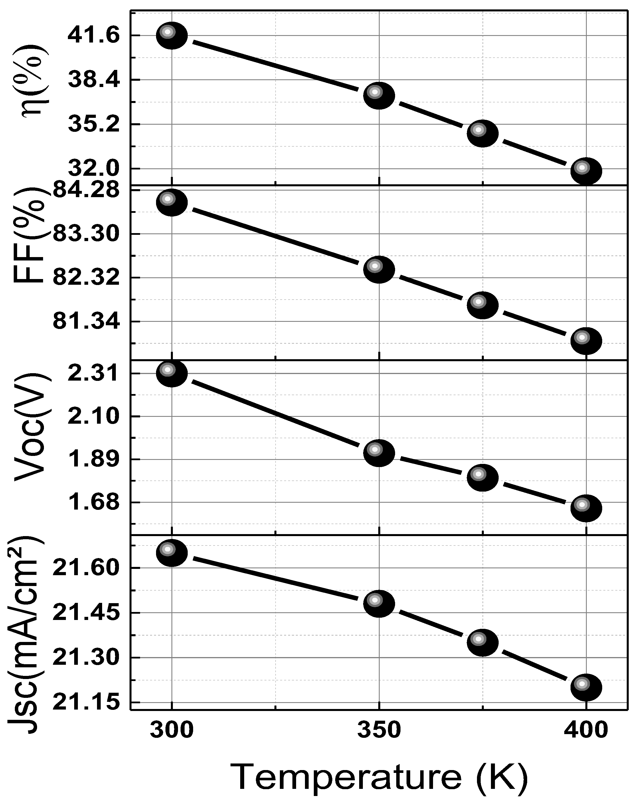
3.3.4. Impact of Temperature on the Performance of Solar Cells
Temperature plays a crucial role in determining the operational characteristics and efficiency of solar cells. Numerous researchers have highlighted the profound impact of temperature on the bandgap of the solar cells [
39]. Indeed, it was proven that as the temperature increases, the energy bandgap of semiconductors tends to decrease, leading to the decrease in the solar cell efficiency. The influence of the temperature on the bandgap is described using the following equation:
where
is the energy bandgap of the semiconductor at temperature
, the
value at
, and
and
are the fitting parameters.
Figure 14 illustrates the impact of temperature on the key performance metrics of photovoltaic (PV) solar cells. As the operating temperature rises from 300 K to 400 K, a noticeable decline in performance is observed across all parameters. The efficiency (
) gradually decreases, starting at a peak value of 41.585% at 300 K and dropping steadily to approximately 31.813% at 400 K, highlighting the adverse effect of high temperatures on solar cell performance.
Similarly, the fill factor (FF) exhibits a downward trend, decreasing from 84.001% at 300 K to 80.92% at 400 K. This reduction in FF contributes significantly to the overall efficiency loss. However, the open-circuit voltage (VOC) declines with increasing temperature, decreasing from 2.319 V at 300 K to 1.65 V at 400 K. This behavior is well-known in solar cells; it is primarily due to the following two key factors: an increase in carrier recombination rates, which reduces charge carrier lifetime, and a narrowing of the energy bandgap at elevated temperatures, leading to reduced voltage output.
In contrast, the short-circuit current density (
) experiences only a slight decline, from 21.65 mA/cm
2 at 300 K to 21.20 mA/cm
2 at 400 K, indicating that temperature has a more pronounced effect on voltage and efficiency than on current density. These trends align with previously published research [
11,
40,
41,
42] reinforcing the understanding that elevated temperatures negatively impact solar cell performance, primarily through reductions in
and efficiency
.
Finally,
Figure 15 shows the characteristic I–V of the optimized
DJSCs investigated in this paper, which demonstrates higher key parameters. Whereas
Table 8 represents a comparison between the key parameters obtained from the studied solar cell and the previous studies on DJ
DJSCs, where it can be seen clearly that the results of the investigated solar cell model in this paper has better key parameter values such as
,
,
, and
, confirming the validity of the proposed structure configuration of the investigated solar cell in producing high electrical energy. This energy will be processed later by power electronics circuits [
43,
44,
45].
3.3.5. Stability Challenges and Enhancement Strategies for DJSCs
Ensuring the long-term stability of (DJSCs) is essential for their durability and commercial viability. This can be met through the design optimization of different used materials and their structure, minimizing the impact of the degradation factors such as thermal stress, moisture, light exposure, and mechanical stress. Indeed, it was proved that the use of optimized wide-bandgap materials like and enhance performance and stability of solar cells by reducing recombination losses. Additionally, optimizing the layers’ properties and applying protective coatings can help significantly in preventing the degradation. However, it was proved that regular monitoring and testing can ensure early detection of different anomalies, allowing for timely corrective measures to maintain optimal performance and reliability.


 ,
, 


