1. Introduction
Silicon oxide (SiO
y) and silicon nitride (SiN
x) thin films are implemented in a vast number of application fields. The tailored mechanical and optical characteristics of SiN
x make it a material attractive for antireflection-, isolation- and passivation coatings in solar cells and CMOS [
1,
2], and for waveguides in photonic integrated circuits [
3,
4]. High quality dielectric isolating materials are further implemented as so-called high-k dielectrics in MOS devices [
5]. Key applications in the optical domain are Bragg mirrors composed of a low refractive index material, frequently SiO
y, and a high refractive index material [
6]. An alternating multilayer sequence of quarter wavelength layers results in a reflectivity very close to 100% due to constructive interference in reflection, given by the negligible loss of the materials. These mirrors outperform metal mirrors that scarcely exceed 98% reflection, resulting in considerable losses for systems with many mirrors. The larger the refractive index contrast between both dielectrics, the larger the block bandwidth. As there are hardly any solid, mechanically stable, and low loss materials with a refractive index below that of SiO
y (
n~1.45), increasing the refractive index contrast of the high index layer is the only viable option for increasing the block band width. Silicon carbide (SiC
z) is a sensible option in the visible domain with a refractive index around 2.6 that decreases with increasing wavelength. In the telecom band, however, non-crystalline SiC
z as deposited with typical PECVD processes, features non-negligible losses [
7], deteriorating the mirror quality.
A further physical parameter that can be utilised in PECVD films to achieve functionality is the tunable stress that allows for implementation in microelectromechanical systems (MEMS) [
8,
9]. An example of a tunable optical filter is illustrated in
Figure 1a. It consists of a MEMS-tuned microcavity where both stress and high refractive index contrast to SiO
y are essential in order to obtain a functional device [
10,
11]. The filter is composed of a Distributed Bragg Reflector (DBR)-based MEMS Fabry–Pérot (FP) cavity, where a temperature- or electro-statically tuned concave Bragg reflector MEMS is grown on top of a static, flat Bragg mirror. The air gap (
Lcav) between the top and bottom mirrors that is achieved by depositing the top Bragg mirror with compressive stress and subsequently releasing it, determines the free spectral range (FSR) of the cavity [
12]. For carefully chosen reflectivities of the two Bragg mirrors, the filter structure features a spectrally very sharp, tunable transparent notch within the block band when the effective cavity length
Leff equals multiples of a half wavelength as illustrated in
Figure 1b. By applying heat or an electrostatic force, the MEMS mirror can be deformed, leading to a change in
Lcav and consequently a widely tunable transmission filter. Also here, a large refractive index contrast between the individual Bragg layers has several advantages: (i) much fewer periods are required to achieve a target block band reflectivity, (ii) a larger block band and free spectral range, (iii) less inertia and thus faster tuning speed in case of electrostatic tuning, and (iv) less thermal mass and thus faster tuning speed in case of thermal tuning.
High quality films are frequently deposited with plasma-enhanced chemical vapour deposition (PECVD) that allows to tune the chemical composition as well as the stress of thin films. Low temperature PECVD is essential for deposition of dielectric materials with high thickness precision over temperature-sensitive materials. PECVD deposited SiN
x had been studied in terms of refractive index showing results in the telecommunication range from 2 to 2.6 at a chamber temperature of 80 °C and even up to 3.08 for higher temperatures [
2,
3,
4]. Thin films of this material have also been characterised in terms of stress gradient, from compressive to tensile values and their Young modulus (
E) through various techniques [
13,
14,
15]. Both parameters are essential for designing the MEMS-tuned cavities where the material stress in the MEMS Bragg reflector determines its radius of curvature and the optical parameters its reflectivity and absorptive loss. For cavities with high quality factors as well as for implementation as tuning elements in VCSELs [
16] that feature much less gain per round trip as in-plane DFB or DBR lasers, the loss tangent of the material must be as low as possible.
Besides application in lasers, tunable MEMS find their applications in spectroscopy, optical communication or optical imaging [
17,
18,
19], amongst others. The MEMS design developed in this study and the desired characteristics are meant as tunable transmission notch filter within a large gain bandwidth laser’s cavity for their application in swept source optical coherence tomography (SS-OCT). For this reason, our goal is to design a device with low MEMS mass for fast tuning, wide block band and small cavity length for large free spectral range and low absorption in the 1550 nm range as these parameters will determine the characteristics of the tomographic image [
20].
In this study, we first investigate the refractive index, extinction coefficient, the stress gradient, and roughness of single silicon-rich SiNx film applying different recipes. Then, selecting the most suitable recipe for our application we deposit and characterise a silicon-rich SiNx/SiOy DBR. As final step, we develop a movable membrane with different architectures, selecting one of the designs, we studied its electro-thermal tuning behaviour and through simulations we estimate the Young’s Modulus of silicon-rich SiNx of that specific recipe.
2. Materials and Methods
A Plasmalab 100 ICP 180 from Oxford Instruments Plasma Technologies (Bristol, UK) at a substrate temperature of 80 °C and an inductively coupled plasma (ICP) generator at a radio frequency (RF) of 13.56 MHz with an optional additional RF field between the electrodes is the modular plasma processing system employed in this study. Two-inch boron-doped (100) silicon wafers with a thickness of 280 μm are used as substrate. We implemented different parameters of gas flow ratio, RF power, and chamber pressure, for growth of thin films of silicon-rich SiN
x at a deposition duration of 15 min. The precursor gases used in this deposition are N
2 and SiH
4, avoiding the absorption centres that NH
3 creates [
3].
For every recipe, refractive index (
n), extinction coefficient (
k), and deposition rate (DR) are determined using ellipsometry (Sentech 850) at an incidence angle of 70°. In this methodology, a Cauchy model is employed in order to determine these parameters [
21]. Then, the roughness of the film is measured using a Dektak 6M Stylus Profiler, as well as the curvature of the substrate before and after deposition, that allows the evaluation of the stress gradient of the layer using the bending plate method [
22].
Once the parameters of refractive index, roughness, and stress are determined, applying different processes of etching and evaporation techniques, following a similar protocol to the one described in [
12], we fabricated on wafer hundreds of MEMS-FP cavities with 9 different architectures. Each of these filters consists of a plane concave cavity formed by a bottom and a top DBR with two different electrodes on top of each mirror. A 6-layer pair of quarter-wavelength silicon-rich SiN
x and SiO
y DBR deposited over a double side polished substrate of boron-doped (100) silicon wafer with a thickness of 280 µm forms the plane part of the cavity. Over this bottom reflector is deposited a second DBR, in this case with 6.5-layer pairs and a concave shape. The curved structure forms as a result of the compressive stress of the layers and a chromium sacrificial layer (of height
h0, c.f.
Figure 1a) that separates both reflectors during the fabrication process resulting in the final air gap (
Lcav). The SiO
y layers of both DBR were deposited with a flow of precursor gases 12:3 sccm SiH
4:N
2O, an IPC power of 500 W, an RF power of 75 W at 7.5 mTorr of chamber pressure. SiO
y features a DR of 15.5 nm/min, a refractive index at 1550 nm of
n = 1.4476 and a compressive stress of 130 MPa. The reflection band of the DBR is measured using ellipsometry at 40°, the minimum angle achievable by the ellipsometer in order to have a measurement as close to 0° as possible.
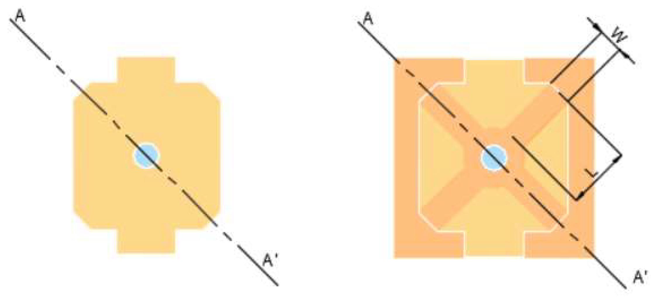
Figure 1a shows a schematic cross-sectional image of a MEMS-FP cavity. The geometry of the FP-cavity bottom and top electrode are illustrated in
Figure 2 where the width (
W) and length (
L) of the arms are altered for every architecture while the central ring in the top electrode that connects the four arms keeps a constant external radius of 40 and an internal radius of 25 ± 1 μm. This hole is the optical window.
Using the Dektak stylus profilometer, we measured the curvature of every architecture. Then, the nine architectures are simulated in Comsol Multiphysics in order to derive from the measured curvature the required the values in Young’s modulus,
E, of the silicon-rich SiN
x deposited in the DBR assuming a Poisson’s ratio of 0.27 [
11].
A CTL 1550 tunable diode laser from Toptica Photonics (Gräfelfing, Germany) with a tuning range from 1510 to 1630 nm was used as laser source for the tuning characterisation of one of the designs. The laser is focused on the active device that features an optical window diameter of 13.5 µm by a collimator with a focal length of 12 mm combined with a micro focus lens of 8 mm focal length. A photodetector captures the transmitted power of the laser through the FP-filter that tunes its whole range at 0.1 nm/s at a stabilized temperature thanks to a Peltier element while different values of current are applied on the top electrode in order to tune the FP-cavity electrothermally.
3. Results
Table 1 shows the precursor gases flow (sccm), the IPC power (W), the RF power (W), and the APC pressure (mTorr) used in every recipe along with the average results of various deposited films in DR (nm/min), stress gradient (MPa), roughness, refractive index
n and extinction coefficient
k at 1550 nm for seven investigated recipes.
The design goal of the recipe is to achieve an as high as possible refractive index, a
k-value below 0.0124 and a compressive stress inferior to 150 MPa in absolute value, in order to overcompensate the stress of the SiO
y quarter wavelength layers of about 130 MPa compressive. These characteristics are necessary to achieve functional MEMS mirrors in mechanical and optical terms. The limit for the extinction factor
k is chosen such that the absorption constant at 1550 nm,
is below 1000/cm. The roughness should be as low as possible while the deposition rate is secondary. First, we determined approximate process parameters in preliminary work (not shown here).
Table 1 shows the final optimisation step.
In
Table 1, the recipes can be classified in two groups, in the first one (recipes 1 to 3) the flow volume of SiH
4 is of 9.8 sccm, and the second one (recipes 4 to 7) with 9.6 sccm of SiH
4. In both groups, the roughness increases dramatically when RF power is introduced while the refractive index, stress gradient, and the deposition rate increase and the extinction coefficient decreases (recipe 2 and 6). In deposition 3, the APC pressure was reduced by 0.3 mTorr giving as a result a decrease in the refractive index and an increase in stress with respect to deposition 1 and 2. A similar situation occurs in deposition 4 where the APC pressure is decreased by 2 mTorr, compared to recipe 5, in this case both refractive index and stress show a rise. On the other hand, when this pressure is increased (recipe 7) both refractive index and stress are reduced.
From all the seven recipes, depositions 2 and 4 show the optical and mechanical characteristics that are best suited for the MEMS. Their characteristics are very similar, both have a high refractive index, a low absorption, and their stress gradient is inside the desired boundaries. Recipe 2 was dismissed due to its high roughness, with recipe 4 as the material selected for the fabrication of the FP-filter reflectors.
Figure 3 shows the measured reflectivity of a 6.5-layer pair silicon-rich SiN
x/SiO
y DBR deposited with the silicon-rich SiN
x deposition parameters 4 in
Table 1 and the growth conditions described for SiO
y in the methods section. This reflection corresponds to the top-DBR of the FP-filters described in this manuscript. The expected total thickness is 2716 nm. The σ-polarisation provides a refection band (
R > 96%) in the range from 1140 to 1620 nm and in the case of π-polarisation this range goes from 1220 to 1480 nm. This figure also presents the theoretical reflectivity at 40° and 0° of incidence angle, yet with a slightly higher reflectivity of
R > 98%. Spectrally, the theoretical graph matches with negligible differences the measured curve. The simulation of reflectivity at vertical incidence angle offers a reflectivity band from 1280 to 1640 nm with
R > 97%. The central wavelength shifts to longer wavelengths compared with the 40° curves. We remark that at 1700 nm, the structure still shows a reflection of
R = 94%.
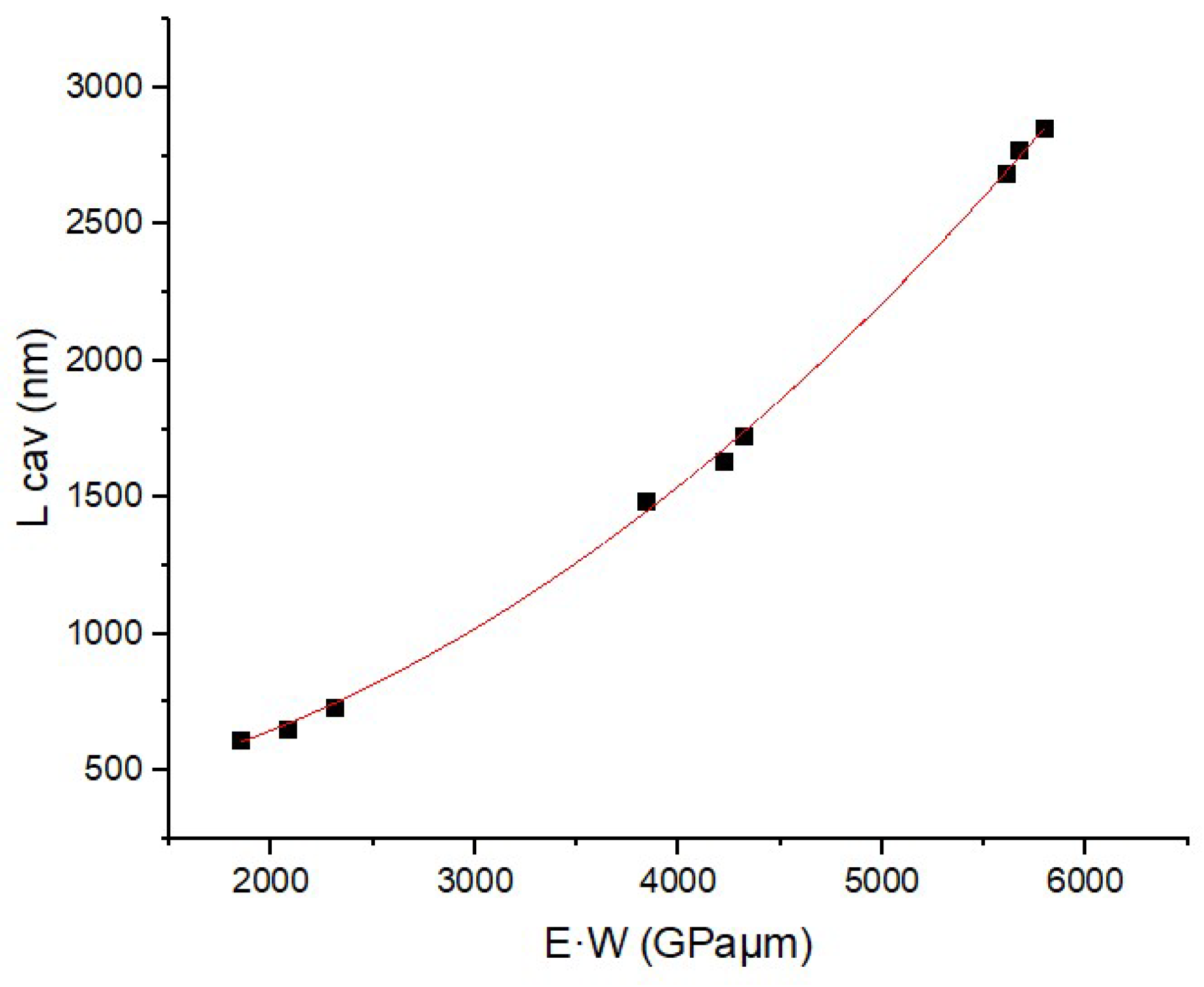
Table 2 summarises the 9 different architectures for our MEMS ordered from smaller to larger electrode area (
A), the cavity length (
Lcav) in nm and Young’s modulus
E in GPa.
The cavity length, i.e., the distance between the MEMS mirror and the bottom Bragg mirror depends on the MEMS architecture with two main empiric findings: (i) for low areas of the arms
, the elastic modulus scales approximately linearly with arm area as more material is compressively stressed. The elastic modulus saturates around 90 GPa for an area around 1000 µm
2. There is only one exception, namely,
; however, the elastic modulus of the next smaller case is within the error bar of the simulation. (ii) The cavity length scales about quadratically with the product of elastic modulus and width,
as
Figure 4 shows. This feature can be used as design rule for cavities.
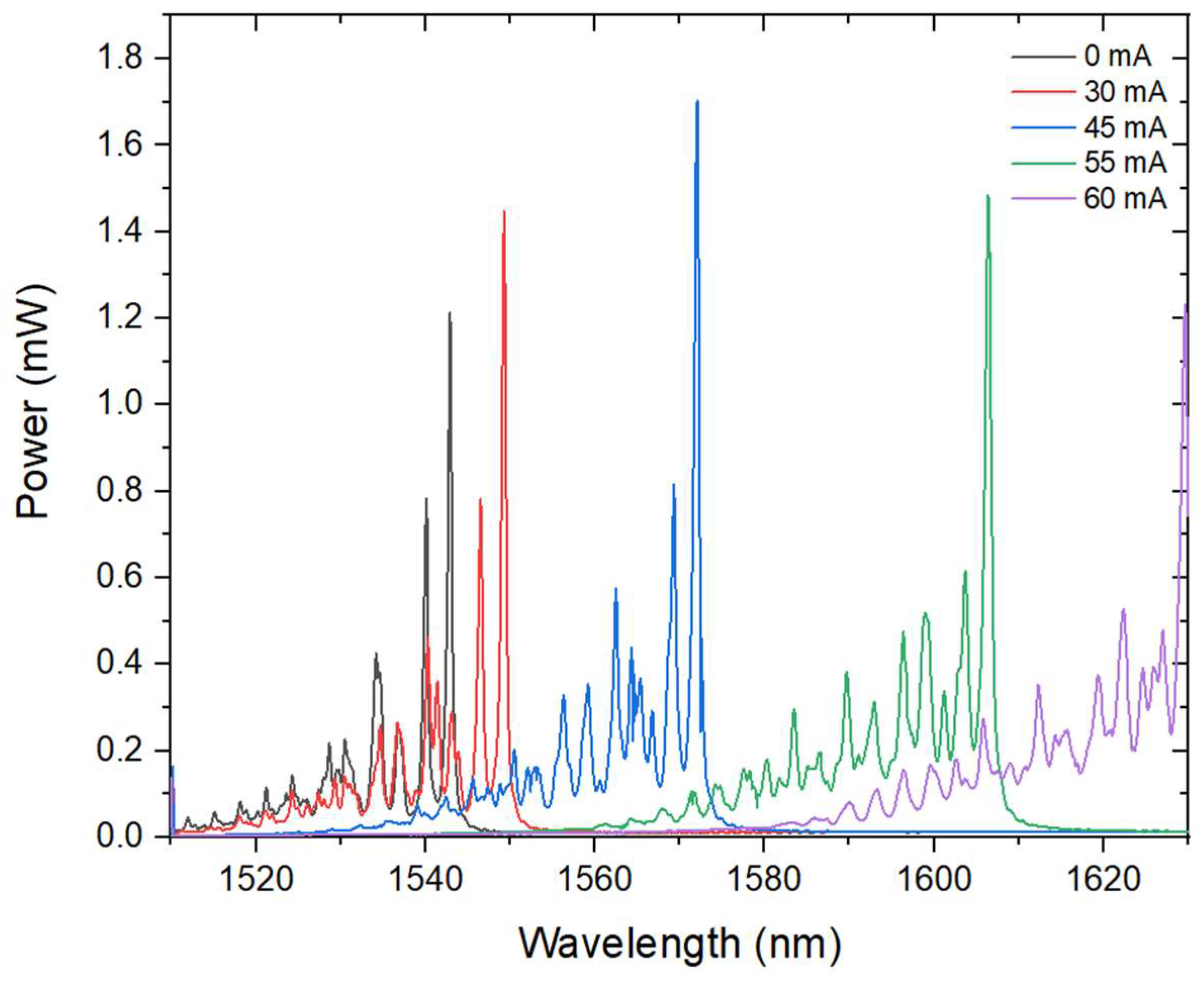
Figure 5 shows the tunability in transmission for a FP-cavity with 23 µm long and 33 µm wide arms, corresponding to a cavity length of 651 nm (c.f.
Table 2). At zero bias, the main transmission resonance is centred at 1542.9 nm, i.e., in the middle of the C band. Upon thermal tuning, the main transmission peak shifts out of the range covered by the tunable diode laser, yet reaching a peak wavelength of 1629.6 nm at a tuning current applied to the top electrode of 60 mA while keeping a constant base temperature of 16 °C. The full width half maximum is 0.70 ± 0.1 nm, averaging overall the main peaks shown in the figure.
4. Discussion
From the seven recipes of
Table 1, we find the highest refractive indices in recipes 2 and 6. In both recipes, RF power is introduced into the process. This produces an increase in the refractive index, the deposition rate, the compressive stress, and the roughness of the thin film. This last parameter, the roughness, makes these thin films inappropriate to be used for the DBR deposition due to the high number of defects that it creates, even if the stress characteristics and the extinction coefficient fit our objectives. These changes occur because the RF power potentiates the attraction of the plasma generated in the ICP coils to the substrate during deposition creating a denser plasma at the sample surface [
3,
9,
23]. Further options not considered here would have been to increase the SiH
4:N
2 ratio providing higher refractive index, but also the absorption in the 1550 region rises and depending on the pressure, this can lead to stress gradients out of the MEMS requirements. This can, to a certain degree, be compensated with the chamber pressure to obtain a balance between refractive index and stress gradient as demonstrated in refs [
1,
3,
24]. Further alternative recipes demonstrated in the literature use NH
3 as precursor gas, and dilution with Argon for generating a more uniform heat distribution in the chamber. The use of NH
3, however, results in N-H dangling bonds with absorption in the C-band and thus disqualifies for low loss DBR membranes at telecom wavelengths. But it is a viable option for low loss material in the 300 nm to 1100 nm range [
25] where our recipe is lossy. Argon could help for a more uniform distribution; however, it caused plasma instabilities in our system. This led us to choose recipe 4 to be employed for the DBRs that form the FP filter. It provides a much higher refractive index as compared to stochiometric Si
3N
4 (
n~1.95) and sufficiently low extinction coefficient while keeping its stress inside the required parameters that allow functional MEMS. Other studies have achieved higher refractive index with the same deposition temperature and precursor gases as in [
2] where the refractive index has a maximum value of 2.6. Nevertheless, this study used low pressures that are not achievable with the PECVD machine employed in our study, and RF power that as already mentioned causes excessive film roughness, incompatible with DBR deposition.
Figure 3 shows the reflectivity band of the FP-filter’s top DBR, that covers two important wavelength ranges, namely, 1310 and 1550 nm. Using the matrix method, the theoretical reflectivity and stopband of this DBR is of 0.997 and 510 nm, respectively, under vertical incidence. The ellipsometric measurements shows inferior results, this is because of the angle at which ellipsometry was performed makes the reflectivity band less broad than it would be at 0° measurement and the incidence angle causes a shift in the centre wavelength towards shorter wavelengths as described in [
26]. This effect can be noticed when comparing the 40° reflection bands plotted in the figure with the simulation at vertical incidence. A similar work on DBR was performed by [
9] though with different reflectance band centre. This study used PECVD at 75 °C with no RF power obtaining values of stress that flows from compressive to tensile with a refractive index in the 1550 nm range of about 2 using the same precursor gases that were applied in our depositions. It shows a reflective band of 260 nm that is almost half of the bandwidth achieved in this manuscript in π-polarisation using 11.5 layers of SiN
x/SiO
y. In our study, the number of layers is about halved for the same reflectivity because the refractive index difference between our layers is almost 20% higher than in the mentioned study. This optimisation compared with previous work is beneficial in terms of increment of tuning speed and FSR of the MEMS devices due to the reduction in mass and in cavity length [
12,
27].
Besides obtaining a reduction in the top electrode mass and cavity length due to changes in the MEMS composition, their geometry also plays an important role in the optimisation of these characteristics. As
Table 2 shows, the length of the cavity increases as the width and the length of their arms do. This table also illustrates the results on Young’s modulus product of the finite element simulation of every architecture. These results are lower compared with [
11] where SiH
4/NH
3/N
2 were used as precursor gases and a Young’s modulus in the range between 240 and 320 GPa was calculated by membrane point deflection with a substrate temperature of 300 °C. Such high values would lead to excessively large
Lcav and thus reduced free spectral range. Results in the same range applying nanoindentation methods and using SiH
4/NH
3/N
2 as precursor gases was obtained in [
15], a study that also demonstrates how the value of
E is affected by the substrate temperature. The nanoindentation method was also applied in [
8] where an
E of 97 GPa at 125 °C of deposition was obtained. To our knowledge, there is no study in
E where SiH
4/N
2 were used as precursor gases at temperatures inferior to the already cited. Taking into account the mentioned studies, the increase in Young’s modulus with the substrate temperature and with the increase in H-N bonds that the use of NH
3 introduces, the results of our study are reasonable [
28].
Figure 5 shows the electro-thermal tunability characterisation of one of the fabricated architectures. By comparing to
Figure 1, we actually expect a single peak. The further resonances besides the main resonance appear most likely because of imperfect coupling to the resonator, exciting undesired (off-axis) modes or with light outside the central hole of the main cavity. Their amplitude can be reduced by improved coupling schemes, exactly matching the window size and required NA of the filter. This goes beyond the investigations in this manuscript. For applications in a laser, only the dominant mode will survive as long as there is sufficient gain.
In the following, we estimate the maximum tuning range limited by the rupture limit of the device at 80 mA current. The main peak reaches the maximum tuning wavelength of the CTL by applying a current of 60 mA through the top electrode. The investigated device shows a tuning range of 86.7 nm as compared to the case without any tuning current. As the heat delivered to the MEMS mirror scales quadratically with current, we expect a quadratic temperature and thus length change in the cavity, resulting in a maximum tuning range of 156 nm, corresponding to a maximum wavelength of 1698 nm where the reflection is still
94%. However, in previous experiments with MEMS-tuned VCSELs [
29], we see a super-quadratic increase, possibly caused by the interplay of heat dissipation and the fact that the MEMS is curved, i.e., a linear increase in circumference results in a non-linear change in cavity length. In the results presented in
Figure 5, we see an empiric tuning with a cubic current dependence, resulting in a maximum tuning range of 208 nm. The resulting maximum wavelength of 1750 nm is, however, outside the block band of the MEMS, which would likely result in a mode hop. But even a tuning range of about 156 nm is to date only achievable with external, grating-tuned cavities that are orders of magnitude physically larger than the demonstrated device. The wavelength at 0 mA tuning current (being in the midst of the stop band of the investigated device) can be tuned by the cavity length during manufacturing and fine-tuned during experiments by the base temperature, allowing full use of the maximum tunability.
The designed MEMS structures are well suited for implementation in VCSELs where tuning ranges between 40 nm and 103 nm have yet been demonstrated [
16,
30,
31]. We remark that the tuning range of MEMS-VCSELS is usually limited by VCSEL gain and not by the filter bandwidth. One of the smallest cavity size demonstrated in this manuscript is of the order of 650 nm, being several times smaller than MEMS-tuned cavities investigated in vertical cavity diode lasers (VCSELs). We, thus, do not expect any mode hops over the complete tuning range. This is supported by the fact that no new modes arise at the lower tuning end of the CTL when the current is increased until the rupture limit of the cavity. The tuning continues towards wavelengths higher than 1630 nm as it was already expected from the simulation of
Figure 1b, the reflectivity profile of
Figure 3, and the theoretical reflectivity mentioned in the
Section 3 calculated by the matrix method. Other authors have achieved 112 nm with DBR-based FP-filters in terms of wavelength tuning by employing similar kind of dielectric materials [
27]. Other more complex and bulk MEMS designs in the near-infrared region can tune from 1479 to 1590 nm as in [
32] in this case avoiding the mechanical disturbances that suspended multilayer MEMS suffer, yet still considerably less than the extrapolated tuning range of 156 nm reported in this manuscript.
5. Conclusions
This work reports the study of low temperature deposited PECVD silicon-rich SiNx thin films. These films were characterised in terms of refractive index, extinction coefficient, and stress gradient for different deposition conditions. The most adequate recipe was then employed to form a silicon-rich SiNx/SiOy DBR with a broad band reflection centred at 1400 nm with a stop band width of about 360 nm for perpendicular incidence. The mechanical characteristics of SiNx were essential in order to fabricate a DBR-FP filter that forms a suspended membrane structure supported by four arms, as these characteristics define the distortion of the membrane and affect the performance of the filter. The MEMS-FP filters were fabricated with different geometries, providing each of them a different cavity length. The cavity lengths obtained from about 650 to 2850 nm translate in a FSR at 1550 nm of 1850-420 nm, respectively, being larger than the block band size, a fact of high importance for tunable, single-moded filters in order to achieve mode-hop free tuning.
Of all the nine fabricated designs, one of them was selected to be characterised electro-thermally. By applying current from 0 to 60 mA, the studied FP-filter achieves a tuning range of almost 90 nm centred at 1585 nm in wavelength. We expect a tuning range of at least 156 nm by applying the maximum permissible current of 80 mA before thermal destruction of the mirror occurs.
As a final step, by putting the cavity length of every fabricated filter into a finite element software, COMSOL Multiphysics v.4.1, we estimated a Young’s modulus of SiNx from 56 to 90 GPa. The results obtained in this study are essential to investigate new geometries that can improve the performance of MEMS-FP filters and will allow more precise simulations.


