
Topological and Fractal Analysis of Nanostructured Metal–Dielectric Films

 , ,
, ,  and
and 
Abstract
1. Introduction
2. Materials and Methods
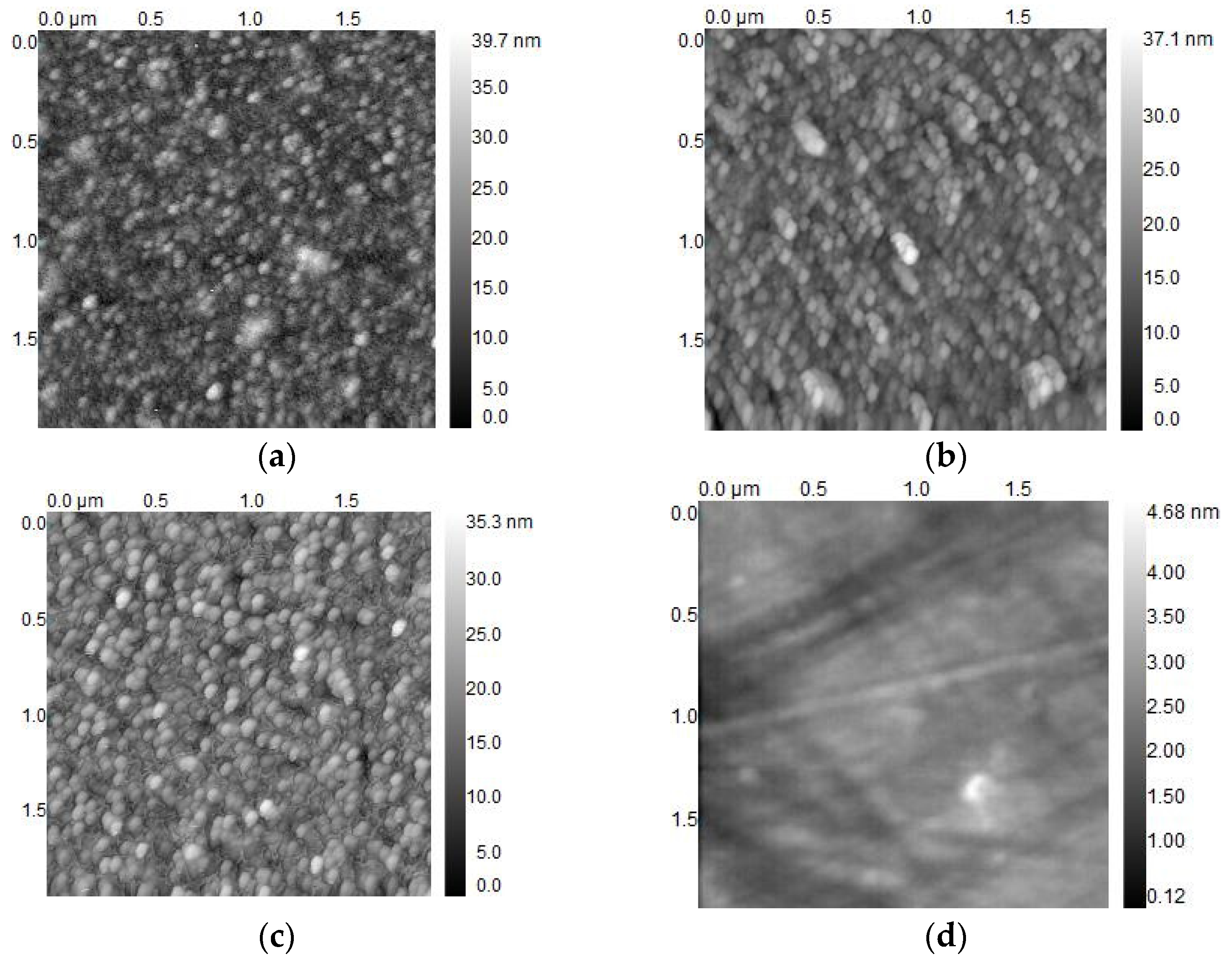
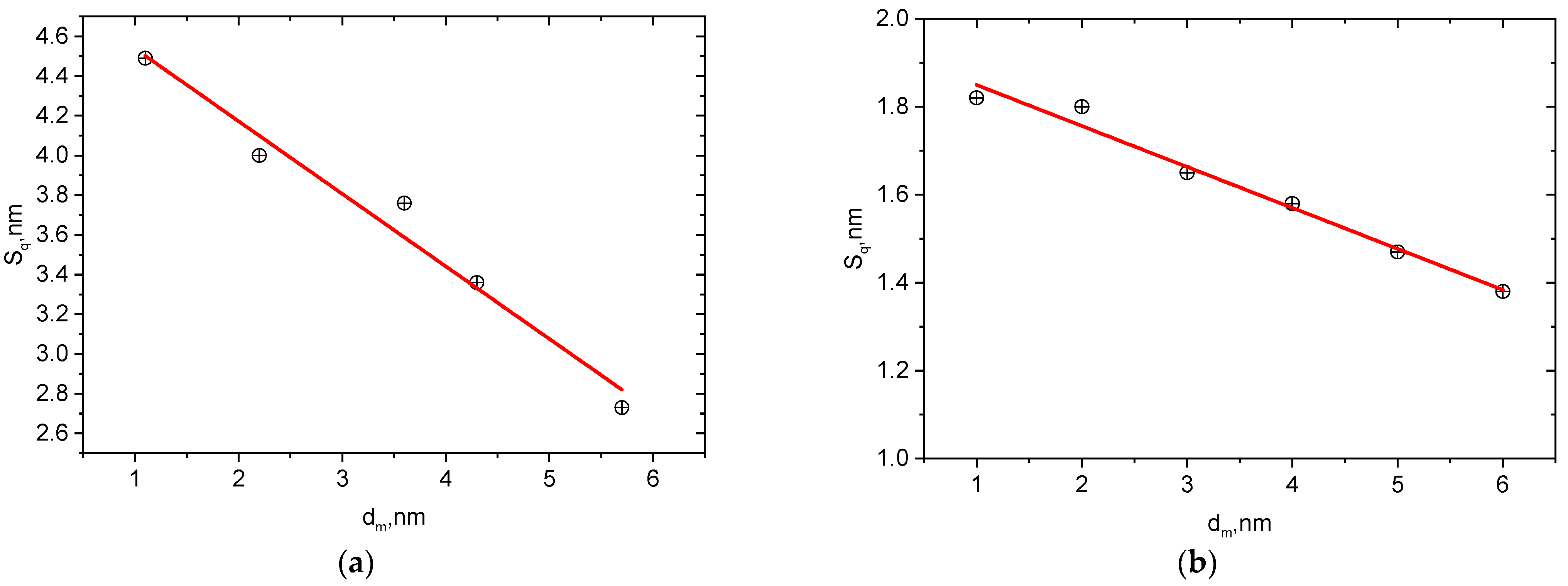
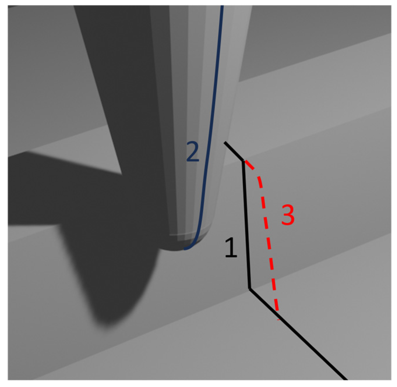
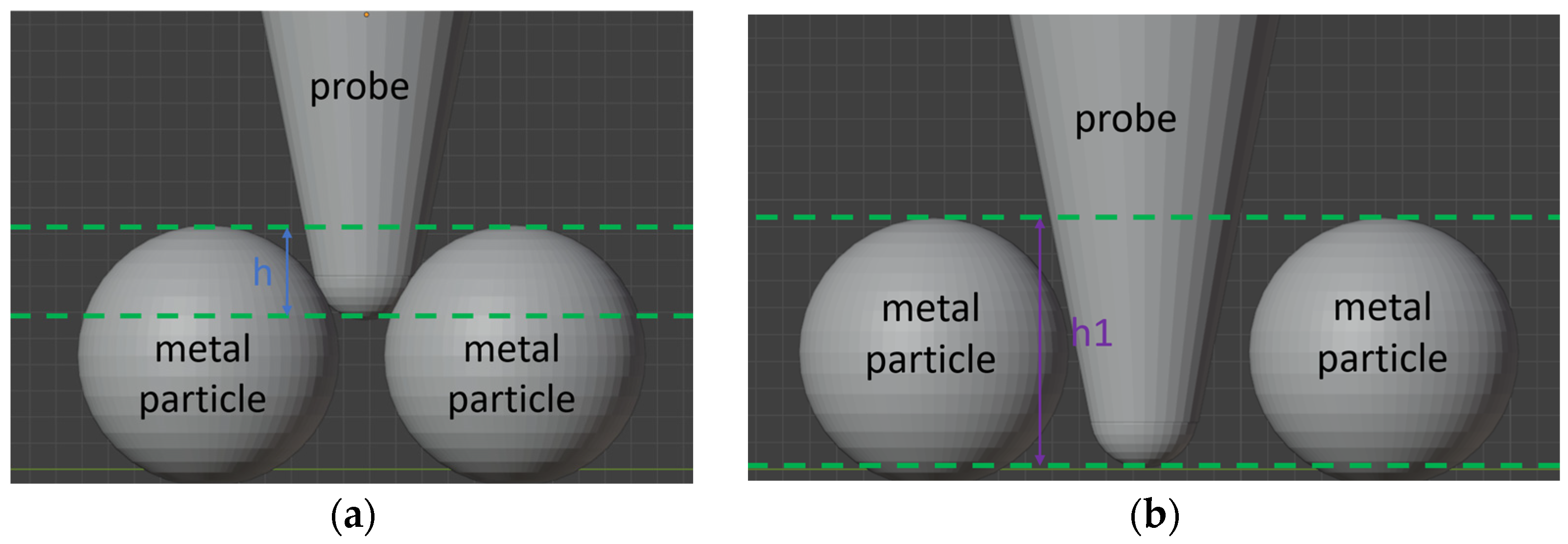
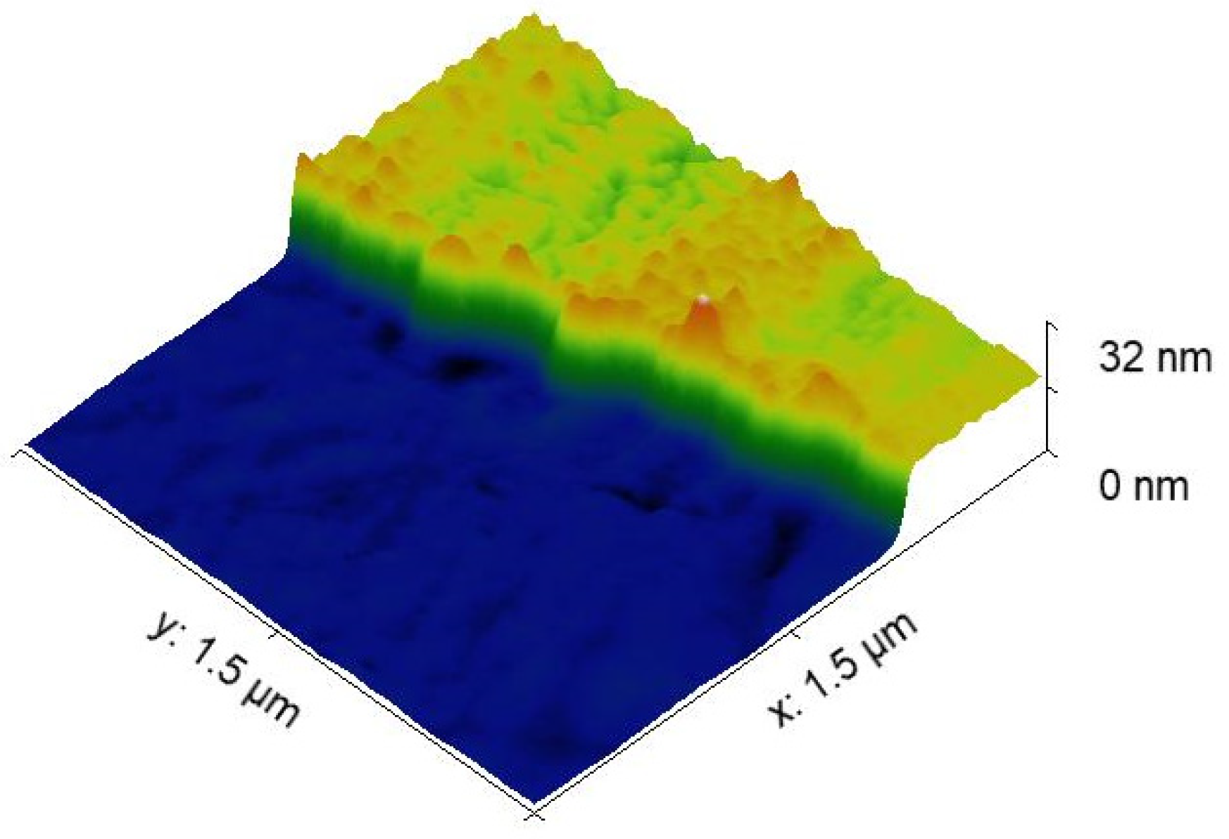
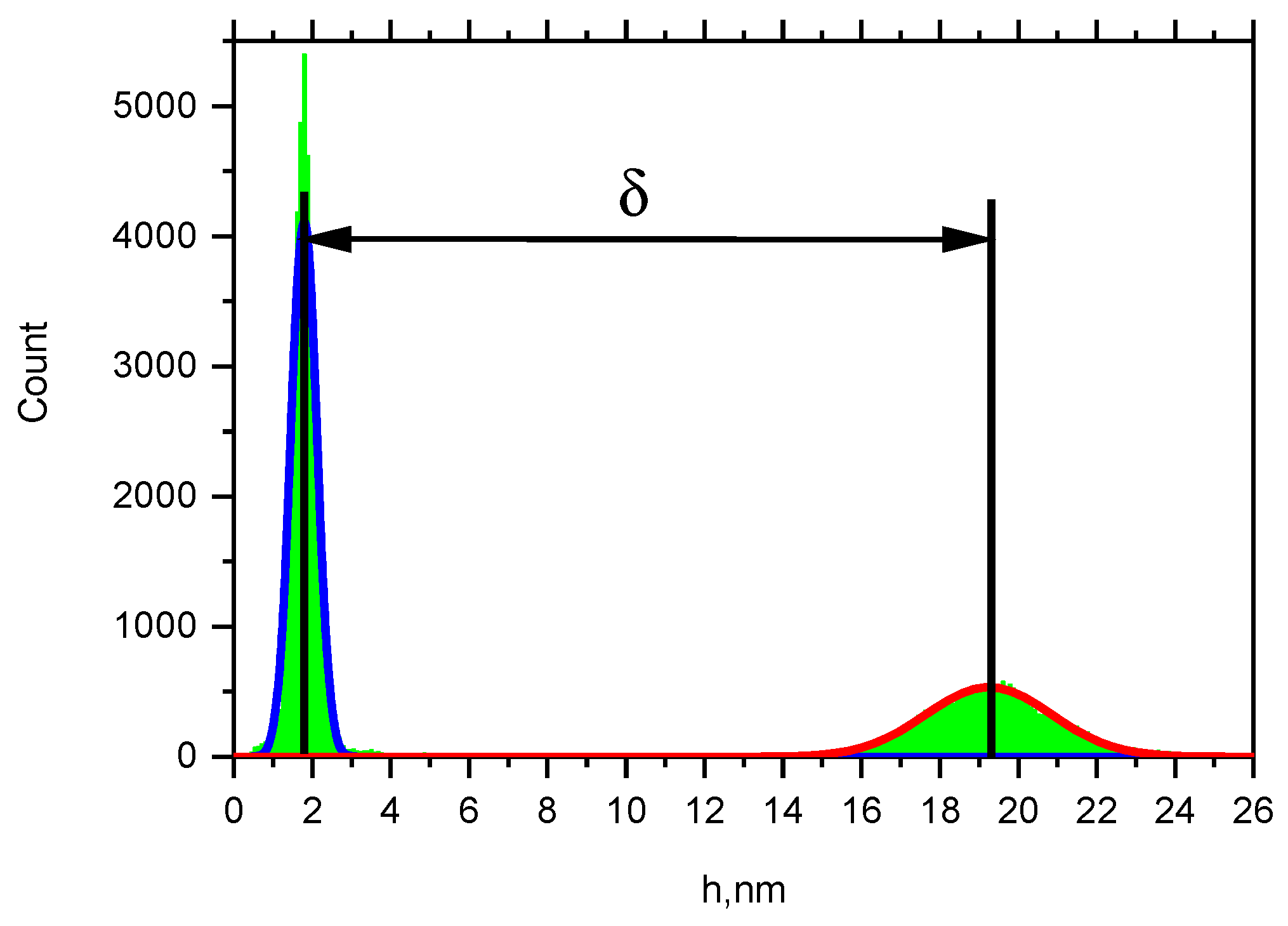
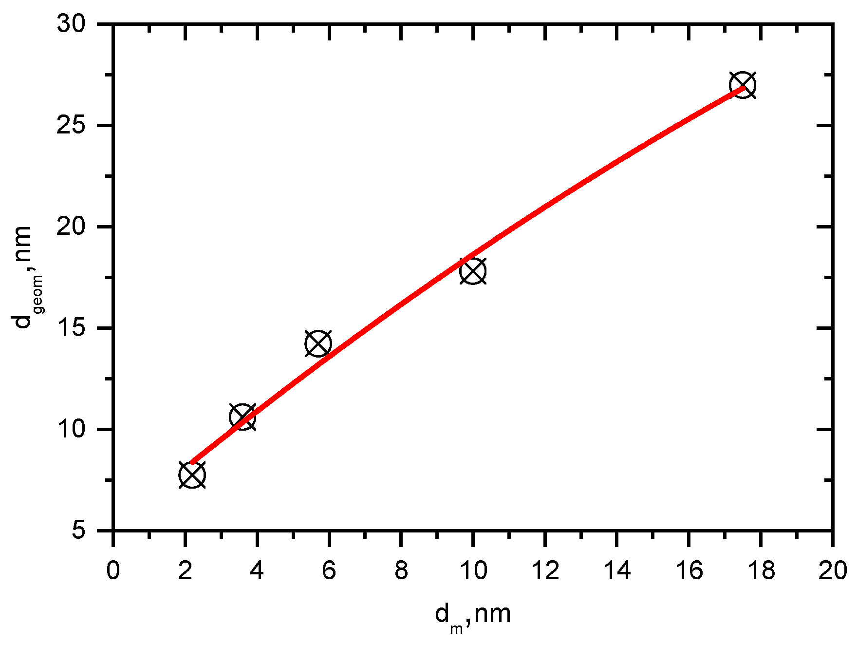
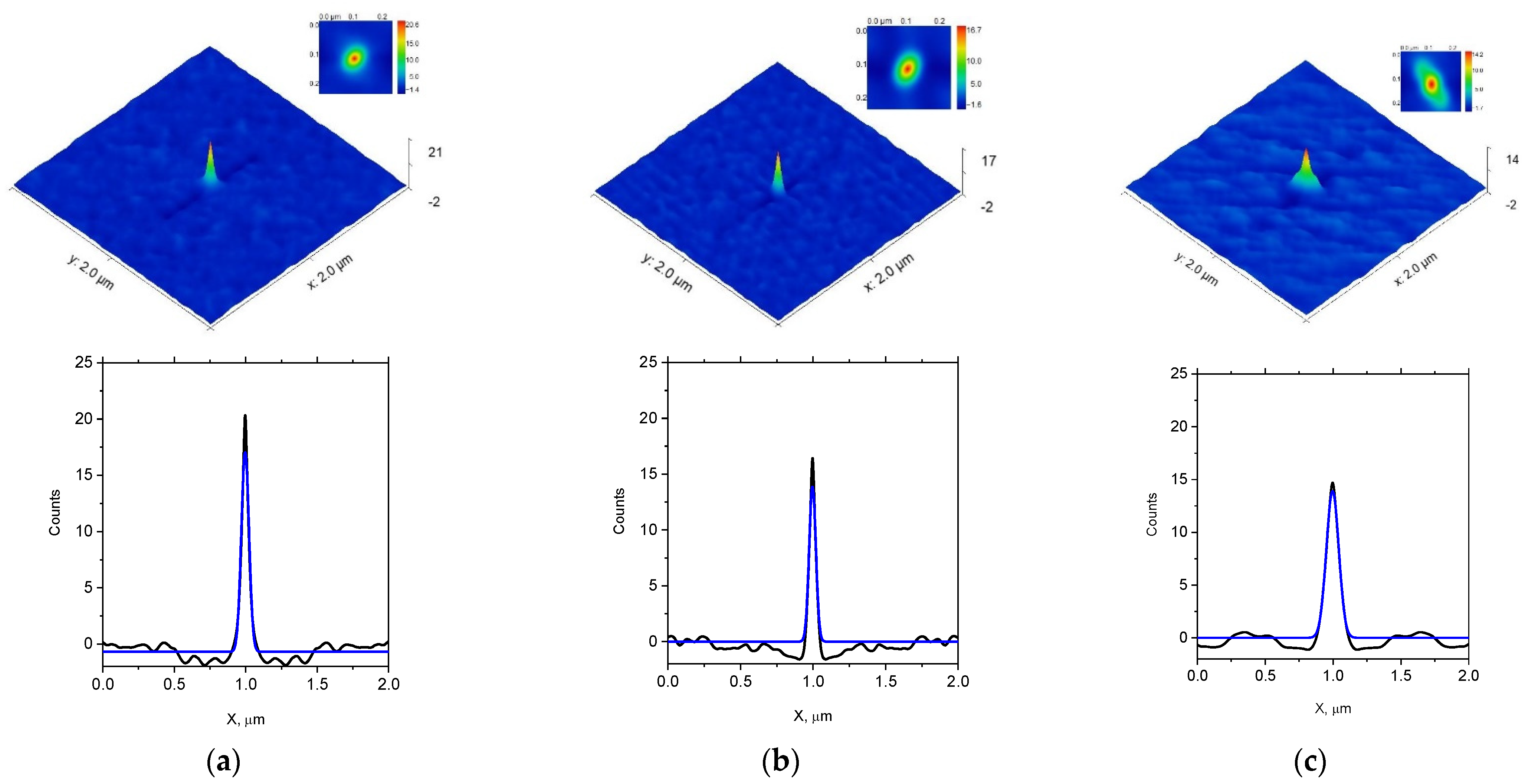
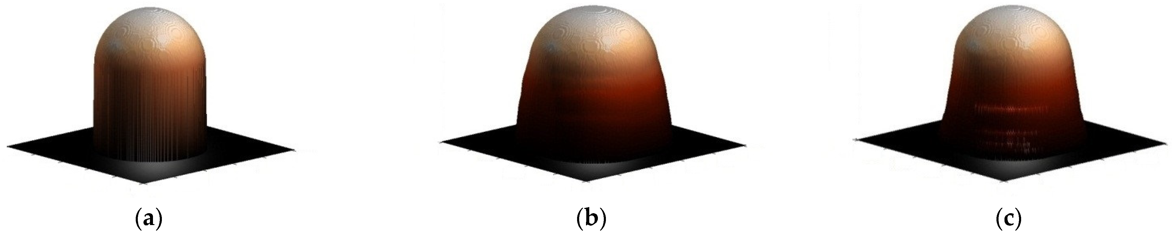
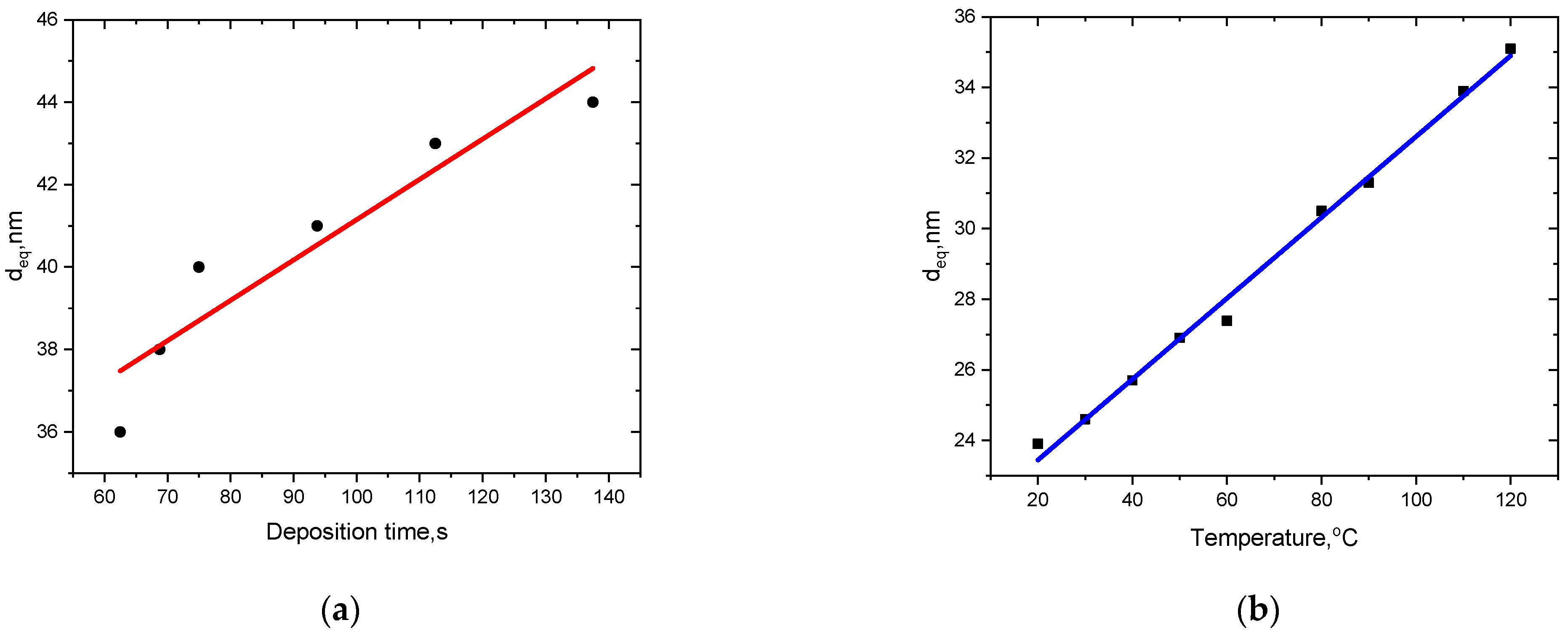
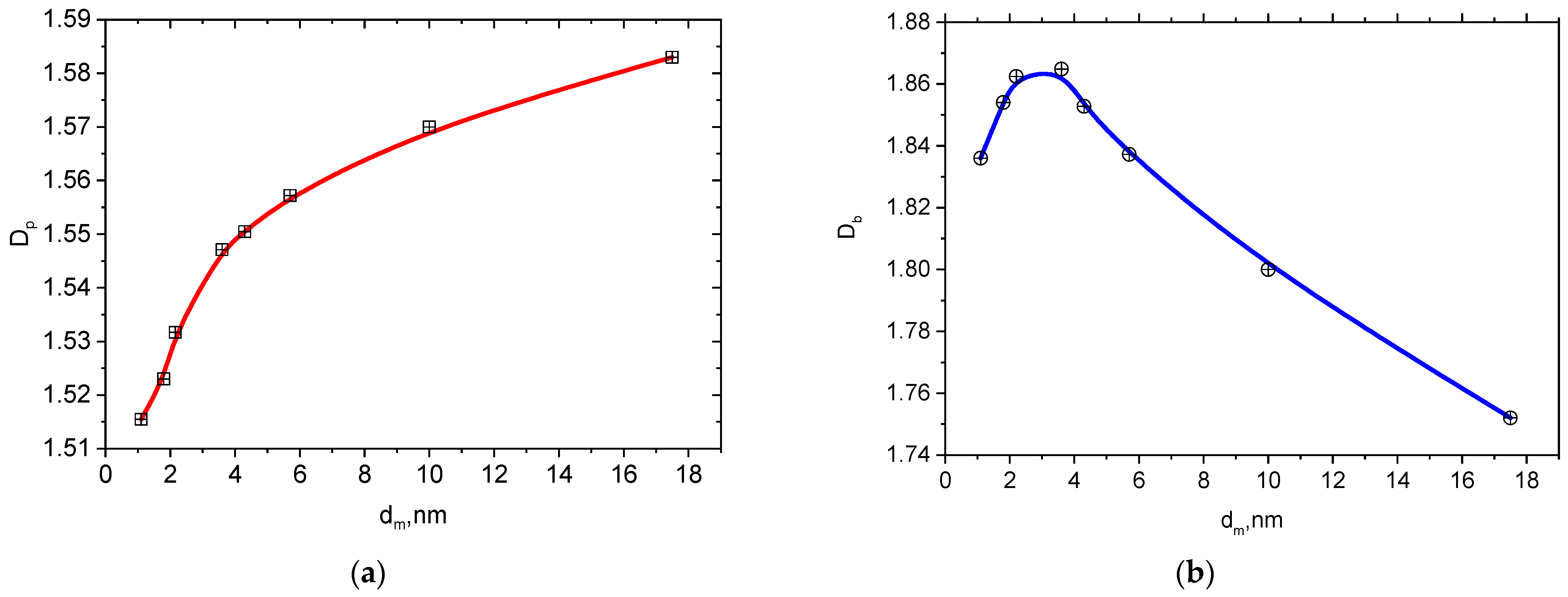
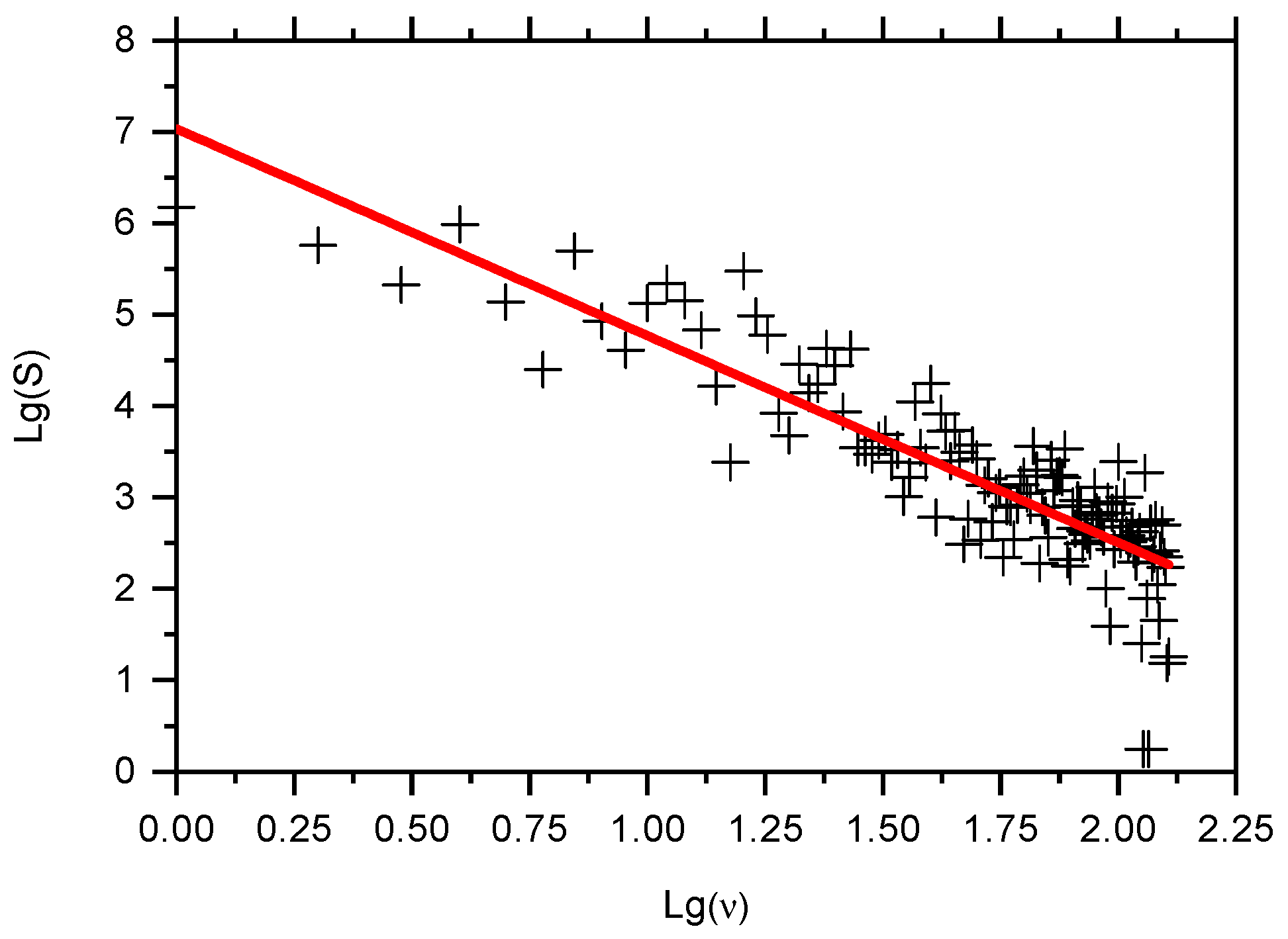
3. Results and Discussion
4. Conclusions
Author Contributions
Funding
Data Availability Statement
Acknowledgments
Conflicts of Interest
References
- Niguma, R.; Matsuyama, T.; Wada, K.; Okamoto, K. Novel Plasmonic Metamaterials Based on Metal Nano-Hemispheres and Metal-Dielectric Composites. Photonics 2024, 11, 356. [Google Scholar] [CrossRef]
- Ren, J.; Liang, D.; Liu, H.; Yang, Y.; Li, A.; Sun, Y.; Wang, C. High-temperature thermal stable solar selective absorbing coating based on the dielectric-metal-dielectric structure. Mater. Today Phys. 2023, 34, 101092. [Google Scholar] [CrossRef]
- Klym, H.; Karbovnyk, I.; Piskunov, S.; Popov, A.I. Positron annihilation lifetime spectroscopy insight on free volume conversion of nanostructured MgAl2O4 ceramics. Nanomaterials 2021, 11, 3373. [Google Scholar] [CrossRef]
- Karbovnyk, I.; Borshchyshyn, I.; Vakhula, Y.; Lutsyuk, I.; Klym, H.; Bolesta, I. Impedance characterization of Cr3+, Y3+ and Zr4+ activated forsterite nanoceramics synthesized by sol–gel method. Ceram. Int. 2016, 42, 8501–8504. [Google Scholar] [CrossRef]
- Nur-E-Alam, M.; Basher, M.K.; Vasiliev, M.; Das, N. Physical vapor-deposited silver (Ag)-based metal-dielectric nanocomposites for thin-film and coating applications. Appl. Sci. 2021, 11, 6746. [Google Scholar] [CrossRef]
- Klym, H.; Ingram, A.; Shpotyuk, O.; Karbovnyk, I. Influence of CsCl addition on the nanostructured voids and optical properties of 80GeS2-20Ga2S3 glasses. Opt. Mater. 2016, 59, 39–42. [Google Scholar] [CrossRef]
- Wang, W.; Qi, L. Light management with patterned micro-and nanostructure arrays for photocatalysis, photovoltaics, and optoelectronic and optical devices. Adv. Funct. Mater. 2019, 29, 1807275. [Google Scholar] [CrossRef]
- Cheng, P.; An, Y.; Jen, A.K.Y.; Lei, D. New Nanophotonics Approaches for Enhancing the Efficiency and Stability of Perovskite Solar Cells. Adv. Mater. 2024, 36, 2309459. [Google Scholar] [CrossRef]
- Nur-E-Alam, M.; Lonsdale, W.; Vasiliev, M.; Alameh, K. Application-Specific oxide-based and metal–dielectric thin-film materials prepared by radio frequency magnetron sputtering. Materials 2019, 12, 3448. [Google Scholar] [CrossRef]
- Chlebus, R.; Chylek, J.; Ciprian, D.; Hlubina, P. Surface plasmon resonance based measurement of the dielectric function of a thin metal film. Sensors 2018, 18, 3693. [Google Scholar] [CrossRef]
- Willey, R.R.; Stenzel, O. Designing optical coatings with incorporated thin metal films. Coatings 2023, 13, 369. [Google Scholar] [CrossRef]
- Kravets, V.; Poperenko, L.; Kudryavtsev, Y.; Kovanzhi, P. Optical properties and electron characteristics of noble-metal-dielectric oxide nanostructures with covered graphene layer. Opt. Mater. X 2023, 19, 100256. [Google Scholar] [CrossRef]
- Eldabagh, N.; Micek, M.; DePrince, A.E., III; Foley, J.J., IV. Resonance Energy Transfer Mediated by Metal–Dielectric Composite Nanostructures. J. Phys. Chem. C 2018, 122, 18256–18265. [Google Scholar] [CrossRef]
- Yue, D.; Zhang, W.; Wang, P.; Zhang, Y.; Teng, Y.; Yin, J.; Feng, Y. Constructing asymmetric gradient structures to enhance the energy storage performance of PEI-based composite dielectrics. Mater. Horiz. 2024, 11, 726–736. [Google Scholar] [CrossRef] [PubMed]
- Ge, S.; Liu, S.; Feng, W.; Bao, Z.; Liu, Y.; Xue, Y.; Cheng, B. Achieving high energy storage performance and thermal stability concurrently in the cost-cutting Al2O3/Ba0. 6Sr0. 4Ti0. 95Ce0.05O3/ZrO2 composite films for energy storage applications. Ceram. Int. 2023, 49, 9155–9164. [Google Scholar] [CrossRef]
- Katyal, J.; Badoni, V. Localized surface plasmon resonance and field enhancement of Au, Ag, Al and Cu nanoparticles having isotropic and anisotropic nanostructure. Mater. Today Proc. 2021, 44, 5012–5017. [Google Scholar] [CrossRef]
- Coello, V.; Abdulkareem, M.U.A.; Garcia-Ortiz, C.E.; Sosa-Sánchez, C.T.; Téllez-Limón, R.; Peña-Gomar, M. Plasmonic Coupled Modes in a Metal–Dielectric Periodic Nanostructure. Micromachines 2023, 14, 1713. [Google Scholar] [CrossRef]
- Gentile, A.; Ruffino, F.; Grimaldi, M.G. Complex-morphology metal-based nanostructures: Fabrication, characterization, and applications. Nanomaterials 2016, 6, 110. [Google Scholar] [CrossRef]
- Gompf, B.; Dressel, M.; Berrier, A. Impedance spectroscopy and equivalent circuits of metal-dielectric composites around the percolation threshold. Appl. Phys. Lett. 2018, 113, 243104. [Google Scholar] [CrossRef]
- Chen, H.; Wang, F.; Li, K.; Woo, K.C.; Wang, J.; Li, Q.; Sun, L.-D.; Zhang, X.; Lin, H.-Q.; Yan, C.H. Plasmonic percolation: Plasmon-manifested dielectric-to-metal transition. ACS Nano 2012, 6, 7162–7171. [Google Scholar] [CrossRef]
- Karbovnyk, I.; Klym, H.; Chalyy, D.; Zhydenko, I.; Lukashevych, D. Impedance analysis of PEDOT: PSS/CNT composites below percolation threshold. Appl. Nanosci. 2022, 12, 1263–1266. [Google Scholar] [CrossRef]
- Leong, E.S.P.; Wu, S.; Zhang, N.; Loh, W.W.; Khoo, E.H.; Si, G.Y.; Dai, H.T.; Liu, Y.J. Optical properties of ultrafine line and space polymeric nanogratings coated with metal and metal–dielectric–metal thin films. Nanotechnology 2014, 25, 055203. [Google Scholar] [CrossRef] [PubMed]
- Hedl, E.; Bregović, V.B.; Rakić, I.Š.; Bergmann, A.; Sancho-Parramon, J. Evolution of optical properties of Au thin films with thermal annealing. Opt. Mater. 2024, 150, 115129. [Google Scholar] [CrossRef]
- Cattin, L.; Jouad, E.; Stephant, N.; Louarn, G.; Morsli, M.; Hssein, M.; Mouchaal, Y.; Thouiri, S.; Addou, M.; Khelil, A.; et al. Dielectric/metal/dielectric alternative transparent electrode: Observations on stability/degradation. J. Phys. D Appl. Phys. 2017, 50, 375502. [Google Scholar] [CrossRef]
- Zhang, C.; Ji, C.; Park, Y.B.; Guo, L.J. Thin-metal-film-based transparent conductors: Material preparation, optical design, and device applications. Adv. Opt. Mater. 2021, 9, 2001298. [Google Scholar] [CrossRef]
- Vafaei, M.; Moradi, M.; Bordbar, G.H. Realization of epsilon-near-zero metamaterial stack based on dielectric-semiconductor-metal multilayers. Plasmonics 2019, 14, 1929–1937. [Google Scholar] [CrossRef]
- Pogosov, V.V. On the specific behavior of the work function and surface potential of an asymmetric metal-dielectric nanosandwich. Low Temp. Phys. 2024, 50, 342–349. [Google Scholar] [CrossRef]
- Bolesta, I.; Velgosh, S.; Datsiuk, Y.; Karbovnyk, I.; Lesivtsiv, V.; Kulay, T.; Popov, A.I.; Bellucci, S.; Cestelli Guidi, M.; Marcelli, A. Optical, Infrared and Electron-Microscopy Studies of (Cdi)n Metallic Clusters in Layered CdI2 Crystals. Radiat. Meas. 2007, 42, 851–854. [Google Scholar] [CrossRef]
- Bellucci, S.; Bolesta, I.; Guidi, M.C.; Karbovnyk, I.; Lesivciv, V.; Micciulla, F.; Pastore, R.; Popov, A.; Velgosh, S. Cadmium clusters in CdI2 layered crystals: The influence on the optical properties. J. Phys. Condens. Matter 2007, 19, 395015. [Google Scholar] [CrossRef]
- Cheng, Y.L.; Peng, W.F.; Huang, C.J.; Chen, G.S.; Fang, J.S. Reliability Characteristics of Metal-Insulator-Semiconductor Capacitors with Low-Dielectric-Constant Materials. Molecules 2023, 28, 1134. [Google Scholar] [CrossRef]
- Yakovkin, I.; Reshetnyak, V. Controlling plasmon resonance of gold and silver nanoparticle arrays with help of liquid crystal. Photonics 2023, 10, 1088. [Google Scholar] [CrossRef]
- Cueva, A.; Carretero, E. Comparison of the Optical Properties of Different Dielectric Materials (SnO2, ZnO, AZO, or SiAlNx) Used in Silver-Based Low-Emissivity Coatings. Coatings 2023, 13, 1709. [Google Scholar] [CrossRef]
- Li, M.; Li, Y.; Zou, N.; Wu, J.; Wei, W.; Cao, G.; Yang, J. Optimizing the design of highly linearly polarized white LED with multilayer metal-dielectric grating structure. Opt. Mater. 2024, 147, 114684. [Google Scholar] [CrossRef]
- Sardar, M.R.; Faisal, M. Numerical analysis of highly sensitive twin-core, gold-coated, D-shaped photonic crystal fiber based on surface plasmon resonance sensor. Sensors 2023, 23, 5029. [Google Scholar] [CrossRef] [PubMed]
- Lu, L.; Luo, Z.; Xu, T.; Yu, L. Cooperative plasmonic effect of Ag and Au nanoparticles on enhancing performance of polymer solar cells. Nano Lett. 2013, 13, 59–64. [Google Scholar] [CrossRef]
- Alkhalayfeh, M.A.; Aziz, A.A.; Pakhuruddin, M.Z.; Katubi, K.M.M. Plasmonic effects of Au@ Ag nanoparticles in buffer and active layers of polymer solar cells for efficiency enhancement. Materials 2022, 15, 5472. [Google Scholar] [CrossRef] [PubMed]
- Mitra, S.; Basak, M. Diverse bio-sensing and therapeutic applications of plasmon enhanced nanostructures. Mater. Today 2022, 57, 225–261. [Google Scholar] [CrossRef]
- Badshah, M.A.; Koh, N.Y.; Zia, A.W.; Abbas, N.; Zahra, Z.; Saleem, M.W. Recent developments in plasmonic nanostructures for metal enhanced fluorescence-based biosensing. Nanomaterials 2020, 10, 1749. [Google Scholar] [CrossRef]
- Alberti, G.; Zanoni, C.; Magnaghi, L.R.; Biesuz, R. Gold and silver nanoparticle-based colorimetric sensors: New trends and applications. Chemosensors 2021, 9, 305. [Google Scholar] [CrossRef]
- Pryjmaková, J.; Kaimlová, M.; Hubáček, T.; Švorčík, V.; Siegel, J. Nanostructured materials for artificial tissue replacements. Int. J. Mol. Sci. 2020, 21, 2521. [Google Scholar] [CrossRef]
- Wei, H.; Eilers, H. From silver nanoparticles to thin films: Evolution of microstructure and electrical conduction on glass substrates. J. Phys. Chem. Solids 2009, 70, 459–465. [Google Scholar] [CrossRef]
- Bolesta, I.M.; Borodchuk, A.V.; Kushnir, A.A.; Kolych, I.I.; Syworotka, I.I. Morphology and absorption spectra of ultra-thin films of silver. J. Phys. Stud. 2011, 15, 4703. [Google Scholar] [CrossRef]
- Bolesta, I.; Kolych, I.; Kushnir, A.; Karbovnyk, I.; Collins, J.; Gamernyk, R.; Luchechko, A.; Rykhlyuk, S. Local fields in nanostructured silver films. J. Nanophotonics 2014, 8, 083087. [Google Scholar] [CrossRef]
- Gwyddion. Available online: https://gwyddion.net/ (accessed on 5 July 2024).
- Lončarić, M.; Sancho-Parramon, J.; Pavlović, M.; Zorc, H.; Dubček, P.; Turkovic, A.; Bernstorff, S.; Jakopic, G.; Haase, A. Optical and structural characterization of silver island films on glass substrates. Vacuum 2009, 84, 188–192. [Google Scholar] [CrossRef]
- Xu, G.; Tazawa, M.; Jin, P.; Nakao, S. Surface plasmon resonance of sputtered Ag films: Substrate and mass thickness dependence. Appl. Phys. A 2005, 80, 1535–1540. [Google Scholar] [CrossRef]
- Bihun, R.I.; Stasyuk, Z.V.; Gavrylukh, M.V.; Leonov, D.S. Influence of Silicon Sublayers on the Optical Properties of Silver Thin Films. Met. Adv. Technol. 2019, 41, 1567–1574. [Google Scholar] [CrossRef]
- Bihun, R.; Koman, B. Nanoscale Metal Film Electronics. Traditions and New Scientific Strategies in the Context of Global Transformation of Society: Scientific Monograph; Part 1. “Physical and mathematical sciences”; Baltija Publishing: Riga, Latvia, 2024; pp. 1–33. [Google Scholar] [CrossRef]
- Lee, G.J.; Lee, Y.; Jung, B.-Y.; Jung, S.; Hwangbo, C.K.; Kim, J.; Yoon, C. Microstructural and Nonlinear Optical Properties of Thin Silver Films Near the Optical Percolation Threshold. J. Korean Phys. Soc. 2007, 51, 1555. [Google Scholar] [CrossRef]
- Degarmo, E.P.; Black, J.; Kohser, R.A. Materials and Processes in Manufacturing, 9th ed.; Wiley: New York, NY, USA, 2003. [Google Scholar]
- Lutter, L.; Serpell, C.; Tuite, M.; Serpell, L.; Xue, W.-F. Three-dimensional reconstruction of individual helical nano-filament structures from atomic force microscopy topographs. Biomol. Concepts 2020, 11, 102–115. [Google Scholar] [CrossRef]
- Bellotti, R.; Picotto, G.B.; Ribotta, L. AFM Measurements and Tip Characterization of Nanoparticles with Different Shapes. Nanomanufacturing Metrol. 2022, 5, 127–138. [Google Scholar] [CrossRef]
- Marques-Moros, F.; Forment-Aliaga, A.; Pinilla-Cienfuegos, E. Mirror effect in atomic force microscopy profiles enables tip reconstruction. Sci. Rep. 2020, 10, 18911. [Google Scholar] [CrossRef]
- Arildsen, T.; Oxvig, C.S.; Pedersen, P.S.; Ostergaard, J.; Larsen, T. Reconstruction Algorithms in Undersampled AFM Imaging. IEEE J. Sel. Top. Signal Process. 2016, 10, 31–46. [Google Scholar] [CrossRef]
- Liu, H.; Wang, B.; Leong, E.S.P.; Yang, P.; Zong, Y.; Si, G.; Maier, S.A. Enhanced Surface Plasmon Resonance on a Smooth Silver Film with a Seed Growth Layer. ACS Nano 2010, 4, 3139–3146. [Google Scholar] [CrossRef]
- Liang, S.; Schwartzkopf, M.; Roth, S.V.; Müller-Buschbaum, P. State of the art of ultra-thin gold layers: Formation fundamentals and applications. Nanoscale Adv. 2022, 4, 2533–2560. [Google Scholar] [CrossRef] [PubMed]
- Jardim, S.; António, J.; Mora, C. Graphical Image Region Extraction with K-Means Clustering and Watershed. J. Imaging 2022, 8, 163. [Google Scholar] [CrossRef]
- Xu, X.; Xu, S.; Jin, L.; Song, E. Characteristic analysis of Otsu threshold and its applications. Pattern Recognit. Lett. 2011, 32, 956–961. [Google Scholar] [CrossRef]
- Klym, H.; Kushnir, O.; Karbovnyk, I. Surface crystallization of GeSe2 in the 80GeSe2–20Ga2Se3 glasses caused by thermal annealing: Experimental study and statistical analysis. Appl. Nanosci. 2023, 13, 7445–7454. [Google Scholar] [CrossRef]
- Zbilut, J.P.; Marwan, N. The Wiener–Khinchin theorem and recurrence quantification. Phys. Lett. A 2008, 372, 6622–6626. [Google Scholar] [CrossRef]
- Gong, Y.; Misture, S.T.; Gao, P.; Mellott, N.P. Surface Roughness Measurements Using Power Spectrum Density Analysis with Enhanced Spatial Correlation Length. J. Phys. Chem. C 2016, 120, 22358–22364. [Google Scholar] [CrossRef]
- Ifeachor, E.C.; Jervis, B.W. Digital Signal Processing: A Practical Approach; Pearson Education: London, UK, 2002. [Google Scholar]
- Schroeder, M. Fractals, Chaos, Power Laws: Minutes from an Infinite Paradise; Courier Corporation: New York, NY, USA, 2009. [Google Scholar]


| dm (±0.1), nm | a (±2), nm | b (±2), nm | c (±1), nm |
|---|---|---|---|
| 1.0 | 40 | 30 | 31 |
| 1.1 | 45 | 32 | 32 |
| 1.2 | 47 | 33 | 32 |
| 1.5 | 49 | 33 | 35 |
| 1.8 | 53 | 34 | 34 |
Disclaimer/Publisher’s Note: The statements, opinions and data contained in all publications are solely those of the individual author(s) and contributor(s) and not of MDPI and/or the editor(s). MDPI and/or the editor(s) disclaim responsibility for any injury to people or property resulting from any ideas, methods, instructions or products referred to in the content. |
© 2025 by the authors. Licensee MDPI, Basel, Switzerland. This article is an open access article distributed under the terms and conditions of the Creative Commons Attribution (CC BY) license (https://creativecommons.org/licenses/by/4.0/).
Share and Cite
Bolesta, I.; Kushnir, O.; Karbovnyk, I.; Klym, H.; Konuhova, M.; Popov, A.I. Topological and Fractal Analysis of Nanostructured Metal–Dielectric Films. Appl. Sci. 2025, 15, 3250. https://doi.org/10.3390/app15063250
Bolesta I, Kushnir O, Karbovnyk I, Klym H, Konuhova M, Popov AI. Topological and Fractal Analysis of Nanostructured Metal–Dielectric Films. Applied Sciences. 2025; 15(6):3250. https://doi.org/10.3390/app15063250
Chicago/Turabian StyleBolesta, Ivan, Oleksii Kushnir, Ivan Karbovnyk, Halyna Klym, Marina Konuhova, and Anatoli I. Popov. 2025. "Topological and Fractal Analysis of Nanostructured Metal–Dielectric Films" Applied Sciences 15, no. 6: 3250. https://doi.org/10.3390/app15063250
APA StyleBolesta, I., Kushnir, O., Karbovnyk, I., Klym, H., Konuhova, M., & Popov, A. I. (2025). Topological and Fractal Analysis of Nanostructured Metal–Dielectric Films. Applied Sciences, 15(6), 3250. https://doi.org/10.3390/app15063250