Article

Nonvolatile Organic Floating-Gate Memory Using N2200 as Charge-Trapping Layer

School of Electronic and Information Engineering, Lanzhou Jiaotong University, Lanzhou 730070, China
*
Author to whom correspondence should be addressed.
Appl. Sci. 2025, 15(5), 2278; https://doi.org/10.3390/app15052278
Submission received: 26 December 2024 / Revised: 3 February 2025 / Accepted: 5 February 2025 / Published: 20 February 2025

Abstract

:
In this work, floating-gate organic field-effect transistor memory using the n-type semiconductor poly-{[N,N′-bis(2-octyldodecyl) naphthalene-1,4,5,8-bis (dicarbo- ximide)-2,6-dili]-alt-5,5′-(2,2′-bithiophene)} (N2200) as a charge-trapping layer is presented. With the assistance of a technology computer-aided design (TCAD) tool (Silvaco-Atlas), the storage characteristics of the device are numerically simulated by using the carrier injection and Fower–Nordheim (FN) tunneling models. The shift in the transfer characteristic curves and the charge-trapping mechanism after programming/erasing (P/E) operations under different P/E voltages and different pulse operation times are discussed. The impacts of different thicknesses of the tunneling layer on storage characteristics are also analyzed. The results show that the memory window with a tunneling layer thickness of 8 nm is 16.1 V under the P/E voltage of ±45 V, 5 s. After 1000 cycle tests, the memory shows good fatigue resistance, and the read current on/off ratio reaches 103.

1. Introduction

Nonvolatile organic field-effect transistor memories (OFETMs) have attracted considerable attention due to their advantages, including low cost, large area, easy processing, light weight, and good compatibility with flexible substrates, so they have extensive prospects of applications ranging from sensors and flexible displays to wearable electronic devices [1,2,3,4]. With the advent of the post-Moore era, conventional silicon flash memory technologies are facing the quantum limit of the so-called Moore’s law, which states that the charges stored in floating-gate structures are susceptible to leakage in the 10 nm range. Emerging memory technologies are reshaping the data storage space by moving beyond traditional transistor-based architectures. For example, resistive memory (ReRAM) [5] utilizes changes in material resistance to achieve high density, low power, and fast storage. Phase-change memory (PCM) [6] utilizes transitions between amorphous and crystalline states to provide scalability and endurance. Magnetic memories (MRAM and STT-MRAM) [7] rely on magneto-resistive effects for nonvolatile and high-speed operation, and spin–orbit torque MRAM (SOT-MRAM) further improves writing efficiency. Ferroelectric memory (FeRAM) [8] exploits the polarization properties of ferroelectric materials to achieve energy-efficient, fast, and nonvolatile storage. In addition, optical and quantum memories [9,10] explore innovative paradigms for high-performance systems using optical longitudinal and quantum states. Compared to two-terminal memory [11], three-terminal OFETM has many advantages, such as the fact that one does not need to add other circuit components to select the target cell [12], and one can perform accurate charge modulation, non-destructive readout, and multi-bit storage. According to different memory mechanisms, OFETM can be classified into floating-gate OFETM (FG-OFETM), ferroelectric OFETM (Fe-OFETM), and polymer electret OFETM (PE-OFETM) [13,14,15,16]. Fe-OFETM uses a ferroelectric material as the gate dielectric. The polarization state of the ferroelectric insulator is changed by applying an external voltage, thereby accurately adjusting the carrier concentration in the channel. Therefore, the “0” and “1” states can be read out with a lossless drain current. Although Fe-OFETM has many potential advantages, such as fast reading and writing speeds and low power consumption during programming and erasing, ferroelectric materials usually have rough surface morphology [17], and due to the semi-crystalline nature of the material, the programming and erasing time is longer and the retention time is relatively shorter compared to FG-OFETM. PE-OFETM also has potential advantages, such as polymer electret materials having good flexibility, a low cost of raw materials, and a simple manufacturing process. However, the stability of polymer materials is susceptible to environmental factors, which may lead to performance degradation in long-term use. Moreover, the reading and writing speed is slower than that of other types of memory. Compared with Fe-OFETM and PE-OFETM, FG-OFETM has attracted much attention because it is endowed with a more stable data retention capability and excellent fatigue resistance [18,19,20,21,22].
Over the past decade, research on FG-OFETM has mainly focused on manufacturing and optimizing the performance of floating-gate (FG) materials. When nanoparticles (NPs) are used as the FG layer, the memory performance of FG-OFETM can be enhanced by adjusting the size of NPs and the distribution density in the FG layer. Commonly used materials include metal NPs [23], quantum dots [24], inorganic NPs [25], and organic NPs [26]. Xu et al. [27] proposed a flexible FG-OFETM based on an integrated molecular FG/tunneling layer and a pn heterojunction channel layer, which was prepared by configuring a mixed solution of polymer semiconductor poly (9,9-dioctylflfluorene- co-benzothiadiazole) (F8BT) NPs and polystyrene (PS) and then spin-coating on poly (vinylidene flfluoride-triflfluoro-ethy-lene-chloroflfluoroethylene) [P(VDF-TrFE-CFE)] film to obtain an integrated floating-gate/tunneling layer thin-film memory. The device presents a large memory window of 21.6 V at an operating voltage of ±60 V. After 200 cycles of P/E operation, device performance does not degrade significantly, showing excellent erasing endurance and a highly stable charge storage retention capability for up to 10 years. Shu et al. [28] prepared NPs by the mixed solution method and mixed them with poly(methyl methacrylate) (PMMA) to prepare a flexible OFETM with an integrated floating-gate/tunneling layer, which had a memory window of 9.5 V after ±40 V P/E operations. After bending 6000 times with a bending radius of 3 mm, it still exhibited excellent retention characteristics. Wang et al. [29] prepared an organic field-effect transistor memory based on single-walled carbon nanotubes as a nano-FG by the solution method. Under an operating voltage of ±60 V, the device exhibited a large memory window of 26.7 V, and the device memory switch ratio exceeded 103. After 500 cycles of programming and erasing, it still exhibited excellent erasing endurance and retention characteristics. Yan et al. [30] used polysilicon material as a charge-trapping layer to prepare FG-OFETM. With the assistance of the TCAD tool, simulations were conducted, and it was verified that the device exhibited a large memory window of 57.5 V and a current on/off ratio of more than 103 after ±70 VP/E operation. From the above literature, it is clear that a large memory window can be obtained by FG-OFETM. However, it is also found that this approach requires a high operating voltage, and the retention characteristics need to be further improved. In order to improve this situation, it is necessary to find a material with a high charge-trapping capability and low operating voltage to enhance the performance of OFETM.
An n-type semiconductor material is usually used as the active layer in OFET devices and can also be used as an FG layer in FG-OFETM. For example, Liu et al. [31] prepared nano-FG memory, with ZnO nano-crystals being used as a charge-trapping layer. Jin et al. [32] prepared thin-film transistor memory based on ZnO as a charge-trapping layer by utilizing the atomic layer deposition method. Yu et al. [33] reported an OFET with the n-type semiconductor ZnO embedded in pentacene as the active layer. Based on the theory of electrostatic induction, the hole barrier caused by the pentacene defect layer can be adjusted by the thickness of the n-type semiconductor intermediate layer and the carrier density, which can reduce the barrier height of the hole injection into the pentacene, thus reducing the operating voltage of the device. Due to the low-temperature-processing advantages of organic semiconductors, one study chose the n-type polymer semiconductor N2200 to replace ZnO. As an n-type semiconductor material, N2200 is often used as an active layer in organic field-effect transistors. When it was introduced into the OFET with pentacene as the active layer (N2200 is placed between the pentacene and the gate insulator), it was discovered that when N2200 is utilized as an intermediate layer, it not only reduces the barrier for hole injection into the pentacene, but can also efficiently capture holes from the pentacene, thereby enhancing the performance of the OFET. The literature also suggests that N2200 can be used as a charge-trapping layer for OFETM, but its effect on the storage characteristics after changing the single N2200 charge-trapping layer geometry, operating voltage, and related physical parameters has not been studied and discussed in detail. Therefore, this paper will further investigate the interdependence between OFETM performance and the structural and physical parameters of the device when N2200 is used as the charge-trapping layer independently.
In this paper, the n-type semiconductor material N2200 is used as the FG layer. Through the utilization of the hot carrier injection and FN tunneling models, the storage characteristics of the device are numerically simulated with the assistance of the TCAD tool. The impacts of different P/E voltages, different impulse response times, and changes in the geometry (thickness of the tunneling layer) of the FG layer were investigated. The results show that the device exhibits a large memory window of about 16.1 V when the tunneling layer thickness is 8 nm and the operation voltage is ±45 V, 5 s. After 1000 cycles of P/E operations, the device performance does not degrade significantly, showing good fatigue resistance and a high read current on/off ratio.

2. Device Structure and Physical Models

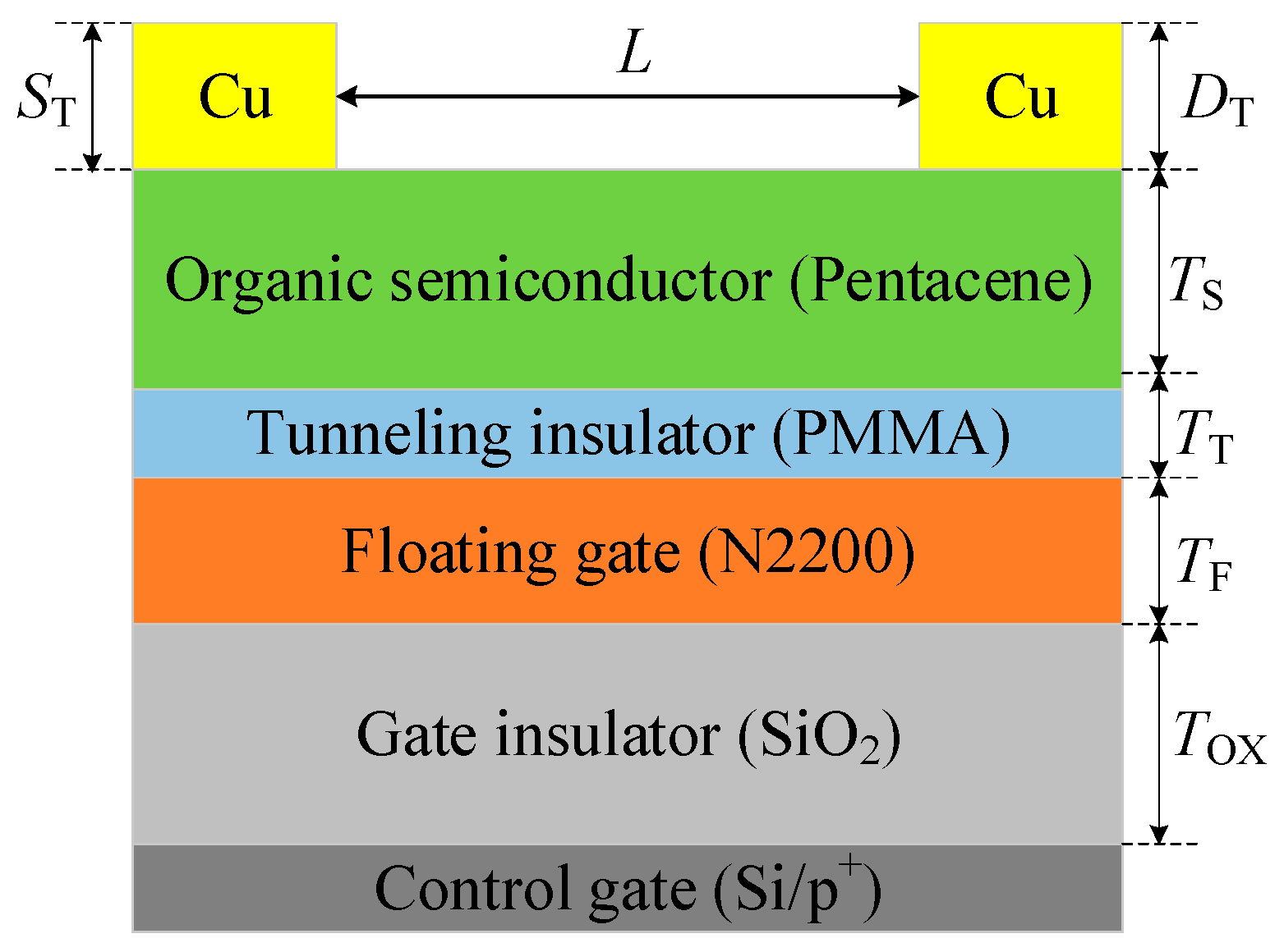
2.1. Device Structure

A bottom-gate top-contact structure is adopted by the device, as shown in Figure 1. Thermally oxidized SiO2-coated Si/p+ wafer was employed as the substrate. N2200 was spin-coated on the substrate as a floating-gate layer, PMMA was spin-coated on the N2200 surface as a tunneling layer, and pentacene was deposited on PMMA as an active layer. Finally, source–drain electrodes were deposited on pentacene using the thermal evaporation technique, and copper with a high work function was utilized as the source and drain electrodes. Refer to Figure S1 for details of the device fabrication process. Among these, PMMA can also be used as a charge-trapping layer [34]; however, in more reports in the literature, PMMA has been used as a tunneling layer in OFETM [35]. The energy level structure of PMMA makes it more suitable for functioning as a tunneling layer in this device structure. PMMA has a suitable lowest unoccupied molecular orbital energy (LUMO) level and the highest occupied molecular orbital energy (HOMO) level, which form a charge potential well in the PMMA/N2200/SiO2 structure. This ensures that the charge captured by N2200 remains for a long time. N2200 is a specific material that exhibits distinctive charge-trapping and transport properties. Compared to the materials used in previous studies, N2200 has a more suitable energy level structure, which enables it to achieve higher efficiency and selectivity in the charge-trapping process. The detailed structural and physical parameters of the device are presented in Table 1.

2.2. Physical Models

In p-channel OFETM, the carrier transport mechanism is influenced by the temperature, electric field, organic semiconductor channel, hole traps between the electrode and gate dielectric layer, etc. [36]. The carrier transport of N2200 FG-OFETM is simulated by solving the Poisson equation, the carrier continuity equation, and the hole drift diffusion equation [37,38]. The physical models employed in the experiment are as follows:
ε 0 ε S φ = q ( n p + N t P t )
J p = q ( G R )
J p = q μ p E P q D p P
D p = μ p K 0 T L q
where φ is the electrostatic potential, Nt and Pt are the density of trapped electrons and holes, respectively, and n and p are the concentrations of electrons and holes. Jp is the hole current density, G indicates the rate of hole production, which is considerably affected by the hole potential barrier, and R is the recombination rate. Ep represents the electric field strength. Dp is the hole diffusion coefficient. According to Einstein Equation (4), Jp is expressed as
J p = q μ p E P K 0 T L q P
where K0 is the Boltzmann constant, TL represents the lattice temperature (300 K), and μp is the Poole–Frenkel mobility [39].
μ p = μ P 0 exp E h 0 K 0 T + β k 0 T L γ E
In this model, μp0 represents the low-field mobility, Eh0 signifies the activation energy of the hole (E = 0) of 0.018 eV (E = 0), β is the Poole–Frenkel hole factor, and γ is the fitting parameter. In order to obtain good simulation results, the contact between the electrode and the organic semiconductor was defined as the Schottky barrier. Furthermore, the hot carrier injection and Fower–Nordheim (FN) tunneling models were used to simulate the injection of holes from the channel into the FG layer, as well as their release from the FG layer into the channel after P/E operations. The thermal emission current J and the tunneling current JFN are delineated as follows [40,41]:
J = A T 2 exp φ T q 3 E / 4 π ε 0 X K 0 T
J FN = F . AH E 2 exp F . BE E
where J and JFN are mainly influenced by E, T, and φT; φT is defined as the height of the interface barrier between the semiconductor layer and the tunneling layer (during programming) or the tunneling layer and the FG layer (during erasing); F.AH and F.BE are constants, while A* represents the Richardson constant. This research project primarily employed the mentioned physical models for numerical simulations in the investigation and analysis of FG-OFETM performance.

3. Results and Discussion

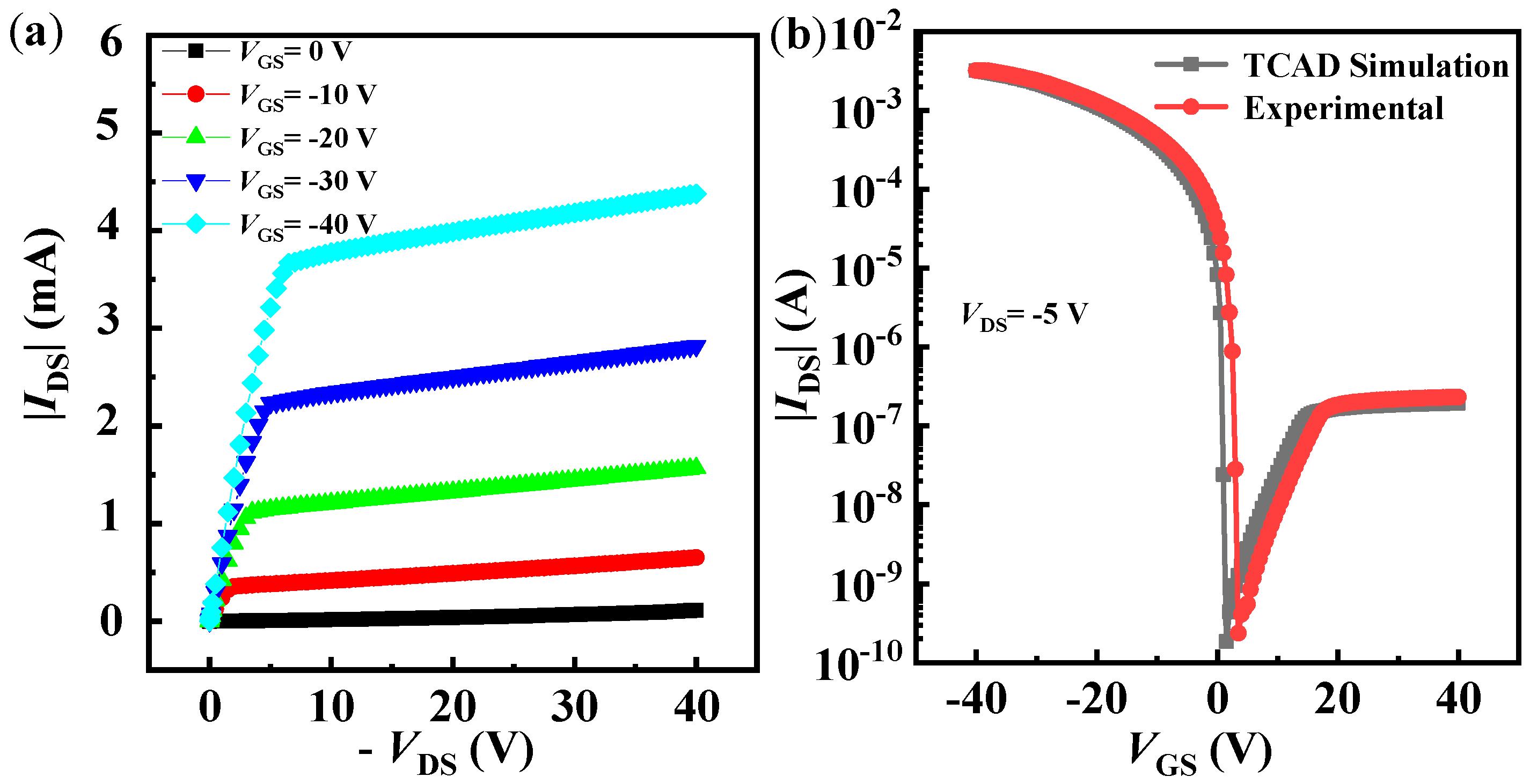
3.1. Output and Transfer Characteristics

The output and transfer characteristics of N2200 FG-OFETM are numerically simulated. The channel length of the device is 80 μm and the thickness of the tunneling layer is 8 nm, and different gate voltages are applied. The drain–source voltage (VDS) ranges from 0 V to −40 V and the gate–source voltage (VGS) from 0 V to −40 V in steps of −10 V, as shown in Figure 2a. The results show that the device exhibits typical p-channel field-effect transistor characteristics [42,43]. Figure 2b shows the initial transfer characteristic curve of the device, and the simulated transfer characteristics are in good agreement with experimental transfer characteristics. The field-effect mobility and threshold voltage (VTH) of the device are calculated by the following equations.
I DS = μ W C i 2 L V G V T V DS
where Ci is the capacitance per unit area of the device, and the channel length (L) and width (W) of the device are 80 μm and 1000 μm, respectively. The device consists of two insulating layers: the first layer is the gate insulating layer (SiO2) with a thickness of 90 nm, and the second layer is a tunneling layer (PMMA) with a thickness of 8 nm. Ci can be calculated according to the following formula [44]:
1 C i = 1 C g + 1 C t = d g ε 0 ε g + d t ε 0 ε t ,
where dg and dt are the thicknesses of the gate insulating (SiO2) and tunneling (PMMA) layers, and εg and εt are the dielectric constants of the gate insulating and tunneling layers, respectively. The calculation shows that the capacitance is 3.854 nF/cm2 and the mobility is 0.074 cm2·V−1·s−1, and the Ion/Ioff ratio exceeds 104.

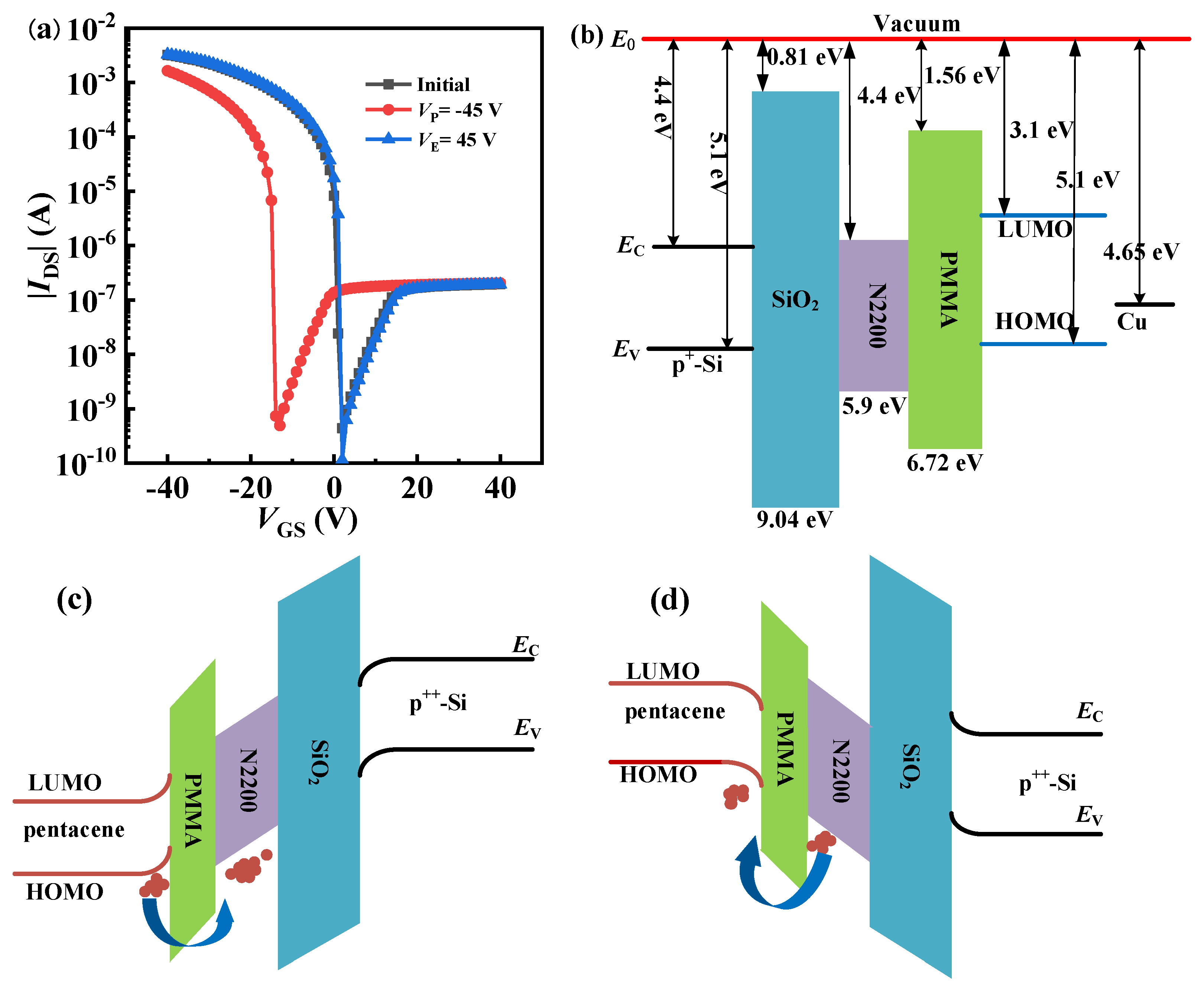
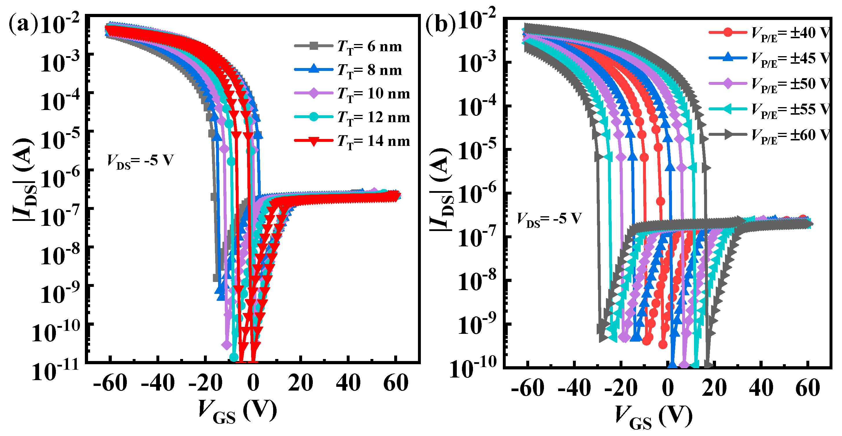
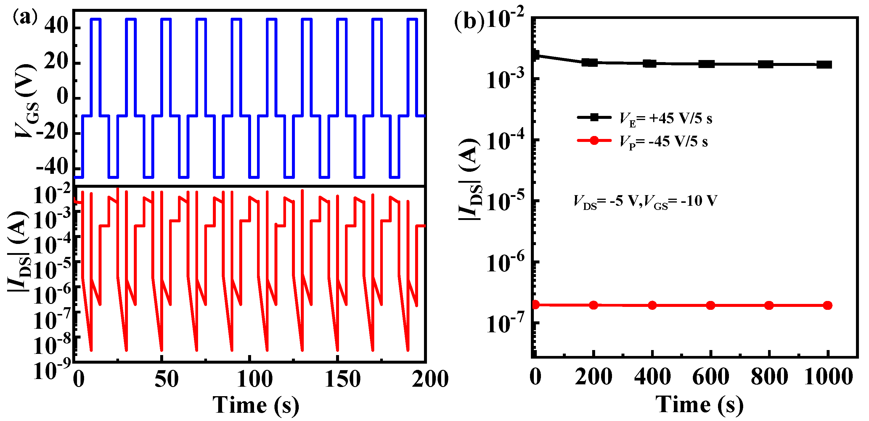
3.2. Storage Characteristics

Due to the hot charge carrier injection and FN tunneling mechanism, when a negative programming voltage is applied to FG-OFETM, the charge carriers enter the FG layer from the channel through the tunneling layer. On the other hand, when a positive erasing voltage is applied, the charge carriers captured by the FG layer are released into the channel. Both of the above-mentioned processes can lead to a shift in VTH, which enables the device to exhibit distinguishable physical states for representing the binary 0 and 1. As shown in Figure 3a, the simulated results show that the transfer characteristic of N2200 FG-OFETM has obvious negative and positive shifts under the P/E voltage of ±45 V, 5 s, and the VDS is constant at −5 V.
Figure 3b shows the energy level of N2200 FG-OFETM without the application of voltage, where E0 is the vacuum energy level, and the LUMO and HOMO levels of pentacene are 3.1 eV and 5.1 eV, respectively. In Figure 3c, when a negative gate voltage (VGS) is applied, holes are accumulated at the interface between the pentacene layer and PMMA layer; the energy band of PMMA is greatly bent, which causes holes to be injected into the N2200 FG layer from the channel. The holes captured by the FG layer generate an internal electric field in the opposite direction to the applied negative gate voltage, resulting in a negative shift in the transfer characteristic curve, which is a programming operation. Then, the positive erasing voltage is applied to the device; as shown in Figure 3d, the transfer characteristic curve is returned to the initial position. This is an erasing operation, which indicates that the holes captured by the N2200 FG layer during the programming operation are extracted back to the active layer due to the erasing operation.
The storage characteristics of N2200 FG-OFETM are closely related to factors such as the thickness of the tunneling layer, the magnitude of the operating voltage, and the operation time of P/E voltages. Firstly, the impacts of different tunneling layer thicknesses on the memory window are investigated. There are five samples with tunneling layer thicknesses of 6 nm, 8 nm, 10 nm, 12 nm, and 14 nm. Figure 4a shows that the memory windows that vary with the thickness of the tunneling layer are 24.4 V, 16.1 V, 12.1 V, 7.9 V, and 4.7 V, respectively. It can be observed that the offset of the transfer characteristic curve is the largest when the thickness of the tunneling layer is 6 nm. The memory window decreases with the increase in tunneling layer thickness, because a thinner tunneling layer allows charge carriers to be more easily captured by the FG. However, the tunneling layer should have a suitable thickness. Thicker tunneling layers could make P/E operations difficult, while thinner layers could affect the retention time of storage devices. Therefore, in the subsequent simulation, N2200 FG-OFETM with a tunneling layer thickness of 8 nm is selected as the research object.
Figure 4b,c show the various memory windows under different P/E operations. With the operating voltage changed from ±40 V to ±60 V (the operating time is uniformly 5 s), the corresponding memory windows are 12.4 V, 16.1 V, 25.9 V, 35.9 V, and 45.8 V, respectively. When VP = −45 V, the transfer characteristic curve returns to the initial position, indicating that all the holes captured by the FG layer are extracted back to the active layer after erasing. When VP/E > ±45 V, the transfer characteristic curves after erasing are on the right side of the initial position, which suggests that when the erasing voltage is increased, first, all holes in the FG layer are extracted back to the active layer, and then electrons are injected from the active layer to the FG layer and captured by the FG. This phenomenon may be explained by the hot carrier injection mechanism [30]: (1) In certain conditions, the erasing operation is more likely to occur than the programming operation. In Figure 3b, the programming process energy barrier value (1.62 eV) for holes crossing the tunneling layer is slightly higher than the erasing process energy barrier value (0.82 eV). (2) Although the electrons are minority carriers in the p-type pentacene active layer, the energy barrier value (1.54 eV) for electron transport between the LUMO level of pentacene and N2200 is lower than that (1.62 eV) for hole transport between the HOMO level of pentacene and N2200.
Furthermore, the impacts of applying different P/E operation times on the device are studied. As shown in Figure 4d, the VDS = −5 V, VP/E = ±45 V, and the P/E operation times are set at 1 s, 5 s, 10 s, and 15 s, respectively. It can be observed that the memory windows of the device rise with the increase in the P/E operation time. The time integration of the FN tunneling current density in Equation (8) shows that the longer the operation time applied is, the more charge carriers are tunneled from the active layer into the FG layer, although the magnitudes of the P/E voltages are the same. However, when the P/E operation time exceeds 5 s, the positive and negative offsets of the transfer characteristic curves do not change significantly. This phenomenon indicates that the ability of the FG to capture charges has a certain limit. The results are also consistent with those previously reported in the literature [30]. As the number of captured charges in the FG layer increases, the built-in electric field generated by the FG layer becomes stronger. The direction of the built-in electric field is opposite to the P/E electric field, which leads to a tunneling electric field decrease during P/E operation. When the actual electric field of the tunneling layer is less than the minimum electric field required for FN tunneling to occur, the charge carried in the active layer will not be further injected into the FG layer. Although the P/E operation time is increasing, the charge in the FG layer will not continue to increase. Therefore, the memory window no longer increases significantly when the P/E operation time exceeds 5 s. Table 2 summarizes the memory windows and P/E voltages of FG-OFETM with different FG layer and tunneling layer materials in the recent literature. The comparison results show that the N2200 FG-OFETM presented in this work has a relatively low P/E voltage and large memory window (VP/E = ±45 V, 5 s; memory window is 16.1 V).
Finally, the effect of temperature on the device’s performance was investigated. A series of temperature-controlled experiments were designed to test the device in different temperature ranges (40 °C, 60 °C, 80 °C, 100 °C, and 120 °C) to study the effect of temperature changes on key performance parameters such as the memory window, as shown in Figure 5. It can be seen from Figure 5a,b that temperature significantly impacts the programming characteristics of the device and has almost no effect on the erasure characteristics. When the temperature is 40 °C, the memory window of the device is largest, reaching 32.7 V. With the increase in temperature, the memory window of the device gradually decreases, and when the temperature is ≥80 °C, the transfer characteristic curve of the device no longer changes. Through these temperature stability tests, the memory performance of the device in different temperature environments can be better understood, and some references for subsequent temperature effects on device performance can be provided. Table 2 summarizes the memory windows and P/E voltages of FG-OFETM with different FG layer and tunneling layer materials in the recent literature. The comparison results show that the N2200 FG-OFETM presented in this work has a relatively low P/E voltage and large memory window (VP/E = ±45 V, 5 s; memory window is 16.1 V).
For P-type OFETM, under a certain VDS, when VGS is less than VTH, IDS is almost zero and the transistor is in the off state (IOFF). When the negative VGS exceeds VTH, a conductive channel is induced in the active layer, IDS increases rapidly, and the device is in the on state (ION). P/E operation causes VTH drift, and at the same VGS and VDS, the IDS may exhibit differences in order of magnitude. Based on the above-mentioned characteristics, the IDS of N2200 FG-OFETM with programming–read–erasing–read (PRER) cycles is investigated. The corresponding voltages are VP = −45 V, read voltage (VR) = −20 V, VE = 45 V, and VR = −20 V at a time step of 5 s. After 200 PRER cycles, the memory characteristics of the device did not change significantly, indicating that N2200 FG-OFETM exhibits exceptional erasing endurance, as shown in Figure 6a. Figure 6b displays the retention characteristics of N2200 FG-OFETM. After a P/E voltage of ±45 V, 5 s, is applied to the device, the read current on/off ratio reaches 103.

4. Conclusions

In this paper, FG-OFETM with a bottom-gate top-contact structure was designed by using the n-type semiconductor N2200 as the FG layer. Through the utilization of the carrier injection and FN tunneling models with the assistance of the TCAD simulation tool, the variations in FG-OFETM memory performance under different tunneling thicknesses, operating voltages, and pulse operation times were investigated. The results show that the memory window with a tunneling layer thickness of 8 nm is 16.1 V, and the current on/off ratio is about 104 under the P/E voltage of ±45 V, 5 s. In comparison to the FG-OFETM results reported in previous research (in Table 2), N2200 FG-OFETM can obtain a relatively larger memory window at a small operating voltage. After 200 cycles of PRER testing, the device shows good endurance to erasing and writing, and its read current on/off ratio reaches 103.

Supplementary Materials

The following supporting information can be downloaded at: https://www.mdpi.com/article/10.3390/app15052278/s1, Figure S1. Device fabrication process. Reference [48] is cited in the supplementary materials.

Author Contributions

Conceptualization, W.Z.; methodology, W.Z.; software, J.S.; validation, M.M. and D.M.; formal analysis, J.S. and S.L.; investigation, S.L. and J.S.; resources, M.M. and W.Z.; data curation, D.M.; writing—original draft preparation, W.Z. and J.S.; writing—review and editing, W.Z. and S.L.; visualization, J.S. and S.L.; supervision, M.M.; project administration, J.S. and S.L.; funding acquisition, H.L. and W.Z. All authors have read and agreed to the published version of the manuscript.

Funding

This research was funded by the Natural Science Foundation of Gansu Province (Grant No. 22JR11RA154) and the National Natural Science Foundation of China (Grant No. 62264008).

Institutional Review Board Statement

Not applicable.

Informed Consent Statement

Not applicable.

Data Availability Statement

The data presented in this study are available on request from the corresponding author. The data are not publicly available due to privacy.

Conflicts of Interest

The authors declare no conflicts of interest.

References

  1. Hu, D.; Wang, X.; Chen, H.; Guo, T. High performance flexible nonvolatile memory based on vertical organic thin film transistor. Adv. Funct. Mater. 2017, 27, 1703541. [Google Scholar] [CrossRef]
  2. Jeong, Y.J.; Yun, D.J.; Kim, S.H.; Jang, J.; Park, C.E. Photoinduced recovery of organic transistor memories with photoactive floating-gate interlayers. ACS Appl. Mater. 2017, 9, 11759–11769. [Google Scholar] [CrossRef]
  3. Zhao, Y.; Wang, W.; He, Z.; Peng, B.; Di, C.A.; Li, H. High-performance and multifunctional organic field-effect transistors. Chin. Chem. Lett. 2023, 34, 108094. [Google Scholar] [CrossRef]
  4. Chen, H.; Zhou, Y.; Han, S.T. Recent advances in metal nanoparticle-based floating gate memory. Nano Select 2021, 2, 1245–1265. [Google Scholar] [CrossRef]
  5. Kumar, S.; Kumar, A.; Mishra, R.D.; Babu, P.; Pandey, S.K.; Devi, S.; Kumar, M. Multilevel Nanophotonic Resistive Switching in Ag-ITO-SiO 2 on Silicon with Enhanced Optical Storage Density. J. Light. Technol. 2024, 43, 1299–1305. [Google Scholar] [CrossRef]
  6. Nguyen, T.H.; Imran, M.; Choi, J.; Yang, J.S. HYDRA: A Hybrid Resistance Drift Resilient Architecture for Phase Change Memory-Based Neural Network Accelerators. IEEE Trans. Comput. 2024, 73, 2123–2135. [Google Scholar] [CrossRef]
  7. Wu, H.; Chen, A.; Zhang, P.; He, H.; Nance, J.; Guo, C.; Wang, K.L. Magnetic memory driven by topological insulators. Nat. Commun. 2021, 12, 6251. [Google Scholar] [CrossRef] [PubMed]
  8. Yoo, J.; Song, H.; Lee, H.; Lim, S.; Kim, S.; Heo, K.; Bae, H. Recent research for HZO-based ferroelectric memory towards in-memory computing applications. Electronics 2023, 12, 2297. [Google Scholar] [CrossRef]
  9. Leydecker, T.; Herder, M.; Pavlica, E.; Bratina, G.; Hecht, S.; Orgiu, E.; Samorì, P. Flexible non-volatile optical memory thin-film transistor device with over 256 distinct levels based on an organic bicomponent blend. Nat. Nanotechnol. 2016, 11, 769–775. [Google Scholar] [CrossRef]
  10. Heshami, K.; England, D.G.; Humphreys, P.C.; Bustard, P.J.; Acosta, V.M.; Nunn, J.; Sussman, B.J. Quantum memories: Emerging applications and recent advances. J. Mod. Opt. 2016, 63, 2005–2028. [Google Scholar] [CrossRef]
  11. Xie, S.; Tu, L.; Han, Y.; Huang, L.; Kang, K.; Lao, K.U.; Poddar, P.; Park, C.; Muller, D.A.; Park, J. Coherent, atomically thin transition-metal dichalcogenide superlattices with engineered strain. Science 2018, 359, 1131–1136. [Google Scholar] [CrossRef] [PubMed]
  12. Chen, Y.; Yu, H.; Gong, J.; Ma, M.; Han, H.; Wei, H.; Xu, W. Artificial synapses based on nanomaterials. Nanotechnology 2018, 30, 012001. [Google Scholar] [CrossRef]
  13. Zhu, Z.; Guo, Y.; Liu, Y. Application of organic field-effect transistors in memory. Mater. Chem. Front. 2020, 4, 2845–2862. [Google Scholar] [CrossRef]
  14. Wang, S.; He, C.; Tang, J.; Lu, X.; Shen, C.; Yu, H.; Du, L.; Li, J.; Yang, R.; Shi, D.; et al. New floating gate memory with excellent retention characteristics. Adv. Electron. Mater. 2019, 5, 1800726. [Google Scholar] [CrossRef]
  15. Khan, A.I.; Keshavarzi, A.; Datta, S. The future of ferroelectric field-effect transistor technology. Nat. Electron. 2020, 3, 588–597. [Google Scholar] [CrossRef]
  16. Kim, J.; Ho, D.; Kim, I.S.; Kim, M.G.; Baeg, K.J.; Kim, C. Solution-processed flexible nonvolatile organic field-effect transistor memory using polymer electret. Org. Electron. 2021, 99, 106331. [Google Scholar] [CrossRef]
  17. He, L.; Li, E.; He, W.; Yan, Y.; Lan, S.; Yu, R.; Cheng, H.; Guo, T. Complementary of ferroelectric and floating gate structure for high performance organic nonvolatile memory. Adv. Electron. Mater. 2021, 7, 2100599. [Google Scholar] [CrossRef]
  18. Chen, Z.; Chen, S.; Jiang, T.; Chen, S.; Jia, R.; Xiao, Y.; Pan, J.; Jie, J.; Zhang, X. A floating-gate field-effect transistor memory device based on organic crystals with a built-in tunneling dielectric by a one-step growth strategy. Nanoscale 2024, 16, 3721–3728. [Google Scholar] [CrossRef]
  19. Jeong, Y.J.; Yun, D.J.; Noh, S.H.; Park, C.E.; Jang, J. Surface modification of CdSe quantum-dot floating gates for advancing light-erasable organic field-effect transistor memories. ACS Nano 2018, 12, 7701–7709. [Google Scholar] [CrossRef]
  20. Xu, T.; Fan, S.; Cao, M.; Liu, T.; Su, J. Flexible organic field-effect transistor nonvolatile memory enabling bipolar charge storage by small-molecule floating gate. Appl. Phys. Lett. 2022, 120, 073301. [Google Scholar] [CrossRef]
  21. Yu, Y.; Ma, Q.; Ling, H.; Li, W.; Ju, R.; Bian, L.; Shi, N.; Qian, Y.; Yi, M.; Xie, L.; et al. Small-molecule-based organic field-effect transistor for nonvolatile memory and artificial synapse. Adv. Funct. Mater. 2019, 29, 1904602. [Google Scholar] [CrossRef]
  22. Liu, Y.; Shao, Z.; Yu, X.; Guo, D.; Wang, S.; Bian, L.; Chen, Y.; Liu, H.; Ling, H.; Xie, L. Graphdiyne particles as nano-floating gates for high-performance nonvolatile organic field-effect transistor memory. Org. Electron. 2024, 128, 107027. [Google Scholar] [CrossRef]
  23. Gao, X.; Liu, C.H.; She, X.J.; Li, Q.L.; Liu, J.; Wang, S.D. Photon-energy-dependent light effects in organic nano-floating-gate nonvolatile memories. Org. Electron. 2014, 15, 2486–2491. [Google Scholar] [CrossRef]
  24. Che, Y.; Zhang, Y.; Cao, X.; Song, X.; Cao, M.; Dai, H.; Yang, J.; Zhang, G.; Yao, J. Low operating voltage ambipolar graphene oxide-floating-gate memory devices based on quantum dots. J. Mater. Chem. C 2016, 4, 1420–1424. [Google Scholar] [CrossRef]
  25. Li, Q.; Zhang, Y.; Yu, Y.; Chen, Z.; Jin, L.; Li, Y.; Li, T.; Yang, Y.; Zhao, H.; Li, J. Light enhanced low-voltage nonvolatile memory based on all-inorganic perovskite quantum dots. Nanotechnology 2019, 30, 37LT01. [Google Scholar] [CrossRef] [PubMed]
  26. Li, W.; Guo, F.; Ling, H.; Liu, H.; Yi, M.; Zhang, P.; Wang, W.; Xie, L.; Huang, W. Solution-processed wide-bandgap organic semiconductor nanostructures arrays for nonvolatile organic field-effect transistor memory. Small 2018, 14, 1701437. [Google Scholar] [CrossRef] [PubMed]
  27. Xu, T.; Guo, S.; Qi, W.; Li, S.; Xu, M.; Xie, W.; Wang, W. High-performance flexible organic thin-film transistor nonvolatile memory based on molecular floating-gate and pn-heterojunction channel layer. Appl. Phys. Lett. 2020, 116, 023301. [Google Scholar] [CrossRef]
  28. Shu, S.; Xu, T.; Su, J. A flexible floating-gate based organic field-effect transistor non-volatile memory based on F8BT/PMMA integrated floating-gate/tunneling layer. Phys. Scr. 2023, 98, 045402. [Google Scholar] [CrossRef]
  29. Wang, G.; Liu, X.; Wang, W. Solution processed organic transistor nonvolatile memory with a floating-gate of carbon nanotubes. IEEE Electron Device Lett. 2017, 39, 111–114. [Google Scholar] [CrossRef]
  30. Yan, Z.W.; Wang, J.; Qiao, J.L.; Chen, W.J.; Yang, P.; Xiao, T.; Yang, J.H. Numerical simulation study of organic nonvolatile memory with polysilicon floating gate. Chin. Phys. B 2016, 25, 067102. [Google Scholar] [CrossRef]
  31. Liu, L.; Su, Y.; Xu, J.P.; Zhang, Y.X. Fabrication and Characteristics of Nano-Floating Gate Memories with ZnO Nano-Crystals as Charge-Storage Layer. Chin. Phys. Lett. 2018, 35, 068101. [Google Scholar] [CrossRef]
  32. Kim, H.R.; Kang, C.S.; Kim, S.K.; Byun, C.W.; Yoon, S.M. Characterization on the operation stability of mechanically flexible memory thin-film transistors using engineered ZnO charge-trap layers. J. Phys. D Appl. Phys. 2019, 52, 325106. [Google Scholar] [CrossRef]
  33. Yu, T.; Hou, S.; Liu, Z.; Wang, Y.; Yin, J.; Gao, X.; Liu, N.; Yuan, G.; Wu, L.; Xia, Y.; et al. Enhanced Performance of Organic Field-Effect Transistor with Bi-Functional N-Type Organic Semiconductor Layer. Adv. Electron. Mater. 2024, 10, 2300651. [Google Scholar] [CrossRef]
  34. Li, W.; Yi, M.; Ling, H.; Guo, F.; Wang, T.; Yang, T.; Xie, L.H.; Huang, W. Analysis of temperature-dependent electrical transport properties of nonvolatile organic field-effect transistor memories based on PMMA film as charge trapping layer. J. Phys. D Appl. Phys. 2016, 49, 125104. [Google Scholar] [CrossRef]
  35. Wang, W.; Han, J.; Ying, J.; Xiang, L.; Xie, W. Effect of tunneling layers on the performances of floating-gate based organic thin-film transistor nonvolatile memories. Appl. Phys. Lett. 2014, 105, 123303. [Google Scholar] [CrossRef]
  36. Mittal, P.; Yadav, S.; Negi, S. Advancements for organic thin film transistors: Structures, materials, performance parameters, influencing factors, models, fabrication, reliability and applications. Mater. Sci. Semicond. Process. 2021, 133, 105975. [Google Scholar] [CrossRef]
  37. Delavari, N.; Tybrandt, K.; Berggren, M.; Piro, B.; Noël, V.; Mattana, G.; Zozoulenko, I. Nernst–Planck–Poisson analysis of electrolyte-gated organic field-effect transistors. J. Phys. D Appl. Phys. 2021, 54, 415101. [Google Scholar] [CrossRef]
  38. Jung, S.; Bonnassieux, Y.; Horowitz, G.; Jung, S.; Iñiguez, B.; Kim, C.H. Advances in compact modeling of organic field-effect transistors. IEEE J. Electron Devices Soc. 2020, 8, 1404–1415. [Google Scholar] [CrossRef]
  39. Gill, W.D. Drift mobilities in amorphous charge-transfer complexes of trinitrofluorenone and poly-n-vinylcarbazole. J. Appl. Phys. 1972, 43, 5033–5040. [Google Scholar] [CrossRef]
  40. Matsumura, M.; Akai, T.; Saito, M.; Kimura, T. Height of the energy barrier existing between cathodes and hydroxyquinoline–aluminum complex of organic electroluminescence devices. J. Appl. phys. 1996, 79, 264–268. [Google Scholar] [CrossRef]
  41. Parker, I.D. Carrier tunneling and device characteristics in polymer light-emitting diodes. J. Appl. Phys. 1994, 75, 1656–1666. [Google Scholar] [CrossRef]
  42. Li, W.; Zhang, P.; Li, H.; Sheng, X.; Li, Y.; Xu, X.; Yi, M.; Shi, N.; Shi, W.; Xie, L.; et al. A tricolour photodetecting memory device based on lead sulfide colloidal quantum dots floating gate. Org. Electron. 2019, 75, 105111. [Google Scholar] [CrossRef]
  43. Zhang, P.; Chen, X.; Li, W.; Ling, H.; Wang, W.; Zhang, G.; Yi, M.; Xie, L.; Shi, W.; Shi, N.; et al. Organic non-volatile memory based on pentacene/tris (8-hydroxy quinoline) aluminum heterojunction transistor. Org. Electron. 2018, 57, 335–340. [Google Scholar] [CrossRef]
  44. Lamport, Z.A.; Haneef, H.F.; Anand, S.; Waldrip, M.; Jurchescu, O.D. Tutorial: Organic field-effect transistors: Materials, structure and operation. J. Appl. Phys. 2018, 124, 071101. [Google Scholar] [CrossRef]
  45. Yi, M.; Shu, J.; Wang, Y.; Ling, H.; Song, C.; Li, W.; Xie, L.; Huang, W. The effect of porous structure of PMMA tunneling dielectric layer on the performance of nonvolatile floating-gate organic field-effect transistor memory devices. Org. Electron. 2016, 33, 95–101. [Google Scholar] [CrossRef]
  46. Zhang, W.T.; Wang, F.X.; Li, Y.M.; Guo, X.X.; Yang, J.H. Organic field-effect transistor floating-gate memory using polysilicon as charge trapping layer. Chin. Phys. B 2019, 28, 086801. [Google Scholar] [CrossRef]
  47. Xu, T.; Guo, S.; Xu, M.; Li, S.; Xie, W.; Wang, W. Organic transistor nonvolatile memory with an integrated molecular floating-gate/tunneling layer. Appl. Phys. Lett. 2018, 113, 243301. [Google Scholar] [CrossRef]
  48. Wang, Y.; Kang, L.; Liu, Z.; Wan, Z.; Yin, J.; Gao, X.; Xia, Y.; Liu, Z. Enhancement of memory properties of pentacene field-effect transistor by the reconstruction of an inner vertical electric field with an n-type semiconductor interlayer. ACS Appl. Mater. Interfaces 2021, 13, 13452–13458. [Google Scholar] [CrossRef]
Figure 1. Schematic diagram of device structure.
Applsci 15 02278 g001
Figure 2. (a) Output characteristics and (b) transfer characteristics of N2200 FG-OFETM with tunneling layer of 8 nm.
Applsci 15 02278 g002
Figure 3. (a) Transfer characteristics after P/E operation, VP/E = ±45 V, 5 s; (b) energy level diagram of N2200 FG-OFETM without application of voltage; (c) energy band diagram during P operation; (d) energy band diagram during E operation.
Applsci 15 02278 g003
Figure 4. (a) Memory windows of N2200 FG-OFETM with different thickness of tunneling layer; (b,c) memory windows with different P/E voltages (tunneling layer is 8 nm); (d) memory windows under VP/E = ±45 V: operation times are 1 s, 5 s, 10 s, and 15 s, respectively.
Applsci 15 02278 g004aApplsci 15 02278 g004b
Figure 5. Changes in the test transfer characteristic curve at different temperatures. (a) Programming; (b) erasing.
Applsci 15 02278 g005
Figure 6. (a) PRER cycling test of N2200 FG-OFETM; (b) the drain currents of the ON state and OFF state after erasing and programming.
Applsci 15 02278 g006
Table 1. Physical and structural parameters used for device simulation.
ParameterSymbolValue
Channel lengthL/μm80
Channel widthW/μm1000
Thickness of source and drain electrodesST, DT/nm50
Thickness of organic semiconductorTS/nm40
Thickness of tunneling insulatorTT/nm6, 8, 10, 12, 14
Thickness of FGTF/nm18
Thickness of gate insulatorTOX/nm90
Dielectric constant of gate insulator (PMMA)εS3.0
Dielectric constant of FG layer (N2200)εS3.5
Work function (Cu)WF/eV4.65~4.70
Active layer band gap width (pentacene)Eg/eV1.8~2.2
Band gap width of FG layer (N2200)Eg/eV3.3~3.6
Table 2. Comparison of FG-OFETM performance of different FG layer materials.
FG LayerTunneling LayerVP/VE (V)Memory Window (V)Reference
Gold nanoparticlesPMMA+80/−15043[45]
Single-walled carbon nanotubesPMMA+60/−6026.7[29]
PolysiliconPMMA+60/−609.28[46]
F8BTPMMA+40/−409.28[28]
C60TTC+40/−408.0[47]
N2200PMMA+45/−4516.1This work
Disclaimer/Publisher’s Note: The statements, opinions and data contained in all publications are solely those of the individual author(s) and contributor(s) and not of MDPI and/or the editor(s). MDPI and/or the editor(s) disclaim responsibility for any injury to people or property resulting from any ideas, methods, instructions or products referred to in the content.

