Article

A Method for Grading Failure Rates Within the Dynamic Effective Space of Integrated Circuits After Testing

1
School of Electronic Engineering & Intelligent Manufacturing, Anqing Normal University, Anqing 246133, China
2
Graduate School of Computer Science and Systems Engineering, Kyushu Institute of Technology, Iizuka-shi 820-8502, Japan
*
Author to whom correspondence should be addressed.
Appl. Sci. 2025, 15(4), 2009; https://doi.org/10.3390/app15042009
Submission received: 5 November 2024 / Revised: 24 January 2025 / Accepted: 12 February 2025 / Published: 14 February 2025

Abstract

:
Integrated circuits that pass testing still have quality differences, thus making grading necessary. Traditional grading methods rely on static testing and electrical measurements, which are challenging to achieve precise grading, time-consuming, and costly. A new grading method based on the failure rate within a dynamically effective space is proposed. This method dynamically adjusts the evaluation space and uses an exponential decay function to calculate the influence weight of each neighboring chip on the evaluated chip, thereby computing the weighted failure rate of the evaluated chip and quantitatively grading the chips after wafer testing based on the scores. Experiments show that this method not only accurately captures quality differences and ensures grading accuracy but also significantly improves grading efficiency.

1. Introduction

In the semiconductor manufacturing industry, chip testing directly affects the quality and reliability of final products [1]. Each chip must pass through rigorous electrical characteristics tests, including probe testing and functional testing [2], in order to ensure the chip meets the predetermined performance standards before entering the market. In addition to traditional testing methods, the semiconductor testing field has begun to adopt cutting-edge technologies such as quantum dot testing and electromagnetic characteristic analysis [3]. These technologies aim to explore the micro-level electrical characteristics and failure modes of chips. The development of Automatic Test Equipment (ATE) [4] has significantly facilitated the implementation of large-scale chip testing, which continues to expand its operation spheres to include higher speeds, larger ranges, and lower costs. This implementation has moved at superhigh speeds, increasing testing efficiency and coverage, and decreasing the false negatives and false positives. At the same time, the application of artificial intelligence and machine learning has enhanced the optimization of testing processes and the precision of defect detection [5]. The establishment and implementation of international standards such as IEEE 1149.1 (JTAG) [6] have provided a uniform and standardized framework for global chip testing practices. With the emergence of technologies like IoT, 5G communications, and AI, chip testing has welcomed new opportunities and challenges, leading to innovative developments in testing technologies that improve and ensure quality assurance in chip design and manufacturing [7].
Chip testing not only helps to identify and eliminate defective chips but also provides the basis for chip grading [8]. Although chips that have passed basic quality control still pose a failure risk, this risk is often related to the chip’s performance stability under different working conditions [9,10]. Through refined grading, manufacturers can optimize resource allocation by using high-performance chips for applications with stringent requirements and assigning lower-performance chips to other applications which are sensitive to cost [11]. This strategy not only optimizes resource use and enhances the market competitiveness of product lines [12], but it also reduces potential safety issues caused by chip failures. Chip grading serves not only advancing technology but also controlling costs [13,14], thereby impacting competitiveness.
With the pace of development within the industry, it has become overwhelmed with chip design and manufacturing, with rising demands for grading and quality control. Traditional chip grading methods rely on static testing and electrical measurements [15], which are increasingly inefficient in rapidly changing production lines, often resulting in the inaccurate characterization of minute performance differences. This ultimately leads to incorrect grading, raising the cost of high-density integrated circuits and high-performance chips [16]. Additionally, traditional testing equipment is physically limited in sensitivity and accuracy, so it cannot catch the very subtle instances of incorrect grading, which in turn negatively influences the accuracy and trustworthiness of the grading [17]. As a result, unified testing standards can no longer meet the needs of modern high-performance, high-reliability integrated circuits [18,19].
To accommodate the increasingly complex designs and production demands of integrated circuits, manufacturers and research institutions are adopting a variety of cutting-edge technologies and methods to improve the accuracy and efficiency with which chips can be graded [20]. Dynamic testing technologies enable more comprehensive performance evaluations under simulated real-world conditions [21], examining basic electrical characteristics, analyzing long-term variability, and investigating failure modes. Alongside such advanced techniques, artificial intelligence and machine learning are extensively used for testing data analysis, where training from historical data allows for the automatic identification of performance issues or potential derivatives. These innovations not only advance the sophistication of chip grading but also improve its practicality [22], helping manufacturers meet market demands for high-performance and highly reliable chips.
Domestic companies, such as SMIC and Huahong Semiconductor [23], are developing more advanced grading technologies using machine learning and artificial intelligence algorithms, increasing grading accuracy and data processing capabilities. This system has increased automation and processing, which has consequently raised operating and maintenance costs owing to its complexity and skill requirements [24]. Hai Guang Integrated Circuit Design Company [12] proposed a dynamic adjustment grading method where the final test result of packaged chips can be used as a grading scale. The method thus developed gives a good accuracy as well as consistency in grading by packaging and testing bare dies, but this also leads to increased complexity and testing time in the systems [25].
In the US, Europe, and Japan, companies such as Intel, Samsung, and TSMC use highly automated and integrated testing systems [11]. These include 3D X-ray microscopy, automated defect detection, high-speed electrical testing, and advanced image processing technologies that thoroughly characterize and classify chips [26]. Winbond uses sample classification methods to significantly reduce testing time, at the cost of compromising comprehensiveness. TSMC employs PCA-based methods that aim to optimize yield analysis and improve data-processing efficiency [27], although this requires complex data support. While grading precision and efficiency have indeed been very much improved via these techniques, their general uptake has been hampered because of high costs and technical complexity.
Against this backdrop, researchers have introduced artificial intelligence algorithms, combined with traditional testing methods, for efficient chip grading [28]. The Parameter Parts Average Testing (PPAT) combined with Statistical Yield Analysis (SYA) allowed the real-time analysis of the defects present and dynamic adjustments to made to the allocation of resources in tests to optimize testing [29,30]. By combining PPAT and SYA with artificial intelligence algorithms, it can optimize the allocation of testing resources, ensuring product quality and reliability.
Additionally, regional PAT improves the stringency of product quality control by evaluating the proximity weights of bare dies and eliminating good bare dies around failed ones [31,32]. However, these methods still have deficiencies in dynamic adjustments and real-time environmental adaptation, thus making it difficult to cope with inherent process variations and outlier occurrences during production.
Traditional grading systems are riddled with excessive rigidity and poor accuracy. Existing machine learning and artificial intelligence algorithms show great dependence on extensive historical data that are not often available for real-time environments [33,34,35]. To tackle these setbacks, this paper proposes an innovative method for grading chips where grading is based on failure rates within a dynamically effective space and the effect of nearby chips is assessed through weighted failure rate, which autonomously modifies the grading span and precludes grading errors that had previously resulted from using the traditional method.
It also uses an exponential decay function to avoid the interference of extreme values, as well as having the ability to dynamically adjust the failure rates of neighboring areas, which can more accurately handle the dies at the wafer edges. Compared with existing machine learning-based chip grading methods, the proposed method does not rely on complicated data processing and training data steps, reflecting the characteristics of high accuracy and low resource consumption.
Although chips after wafer-level testing may still have failure risks, this grading method can effectively distinguish chip grades, reducing potential risks in subsequent applications. This method is suitable for high performance chip production and can reduce resource waste caused by inaccurate grading.
To clarify the terminology, we use “die” to specifically refer to individual, unpackaged chips on the wafer, while “chip” is used as a general term that can refer to both packaged and unpackaged semiconductor components. For simplicity and readability, the term “chip” is retained throughout the text, but in the context of wafer-level testing, it refers to dies. The abbreviations used in the algorithms are listed in Table A1 in Appendix A, while those used in the experiments and introduction are listed in Table A2 in Appendix A.

2. Algorithm Description

This paper uses the fault rate around the evaluated die (chip) as the main evaluation criterion and utilizes other test parameters’ proximity to their specified standards during the testing phase as auxiliary criteria. By calculating the weighted normalized values of both, the evaluated die is given a comprehensive score for subsequent grading. The specific process is shown in Figure 1.

2.1. Calculate the Failure Rate of the Evaluated Die

Calculating the failure rate of a die first requires determining its evaluation range. The evaluation of each die begins by defining its evaluation space, which is dynamically adjusted based on the failure rates of neighboring dies.

2.1.1. Determination of Effective Space

  • Processing of evaluated dies with sufficient number of surrounding dies
    • Set a minimum radius (r = 3) as the initial radius and calculate the failure rate within the current radius:
      Fault Rate = Number of Faulty Dies within r Total Number of Dies within r ,
      where the “Number of Faulty Dies within r” is the number of faulty dies within the current radius, and the “Total Number of Dies within r” is the total number of dies within the current radius.
    • Set a maximum threshold R and dynamically adjust the evaluation radius until the final radius is obtained:
      Within the range of r = 3 , if the Fault Rate is less than 1 3 , expand the radius to r + 1 . If the Fault Rate is still less than 1 3 when the evaluation radius is 4, then extend it to r + 3 , choosing r = 7 as the final radius (if the maximum range of the evaluated die is less than 7, choose the current r as the final r).
      In the range where r = 3 , if the Fault Rate is less than 1 3 , expand the radius to r + 1 , meaning that the evaluated radius is 4; if it exceeds 1 3 , expand r outward three times, while each time the Fault Rate is less than 1 3 , select this time r for subsequent calculation. If the Fault Rate is greater than 1 3 , expand r outward three times, and each time, if the Fault Rate is greater than 1 3 total, select r + 3 for subsequent calculation.
      Otherwise, extend to r = R .
  • Processing of edge parts
    During the expansion of the radius, it is necessary to evaluate whether the number of dies within the current radius is sufficient to determine if there are missing dies in certain directions or if the evaluated die is located at the edge of the wafer. For dies located at the edge of the wafer and missing dies in certain directions, the average failure rate of neighboring points is used as virtual data to estimate the average failure rate of a missing part.
    • Starting from radius 1, gradually check the actual number of neighboring dies within each radius range. If the data in a certain direction of the edge die are insufficient, calculate the average failure rate (afr) of the currently available neighboring die radius range:
      afr = Σ failure state of actual adjacent die the number of actual adjacent dies ,
    • Dynamically adjust the radius and fill in data. Dynamically calculate and update the average failure rate of neighboring dies according to the evaluation radius at each step. Each time the evaluation radius is expanded, recalculate the average failure rate of all actual neighboring dies within that radius and use these data to fill in the virtual neighboring dies.
    • If sufficient neighboring die data are already included within a certain radius range, or further expansion of the radius does not add new actual neighboring dies, expand and judge according to the above steps, determine the final evaluation space, and fill in the missing die data for different radius.

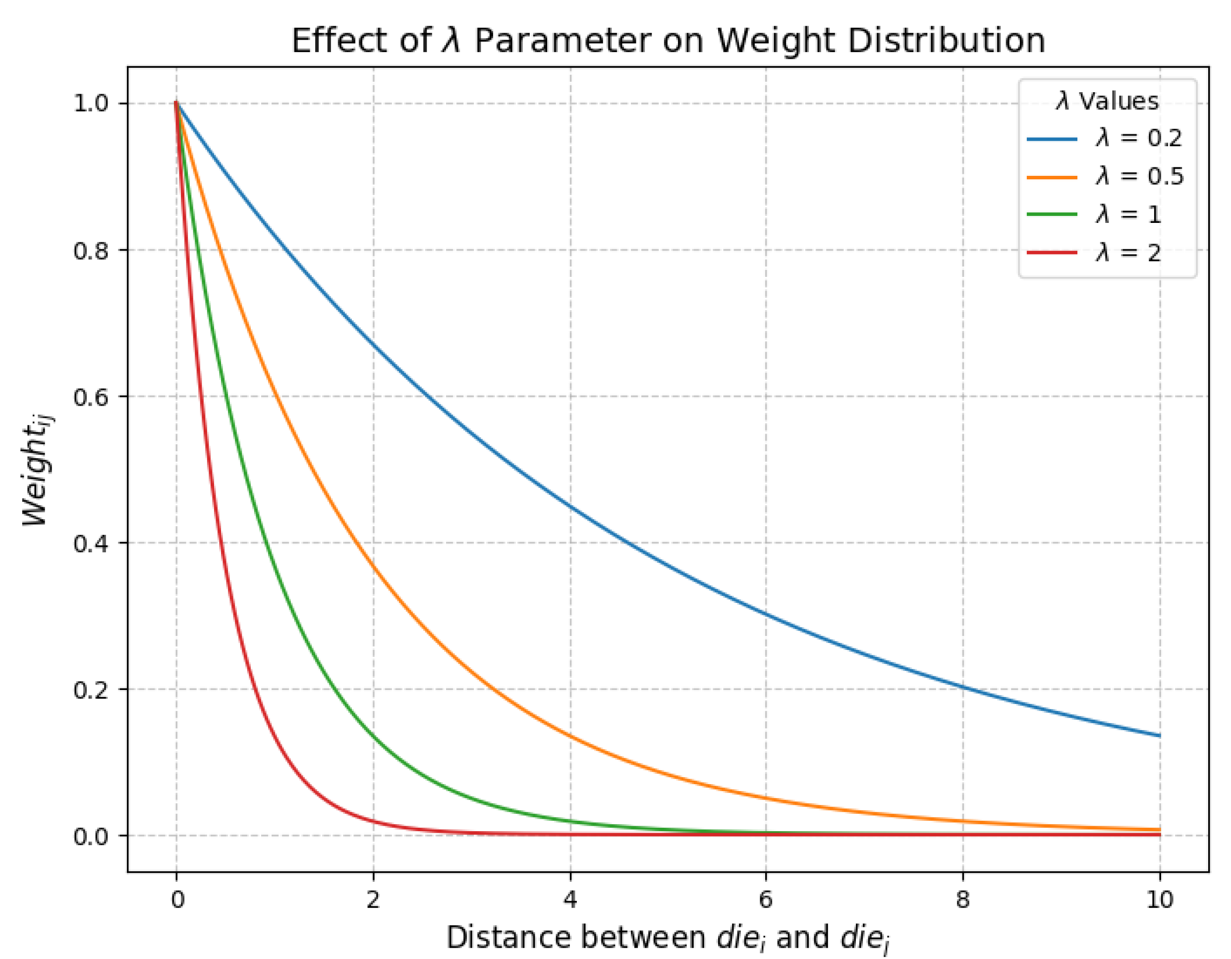
2.1.2. Calculate Impact Weight

On a wafer, regional failures may affect the reliability of surrounding chips. The degree of impact varies according to the different distances between the failed chip and the evaluated chip, The closer a faulty die is to the die under evaluation, the greater its impact. Calculate the influence weight of each chip within the final evaluation space on the evaluated chip using the following exponential decay function:
Weight i j = e λ d i j ,
where the d i j is the distance from die i be evaluated to the neighborhood die j , and λ is the attenuation coefficient for controlling the decay rate of the influence.
The exponential decay function provides a smooth and continuous way to reduce the influence of other dies they are farther from the evaluation center die. When the value of λ increases, the Weight i j decreases. Figure 2 shows how different λ values (e.g., λ = 0.2, 0.5, 1, 2) affect Weight i j , where the horizontal axis represents the distance between die j and die i , and the vertical axis represents the Weight i j . According to Figure 2, smaller λ values result in slower weight decay, making the impact of farther dies on the evaluated die more significant and applicable to a larger evaluation range. However, this may also introduce some irrelevant interference; larger λ values cause rapid weight decay, and the influence of nearby dies is more significant, which can avoid interference from distant dies and is suitable for the accurate classification of local ranges.

2.1.3. Calculation of Final Weighted Failure Rate

Each die has two states: normal (marked as 1) and failed (marked as 0). After determining the evaluation range, perform a weighted calculation of the failure rates of all dies within its range to obtain the weighted failure rate (wfr) of the evaluated die:
wfr i = j neighbors ( Weight i j × state j ) j neighbors Weight i j ,
where the state j is the state of die j , with 0 for failure and 1 otherwise. The denominator is the sum of the weights, ensuring that the score is calculated based on relative rather than absolute failure impact. This makes it possible to more fairly assess the influence of neighboring die failures on the central die, while taking distance into account.

2.2. Performance Evaluation by Parameters

During the wafer testing phase, there are a lot of test data for each evaluated die. The score for each test item needs to be calculated based on the test results of these test parameters and their proximity to the upper and lower limits of the test items. The closer the test value is to the specified range, the higher the score.

2.2.1. Calculation of the Score of Each Parameter Item

Calculate the score for each test item k:
P_score k = 1 min ( | test_value k uplimit k | , | test_value k downlimit k | ) uplimit k downlimit k ,
where the P_score k is the score of k, test_value k is the test result of a certain k test item of the evaluated die, and uplimit k and downlimit k are the specified ranges of this test item, respectively.

2.2.2. Calculation of the Test Total Score of the Test Item

After obtaining the scores of each parameter item, perform weighting and normalization to ensure that all scores reasonably reflect the test total score:
test_total_score i = all k P_weight k × P_score k all k P_weight k × P_score k ,
where P_weight k highlights the relative importance of different test items.

2.3. Rank Division

2.3.1. Calculation of the Total Score

Combine the weighted failure rates derived from the influence of all neighboring die failures with the test total scores, and multiply each by its corresponding weighting factor to calculate a comprehensive score as follows:
Score i = w 1 × wfr i + w 2 × test_total_score i .
where w 1 and w 2 are the weights. In practice, w 2 is less than w 1 . w 1 and w 2 are used to adjust the influence of the weighted failure rate and test phase score on the total score.

2.3.2. Result Optimization

To achieve consistency in the magnitude and improve the generality of the model to make it more robust to input data of different magnitudes or units and to allow the scoring system to be more widely applicable to different evaluation environments and standards, perform normalization on the results as follows:
final_score i = Score i min ( Score ) max ( Score ) min ( Score ) .

2.3.3. Grade Definition

Based on the final normalized total score and using the standard deviation method, the deviation of each die from the average level of the entire batch is assessed to ensure quality consistency.
  • Calculate the average score of all dies.
  • Calculate the standard deviation of the scores.
  • Set multiple quality levels as shown in Table 1:
Where Average refers to the average score, and “SD” denotes the standard deviation. Apply the above criteria to each die and classify it into the corresponding quality grade.

3. Experimental Procedure

This experiment was based on a real production dataset containing the test results and status information of thousands of chips.

3.1. Description of the Data Set

In this experiment, the data are divided into three parts: metadata, headers, and data.
The metadata part mainly includes the following information: test program path (Test_Program), the specific batch being tested (Lot_ID), operator identifier (Operator), specific test identifier (Test_ID), and the date and time of the test (Date).
The headers section includes the upper limit for each measurement item (UpLimit), the lower limit for each measurement item (DownLimit), and the unit for each measurement parameter (Unit).
The measurement data mainly include the following information: the serial number of the test item (Serial), the test site number (Site), the X coordinate of the probe (ProbeX), the Y coordinate of the probe (ProbeY), and other columns representing specific measurement parameters (such as OSN_TCK(V), IDD(A), LDO(V), etc.) along with their respective units and recorded values.

3.2. Data Cleaning

In this experiment, in order to ensure the accuracy of the data used, the raw data were obtained from a CSV file, the chip test data were read using the Python’s Pandas library for reading the CSV file, and the data were loaded into a DataFrame, detect, filter, and mark missing values, outliers, and format inconsistencies. The preliminary cleaning of data by using python scripts was undertaken to remove any outliers or missing data. The data format was standardized to ensure that all data items met the analysis requirements.
The table structure was defined using the DB Browser for SQLite and the cleaned data were imported into the table using Pandas. During the experiment, to simplify operations and ensure data relevance, specific columns were selected from the raw data. These columns include the unique identifier of the chip (Serial), the coordinates of the chip on the wafer (ProbeX, ProbeY), and the test results of certain parameters and their upper and lower limits, which are stored in the table.
At the same time, based on the raw data, the table structure was defined with the addition of four extra fields: state for storing the chip status, failure_rate_score for the weighted failure rate score, test_data_score for the test item score, total_score for the total score, and grade for the final grade.

3.3. Specific Experimental Procedure

Before the experiment, the status of each chip was determined from the database based on its test results and upper and lower limits, and chips were marked as normal (STATE = 1) or failed (STATE = 0). The experiment created three scripts to calculate the weighted failure rate score ( wfr i ), parameter item score ( test_total_score i ), total score ( final_score i ), and grade evaluation, respectively. For the weighted failure rate score, the evaluation space was dynamically adjusted, the evaluation range was determined, the influence weights were calculated to obtain the weighted failure rate, and the average failure rate of neighboring chips was used as virtual data to supplement chips with insufficient data in the evaluation space. The parameter item scores were combined to obtain the total score, grade classification was performed, the database data were updated, and the csv file was exported.

3.4. Experiment for Comparison

To verify the effectiveness of the proposed chip grading method based on failure rates within a dynamically effective space, we compared it with the traditional electrical testing grading method. The specific steps are as follows:
  • Use other parameter items in the wafer test for calculation to obtain the test item scores for each chip (the parameter item OSN_DCIN was selected for this experiment).
  • Calculate the total score for each chip and perform grade classification, and save the results to the database (Grade_Test).
  • A comparative analysis of the results was made: compare the grading results of this method (Grade) with the traditional method (Grade_Test), and calculate the accuracy and confusion matrix to evaluate the performance of both methods.
    • Obtain Grade and Grade_Test column data from the database.
    • Accuracy calculation: Use the accuracy_score function in sklearn.metrics to calculate the accuracy of Grade and Grade_Test, evaluating the grading accuracy of this method compared to the traditional method.
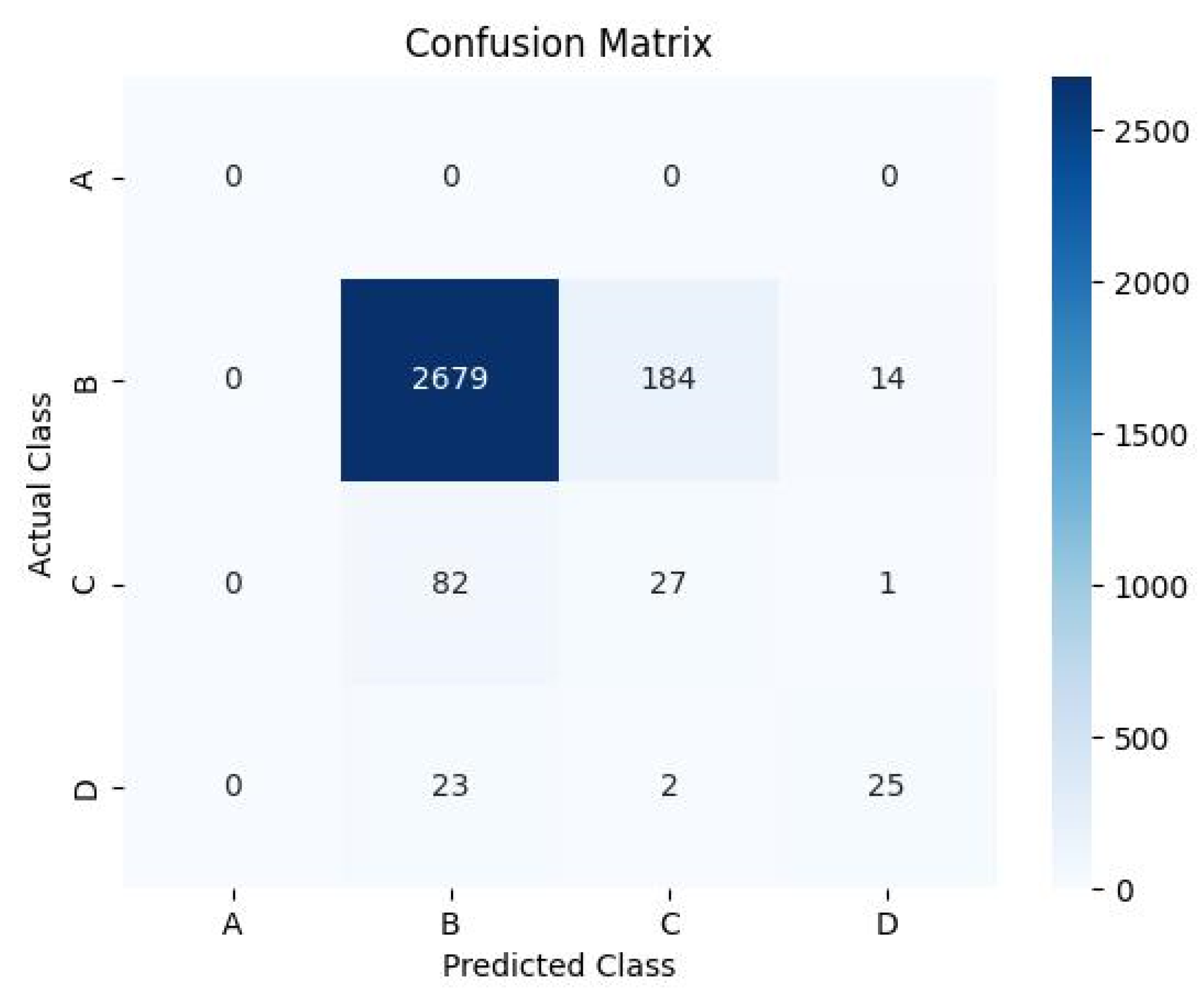
    • Calculation of confusion matrix: Use the confusion_matrix function in sklearn. metrics to calculate the confusion matrix of Grade and Grade_Test, analyzing the classification performance for each category (A, B, C, D).
    • Analyze and interpret the results: Calculate precision, recall, and F1 scores to show the model’s performance in each category.
Through the above experimental steps and results analysis, the feasibility and effectiveness of the grading method proposed in this paper were systematically evaluated in practical applications, and the results were compared compare it with traditional method for verification.

3.5. Experimental Result

3.5.1. Partial Experimental Results

Some experimental results are shown in Table 2, where the W_score is the weighted failure rate of the evaluated chip, the T_score is the parameter item score of the evaluated chip, and the F_score is the total score.

3.5.2. Comparative Experimental Results

The confusion matrix generated by the comparison experiment is shown in Table 3, and its heatmap is shown in Figure 3, illustrating the performance of the proposed chip grading method based on failure rates within a dynamically effective space across various categories. The specific analysis is as follows:
  • Accuracy: 0.899, indicating that 89.9% of the samples in all test samples were correctly classified by this method.
  • Each piece of data of the confusion matrix represents the classification between different categories, which is explained as follows:
    • First row (samples with actual category A): No actual category A samples were correctly or incorrectly classified (all values are 0).
    • Second row (samples with actual category B): 2679 actual category B samples were correctly classified as B. A total of 184 actual category B samples were incorrectly classified as C. A total of 14 actual category B samples were incorrectly classified as D.
    • Third row (samples with actual category C): 82 actual category C samples were correctly classified as B. One actual category C sample was incorrectly classified as D.
    • Fourth row (samples with actual category D): 23 actual category D samples were correctly classified as B. Two actual category D samples were incorrectly classified as C.
Performance metrics by category are shown in Figure 4, demonstrating the performance of the classification model in four categories (A, B, C, D). The blue line represents precision, showing the proportion of samples predicted as the category by the model that are actually in that category; the green line represents recall, showing the proportion of all samples actually in that category that are correctly predicted by the model; the red line represents the F1 score, which is the harmonic mean of precision and recall, used to measure the overall performance of the model.
The comparison experiment shows that the proposed grading method achieves an accuracy of 89.9%, indicating that it can correctly classify chips in most cases with high accuracy.

3.5.3. Algorithm Comparison

Memory and time consumption tests and robustness tests were conducted for the grading method using failure rates within a dynamically effective space and the grading method relying on traditional electrical testing. The memory and time usage of the two algorithms are shown in Table 4, and the robustness test results are shown in Figure 5.
In actual production environments, the chip testing process may be affected by various random disturbances, such as instrument measurement errors, environmental interference, and noise during signal transmission. To validate the robustness of the proposed method under different noise levels, Gaussian noise was artificially introduced to simulate potential random disturbances. The level of noise is represented by the standard deviation σ , ranging from 0 to 8, simulating different noise environments. By adding random noise to the measured values of chip testing items, the instability of testing equipment and environmental interference can be simulated.
Figure 5 shows the grading results of the proposed method and traditional method at different noise levels. The proposed method (blue curve) shows almost no change with increasing noise levels, while the traditional method (orange curve) exhibits sensitivity to noise, indicating its susceptibility to random interference.
In terms of time and memory consumption, the average processing time of the proposed method is 0.69 s, while the traditional method is 1.52 s, which reduces time consumption by 54.6%. The proposed method uses 62.88 MiB of memory, which is 1.6% less than traditional method. Moreover, the proposed method has good robustness, which can provide more reliable results under complex production conditions.
In conclusion, the proposed algorithm can optimize memory usage, reduce computation and resource consumption while ensuring grading accuracy, and its good stability is suitable for production environments that require efficient processing of large-scale chip data.

4. Conclusions

This paper proposes a chip grading method based on weighted failure rates within an effective space, which improves the accuracy in chip grading, reduces testing time and costs, and provides a suitable, economical way to grade chips in the semiconductor industry. By introducing failure rates within a dynamically effective space and combining weighted failure rates with the exponential decay functions, the proposed method enhances the accuracy of evaluating chip performance and reliability, making it a novel solution for the semiconductor domain. Dynamically adjusting the evaluation space and filling in missing data parts could enhance grading accuracy, especially for chips on the edge. The proposed method is characterized by its capability to adapt to varying testing ambient conditions and diverse performance criteria for chips, thus making it suitable for the production of high-density and high-performance chips.
Future research can introduce more environmental variables, chip characteristics, and multidimensional data to increase the accuracy and applicability of the evaluation. Furthermore, adding advanced machine learning and artificial intelligence algorithms can increase the degree of intelligence and automation in chip grading, increasing grading accuracy and efficiency.

Author Contributions

Conceptualization, W.Z. and Q.Z.; Methodology, W.Z.; Software, J.Z.; Validation, X.C.; Formal analysis, W.Z.; Writing—original draft, Y.Z.; Writing—review & editing, W.Z.; Supervision, X.W. All authors have read and agreed to the published version of the manuscript.

Funding

This work was funded by the National Natural Science Foundation of China (62474002), the National and Local Joint Engineering Laboratory of RF Integration and Micro-Assembly Technology (KFJJ20230101), the State Key Laboratory of Integrated Chipls and Systems (SKLICS-K202316) and the Natural Science Research Project of Anhui Educational Committee (2023AH050500, 2023AH050581).

Institutional Review Board Statement

Not applicable.

Informed Consent Statement

Not applicable.

Data Availability Statement

The data presented in this study are available on request from the corresponding author.

Conflicts of Interest

The authors declare no conflict of interest.

Appendix A

Table A1. Abbreviations and Their Explanations.
AbbreviationFull NameMeaning
PPATParameter Parts Average TestingA chip quality evaluation method based on parameter average.
SYAStatistical Yield AnalysisA statistically based method for analyzing chip yield.
ATEAutomatic Test Equipment
PCAPrincipal Components AnalysisDimensionality reduction to transform multiple indicators into a few comprehensive ones.
I-PATInline Part Average Testing
CNNConvolutional Neural Network
Table A2. Abbreviations and their full names in algorithm and experiments.
AbbreviationFull NameMeaning
AverageThe average score
SDstandard deviation
afrAverage failure rateUsed to measure the average failure rate of neighboring chips.
W_score( wfr i )Weighted failure rateThe weighted failure rate of the evaluated die (i).
p_score k Parameter score of test item k
T_score test_total_score i Total score of test items for the evaluated chip (i).
p_weight k Weight of parameter item k
F_score final_score i The final score of the evaluated chip (i).
OSN_TCK(V)Open Short Net Test Clock Voltage

References

  1. Gerling, W.H.; Preussger, A.; Wulfert, F.W. Reliability qualification of semiconductor devices based on physics-of-failure and risk and opportunity assessment. Qual. Reliab. Eng. Int. 2002, 18, 81–98. [Google Scholar] [CrossRef]
  2. Yan, H.; Feng, X.; Hu, Y.; Tang, X. Research on chip test method for improving test quality. In Proceedings of the 2019 IEEE 2nd International Conference on Electronics and Communication Engineering (ICECE), Xi’an, China, 9–11 December 2019; IEEE: Piscataway, NJ, USA, 2019; pp. 226–229. [Google Scholar]
  3. Hu, X. Application of Moore’s law in semiconductor and integrated circuits intelligent manufacturing. In Proceedings of the 2022 IEEE 2nd International Conference on Power, Electronics and Computer Applications (ICPECA), Shenyang, China, 21–23 January 2022; IEEE: Piscataway, NJ, USA, 2022; pp. 964–968. [Google Scholar]
  4. Wang, Q.; Tian, Z.; He, X.; Xu, Z.; Tang, M.; Cai, S. Universal Semiconductor ATPG Solutions for ATE Platform under the Trend of AI and ADAS. In Proceedings of the 2021 China Semiconductor Technology International Conference (CSTIC), Shanghai, China, 14–15 March 2021; pp. 1–3. [Google Scholar] [CrossRef]
  5. Huang, A.C.; Meng, S.H.; Huang, T.J. A survey on machine and deep learning in semiconductor industry: Methods, opportunities, and challenges. Clust. Comput. 2023, 26, 3437–3472. [Google Scholar] [CrossRef]
  6. Mitra, S.; McCluskey, E.J.; Makar, S. Design for testability and testing of IEEE 1149.1 TAP controller. In Proceedings of the 20th IEEE VLSI Test Symposium (VTS 2002), Monterey, CA, USA, 28 April–2 May 2002; pp. 247–252. [Google Scholar] [CrossRef]
  7. Yeh, C.H.; Chen, J.E. Unbalanced-tests to the improvement of yield and quality. Electronics 2021, 10, 3032. [Google Scholar] [CrossRef]
  8. Burkacky, O.; Patel, M.; Sergeant, N.; Thomas, C. Reimagining Fabs: Advanced Analytics in Semiconductor Manufacturing. Article. Available online: https://www.mckinsey.com/industries/semiconductors/our-insights/reimagining-fabs-advanced-analytics-in-semiconductor-manufacturing (accessed on 30 March 2017).
  9. Shen, J.P.; Maly, W.; Ferguson, F.J. Inductive fault analysis of MOS integrated circuits. IEEE Des. Test Comput. 1985, 2, 13–26. [Google Scholar] [CrossRef]
  10. Hutner, M.; Sethuram, R.; Vinnakota, B.; Armstrong, D.; Copperhall, A. Special session: Test challenges in a chiplet marketplace. In Proceedings of the 2020 IEEE 38th VLSI Test Symposium (VTS), San Diego, CA, USA, 5–8 April 2020; IEEE: Piscataway, NJ, USA, 2020; pp. 1–12. [Google Scholar]
  11. Fan, S.K.S.; Cheng, C.W.; Tsai, D.M. Fault diagnosis of wafer acceptance test and chip probing between front-end-of-line and back-end-of-line processes. IEEE Trans. Autom. Sci. Eng. 2021, 19, 3068–3082. [Google Scholar] [CrossRef]
  12. Pateras, S.; Tai, T.P. Automotive semiconductor test. In Proceedings of the 2017 International Symposium on VLSI Design, Automation and Test (VLSI-DAT), Hsinchu, Taiwan, 24–27 April 2017; IEEE: Piscataway, NJ, USA, 2017; pp. 1–4. [Google Scholar]
  13. Sunter, S.K.; Nadeau-Dostie, B. Complete, contactless I/O testing reaching the boundary in minimizing digital IC testing cost. In Proceedings of the International Test Conference, Baltimore, MD, USA, 7–10 October 2002; IEEE: Piscataway, NJ, USA, 2002; pp. 446–455. [Google Scholar]
  14. Krasniewski, A.; Pilarski, S. Circular self-test path: A low-cost BIST technique for VLSI circuits. IEEE Trans. Comput.-Aided Des. Integr. Circuits Syst. 1989, 8, 46–55. [Google Scholar] [CrossRef]
  15. Chou, P.B.; Rao, A.R.; Sturzenbecker, M.C.; Wu, F.Y.; Brecher, V.H. Automatic defect classification for semiconductor manufacturing. Mach. Vis. Appl. 1997, 9, 201–214. [Google Scholar] [CrossRef]
  16. Wu, T.; Li, B.; Wang, L.; Huang, Y. Study on path-optimization by grade for sorting dies. In Proceedings of the 2010 IEEE International Conference on Mechatronics and Automation, Xi’an, China, 4–7 August 2010; IEEE: Piscataway, NJ, USA, 2010; pp. 876–880. [Google Scholar]
  17. Robinson, J.C.; Sherman, K.; Price, D.W.; Rathert, J. Inline Part Average Testing (I-PAT) for automotive die reliability. In Metrology, Inspection, and Process Control for Microlithography XXXIV; SPIE: Paris, France, 2020; Volume 11325, pp. 50–59. [Google Scholar]
  18. Malozyomov, B.V.; Martyushev, N.V.; Bryukhanova, N.N.; Kondratiev, V.V.; Kononenko, R.V.; Pavlov, P.P.; Romanova, V.V.; Karlina, Y.I. Reliability Study of Metal-Oxide Semiconductors in Integrated Circuits. Micromachines 2024, 15, 561. [Google Scholar] [CrossRef] [PubMed]
  19. Gupta, S.; Navaraj, W.T.; Lorenzelli, L.; Dahiya, R. Ultra-thin chips for high-performance flexible electronics. NPJ Flex. Electron. 2018, 2, 8. [Google Scholar] [CrossRef]
  20. Shen, W.W.; Chen, K.N. Three-dimensional integrated circuit (3D IC) key technology: Through-silicon via (TSV). Nanoscale Res. Lett. 2017, 12, 56. [Google Scholar] [CrossRef] [PubMed]
  21. Khan, S.; Sarkar, P. A Comprehensive Review of Machine Learning Applications in VLSI Testing: Unveiling the Future of Semiconductor Manufacturing. In Proceedings of the 2023 7th International Conference on Electronics, Materials Engineering & Nano-Technology (IEMENTech), Kolkata, India, 18–20 December 2023; IEEE: Piscataway, NJ, USA, 2023; pp. 1–5. [Google Scholar]
  22. Ghosh, A.; Ho, C.N.M.; Prendergast, J. A cost-effective, compact, automatic testing system for dynamic characterization of power semiconductor devices. In Proceedings of the 2019 IEEE Energy Conversion Congress and Exposition (ECCE), Baltimore, MD, USA, 29 September–3 October 2019; IEEE: Piscataway, NJ, USA, 2019; pp. 2026–2032. [Google Scholar]
  23. Donzella, O.; Robinson, J.C.; Sherman, K.; Lach, J.; von den Hoff, M.; Saville, B.; Groos, T.; Lim, A.; Price, D.W.; Rathert, J.; et al. The emergence of inline screening for high volume manufacturing. In Metrology, Inspection, and Process Control for Semiconductor Manufacturing XXXV; SPIE: Paris, France, 2021; Volume 11611, p. 1161107. [Google Scholar]
  24. Deshpande, P.; Epili, V.; Ghule, G.; Ratnaparkhi, A.; Habbu, S. Digital Semiconductor Testing Methodologies. In Proceedings of the 2023 4th International Conference on Electronics and Sustainable Communication Systems (ICESC), Coimbatore, India, 6–8 July 2023; IEEE: Piscataway, NJ, USA, 2023; pp. 316–321. [Google Scholar]
  25. Dawn, Y.C.; Yeh, J.C.; Wu, C.W.; Wang, C.C.; Lin, Y.C.; Chen, C.H. Flash Memory Die Sort by a Sample Classification Method. In Proceedings of the 14th Asian Test Symposium (ATS’05), Calcutta, India, 18–21 December; IEEE: Piscataway, NJ, USA, 2005; pp. 182–187. [Google Scholar]
  26. Zhang, X.; Zhang, J.; Xu, X. An efficient image-elm-based chip classification algorithm. In Proceedings of the 2018 VII International Conference on Network, Communication and Computing, Taipei, Taiwan, 14–16 December 2018; pp. 283–287. [Google Scholar]
  27. Hsieh, Y.; Tzeng, G.; Lin, G.T.R.; Yu, H.C. Wafer sort bitmap data analysis using the PCA-based approach for yield analysis and optimization. IEEE Trans. Semicond. Manuf. 2010, 23, 493–502. [Google Scholar] [CrossRef]
  28. Milewicz, R.; Pirkelbauer, P. 10th IEEE International Conference on Software Testing, Verification and Validation; IEEE: Piscataway, NJ, USA, 2017. [Google Scholar]
  29. Ting, H.W.; Hsu, C.M. An overkill detection system for improving the testing quality of semiconductor. In Proceedings of the 2012 International Conference on Information Security and Intelligent Control, Yunlin, Taiwan, 14–16 August 2012; IEEE: Piscataway, NJ, USA, 2012; pp. 29–32. [Google Scholar]
  30. Pandey, R.; Pandey, S.; Shaul Hammed, C.S.M. Security in Design for Testability (DFT). In Proceedings of the 2017 IEEE International Conference on Computational Intelligence and Computing Research (ICCIC), Coimbatore, India, 14–16 December 2017; pp. 1–4. [Google Scholar] [CrossRef]
  31. Pandey, C.; Bhat, K.G. An Efficient AI-Based Classification of Semiconductor Wafer Defects using an Optimized CNN Model. In Proceedings of the 2023 IEEE IAS Global Conference on Emerging Technologies (GlobConET), London, UK, 19–21 May 2023; IEEE: Piscataway, NJ, USA, 2023; pp. 1–9. [Google Scholar]
  32. St-Pierre, R.; Tuv, E. Robust, Non-Redundant Feature Selection for Yield Analysis in Semiconductor Manufacturing. In Advances in Data Mining. Applications and Theoretical Aspectsr; Springer: Berlin/Heidelberg, Germany, 2011. [Google Scholar] [CrossRef]
  33. Liu, M.; Chakrabarty, K. Adaptive methods for machine learning-based testing of integrated circuits and boards. In Proceedings of the 2021 IEEE International Test Conference (ITC), Anaheim, CA, USA, 10–15 October 2021; IEEE: Piscataway, NJ, USA, 2021; pp. 153–162. [Google Scholar]
  34. Afacan, E.; Lourenço, N.; Martins, R.; Dündar, G. Machine learning techniques in analog/RF integrated circuit design, synthesis, layout, and test. Integration 2021, 77, 113–130. [Google Scholar] [CrossRef]
  35. Stratigopoulos, H.G. Machine learning applications in IC testing. In Proceedings of the 2018 IEEE 23rd European Test Symposium (ETS), Bremen, Germany, 28 May–1 June 2018; IEEE: Piscataway, NJ, USA, 2018; pp. 1–10. [Google Scholar] [CrossRef]
Figure 1. Workflow of the proposed method of chip grading.
Applsci 15 02009 g001
Figure 2. Impact of different λ values on weight distribution.
Applsci 15 02009 g002
Figure 3. Heatmap of across classes.
Applsci 15 02009 g003
Figure 4. Performance metrics of different classes.
Applsci 15 02009 g004
Figure 5. Comparison of robustness between two methods.
Applsci 15 02009 g005
Table 1. Quality grading levels.
GradeScore RangeDescription
A> Average + 1 SD Excellent
B Average to Average + 1 SD Good
C Average 1 SD to Average Fair
D< Average 1 SD Poor
Table 2. Partial experimental results.
IdW_ScoreT_ScoreF_ScoreGrade
1390.9945520.5953530.994552B
1400.9867640.5973970.986764C
1410.9660170.5960290.966017C
1420.9137400.5979990.913740D
1430.9914670.5959270.991467B
1450.9912940.5950370.991294C
1460.9925890.5966890.992589B
1470.9761320.5887510.976132C
1480.9141090.5959050.914109D
1490.9665880.5959900.966588C
1500.9874430.5968770.987443C
1510.9953430.5946990.995343B
1520.9867640.5973970.986764C
Table 3. Confusion matrix.
Actual\PredictedGrade AGrade BGrade CGrade D
Grade A0000
Grade B0267918414
Grade C082271
Grade D023225
Table 4. Time and memory consumption.
Method\Test ContentTimeMemory
Proposed Method0.69 s62.88 MiB
Traditional Method [15]1.52 s63.90 MiB
Disclaimer/Publisher’s Note: The statements, opinions and data contained in all publications are solely those of the individual author(s) and contributor(s) and not of MDPI and/or the editor(s). MDPI and/or the editor(s) disclaim responsibility for any injury to people or property resulting from any ideas, methods, instructions or products referred to in the content.

