Article

Defect Tailoring in HfO2/Si Films upon Post-Deposition Annealing and Ultraviolet Irradiation

by
Silvestre Salas-Rodríguez
1,
Fernanda I. González-Moreno
2,
Rosa M. Woo-García
3,
Agustín L. Herrera-May
1,
Francisco López-Huerta
3 and
Felipe Caballero-Briones
2,*
1
Micro and Nanotechnology Research Center, Universidad Veracruzana, Adolfo Ruíz Cortines 455, Veracruz 94294, Mexico
2
Instituto Politécnico Nacional, Materiales y Tecnologías para Energía, Salud y Medio Ambiente (GESMAT), Centro de Investigación en Ciencia Aplicada y Tecnología Avanzada, Unidad Altamira (CICATA Altamira), Altamira 89600, Mexico
3
Faculty of Electrical and Electronic Engineering, Universidad Veracruzana, Adolfo Ruíz Cortines 455, Veracruz 91090, Mexico
*
Author to whom correspondence should be addressed.
Appl. Sci. 2025, 15(3), 1573; https://doi.org/10.3390/app15031573
Submission received: 8 January 2025 / Revised: 24 January 2025 / Accepted: 2 February 2025 / Published: 4 February 2025

Abstract

:

Featured Application

HfO2 films are of capital importance in microelectronics as high-k dielectrics in thin film transistors but also have increasing applications in the photocatalytic photodegradation of pollutants and photocatalytic hydrogen generation. Therefore, the description and control of its electronic properties after deposition and post-deposition treatments are fundamental for future device performance.

Abstract

In the present work, a study of the structural defects in HfO2 thin films deposited by dip-coating on p-type silicon substrates treated under different conditions, such as air-annealing, ultraviolet irradiation, and simultaneous annealing–UV irradiation, is presented. HfO2 thin films were analyzed by grazing incidence X-ray diffraction, Raman spectroscopy, optical fluorescence, atomic force microscopy, and UV-Vis diffuse reflectance. Films treated at 200 °C and 350 °C present peaks corresponding to monoclinic HfO2. After UV treatment, the films became amorphous. The combination of annealing at 350 °C with UV treatment does not lead to crystalline peaks, suggesting that UV treatment causes extensive structural damage. Fluorescence spectroscopy and UV-Vis spectroscopy suggest that films present oxygen vacancies as their main structural defects. A reduction in oxygen vacancies after the second thermal treatment was observed, but in contrast, after UV irradiation, fluorescence spectroscopy indicated that more defects are created within the mobility gap, irrespective of the simultaneous annealing at 350 °C. An electronic band diagram was proposed assigning the observed fluorescence bands and optical transitions, which, in turn, explain the electrical properties of the films. The results suggest that the electronic structure of HfO2 films can be tailored with a careful choice of thermal annealing conditions along with the controlled creation of defects using UV irradiation, which could open the way to multiple applications of the materials either in microelectronics, optoelectronics, as well as in photocatalytic/electrocatalytic applications such as photodegradation and hydrogen generation.

1. Introduction

The improvement in the electrical performance of thin film transistors (TFTs) has been a subject of interest over the last decade. High-k dielectric materials such as hafnium oxide (HfO2) have been widely used as gate oxide for the fabrication of TFTs because of their low intrinsic leakage current [1,2]. However, structural and electronic defects in gate oxide, such as oxygen vacancies, dangling bonds, or ionic impurities, promote the creation of electronic traps with localized energy within its band gap, which could promote an increased leakage gate current through this material, particularly on films prepared with low-temperature processes, which are compatible with flexible substrates, for example [2]. On the other hand, the application of effective processing techniques at low temperatures, such as ultraviolet irradiation, plasma treatment, or conventional thermal treatments, has been widely used for improving the electronic performance of TFTs [3]. For example, the effect of temperature on the physical properties of HfO2 thin films deposited on a silicon substrate has been analyzed [4,5], obtaining an increase in grain size, a reduction in surface roughness, organic residues, O-H bonds, and defect concentration with an increase in the applied temperature. E. Rauwel et al. [6] analyzed the effect of UV irradiation on HfO2 nanoparticles. According to the photoluminescence analysis, the emission band centered at 2.3 eV decreased with the application of UV light, which implied an increase in oxygen vacancies, which act as charge traps in the nanoparticles. Manoj Kumar et al. [7] presented an analysis of the physical properties of HfO2 thin films upon thermal treatment and UV/ozone plasma treatment. The HfO2 films treated with UV/ozone plasma exhibited a reduction in impurities because a larger portion of Hf atoms is fully oxidized, and the oxygen vacancies decreased. On the other hand, there is an increased interest in HfO2 in photocatalysis and electrocatalysis applications. For example, Mn-doped HfO2 nanoparticles [8] and HfO2-rGO composites [9,10] have been reported for methylene blue photodegradation and electrocatalytic H2 evolution, respectively. For this sake, the role of defect engineering has been demonstrated as a promising way to achieve better efficiency.
In the present work, the effect of UV and thermal post-deposition treatments on defect density in HfO2 films prepared by dip coating at room temperature was assessed by X-ray diffraction, Raman spectroscopy, atomic force microscopy, UV–visible spectroscopy, and fluorescence spectroscopy. We propose a semiquantitative treatment of the fluorescence data to measure the relative Density of States contributing to the electronic and electrical behavior, which, together with optical characterization, led to quantitative band diagrams of the films.

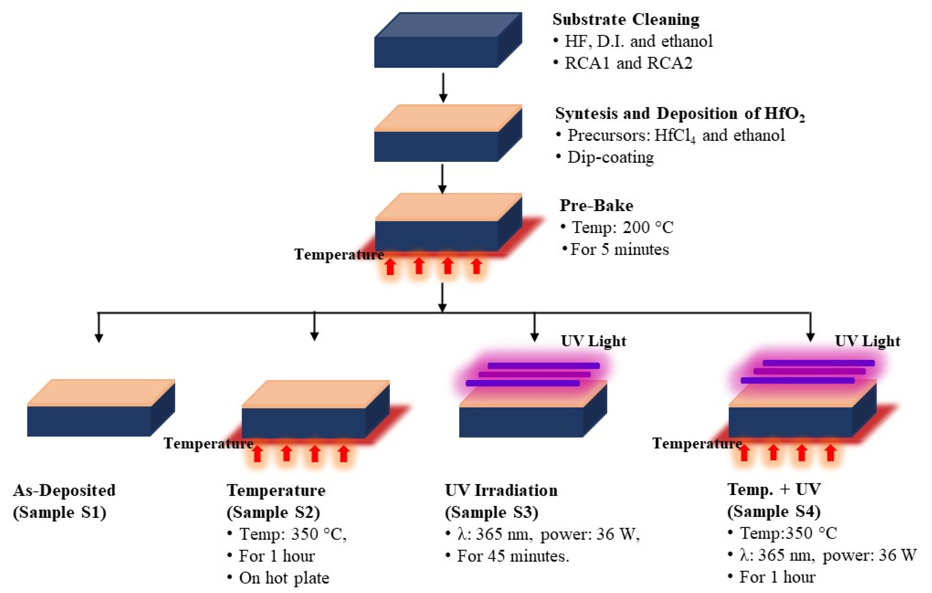
2. Materials and Methods

HfO2 thin films were deposited on (100) p-type silicon substrates (p-Si) by the dip-coating technique. First, substrates were cleaned by the HF solution, deionized (DI), water, and ethanol, and then by the RCA1 (5 DI H2O: 1 NH4OH: 1H2O2 at 70 °C) and RCA2 (6 DI H2O: 1 HCl: 1 H2O2 at 70 °C) processes. All reactants are electronic grade and were purchased from Sigma-Aldrich (St. Louis, MA, USA). Thereafter, 5.16 g of hafnium chloride (HfCl4, 99.99% Sigma-Aldrich, St. Louis, MA, USA) was dissolved into 40 mL of ethanol. Four samples were prepared by dipping the substrates into the prepared solution at room temperature for 20 s using a 10 cm/min immersion speed. After being removed from the bath, all the samples were baked in the air for 5 min at 200 °C (sample S1). Afterwards, another sample was air-annealed at 350 °C by 1 h (sample S2). Another sample was irradiated with a UV LED source centered at 380 nm and 36 W for 1 h (sample S3), with a sample–lamp separation of 5 cm. The later sample (sample 4) was simultaneously air-annealed at 350 °C during UV irradiation for 1 h. Figure 1 shows a flow diagram of the process and the samples prepared.
Films were characterized by grazing incidence X-ray diffraction (GIXRD) in a Siemens D5000 instrument (Siemens, Munich, Germany), using Cu Kα radiation (0.15408 nm), at an incidence angle of 1°, a step size of 0.02°, and a step time of 3 s. Raman spectroscopy was performed in a Raman i-Plus spectrometer (BW Tek, Plainsboro, NJ, USA), with a 532 nm laser with a nominal power of 36 mW, focused through a 20× microscope objective. UV–visible spectroscopy in the diffuse reflectance mode was performed in a Varian Cary 5000 Instrument (Varian Inc., Palo Alto, CA, USA) using an integrating sphere. Optical fluorescence spectroscopy was performed using an excitation wavelength of 270 nm in a Horiba-Jobin Yvon instrument. Atomic force microscopy was conducted in a TT AFM Workshop instrument (Hilton Head Island, SC, USA) in the intermittent contact mode, using a DLC-coated tip with a 190 µm cantilever with a resonance frequency of 190 kHz and a constant force of 48 N/m. To obtain the film’s resistivity, 4-point measurements were carried out in a Signatone Pro SP 4 instrument (Signatione, Sunnyvale, CA, USA) with a tip separation of 0.1 cm, and a bias was applied from −5 to + 5 V.

3. Results

White, adherent films, with a thickness of 0.95 ± 0.15 µm, calculated from reflectance spectra [11], were obtained. With the aim of determining the effect of the post-deposition treatments on the structural, optical, morphological, electric, and electronic characterization of the HfO2 films, this section presents the GIXRD, Raman, AFM, electrical, fluorescence, and UV-Vis reflectance data.

3.1. Structural Characterization

3.1.1. X-ray Diffraction

Figure 2 presents the grazing incidence X-ray diffractograms of the p-Si substrate and the S1–S4 samples, compared with the powder diffraction file PDF 36-0104 corresponding to the monoclinic phase of HfO2. The S1 and S2 films present diffraction peaks at 2 theta 29.24° as well as 2 theta 29.24° and 32.62°, respectively, related with the (−111) and (111) reflections of monoclinic HfO2 [4,5]. The presence of the second peak of the (111) plane in sample S2, annealed at 350 °C, indicates higher crystallinity. The observed 2 theta shift of 1° of both peaks with respect to the reported PDF is related to the low X-ray incidence angle. S3 and S4 films did not present diffraction peaks apart from the Si substrate, indicating that the UV process led to amorphous films. Future work will explore the effect of film crystallinity when varying both the temperature and annealing time around the monoclinic phase dominion [4,5] and its effect on the film’s electronic properties.

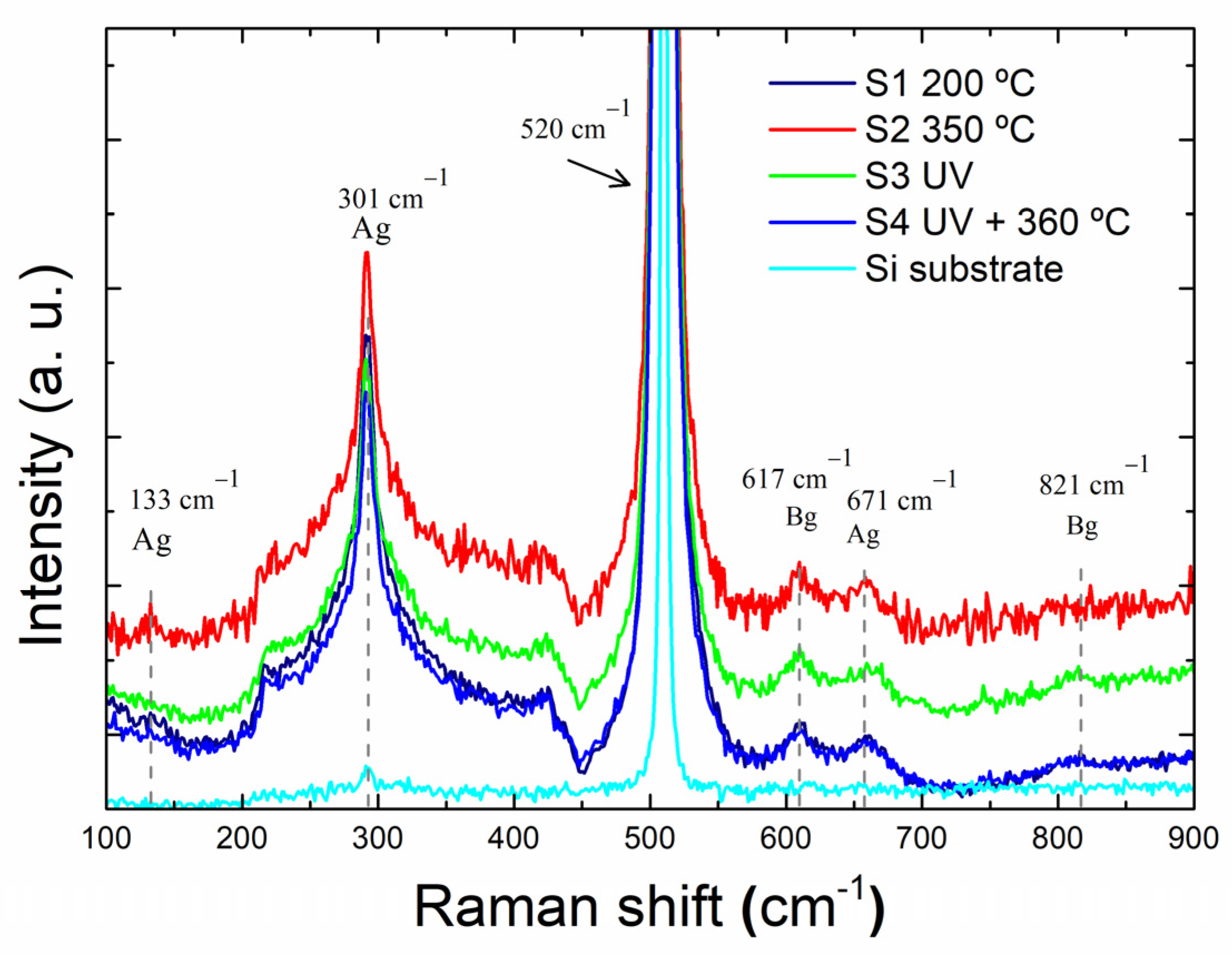
3.1.2. Raman Spectroscopy

Figure 3 shows the Raman spectra of the four HfO2 samples and p-Si as the reference sample (P1). The monoclinic HfO2 structure has 18 optical phonon modes, which are (9Ag + 9Bg) for Raman active modes and (8Au + 8Bu) for IR-active [8]. Figure 3 depicts optical vibration modes centered at 133 cm−1 (Ag mode), 301 cm−1 (Ag mode), 617 cm−1 (Bg mode), 671 cm−1 (Ag mode), and 821 cm−1 (Bg mode).
The most intense peak corresponds to the 301 cm−1 vibration related to Hf-Hf bonds and the formation of oxygen vacancies [5,9]. A defined peak at 133 cm−1 arises in the spectrum of the S2 sample in accordance with the higher crystallinity of the sample. Nevertheless, there are only slight differences in the peak intensities between the films; therefore, not much information can be derived from the effect of the post-deposition treatment on the local film structure.

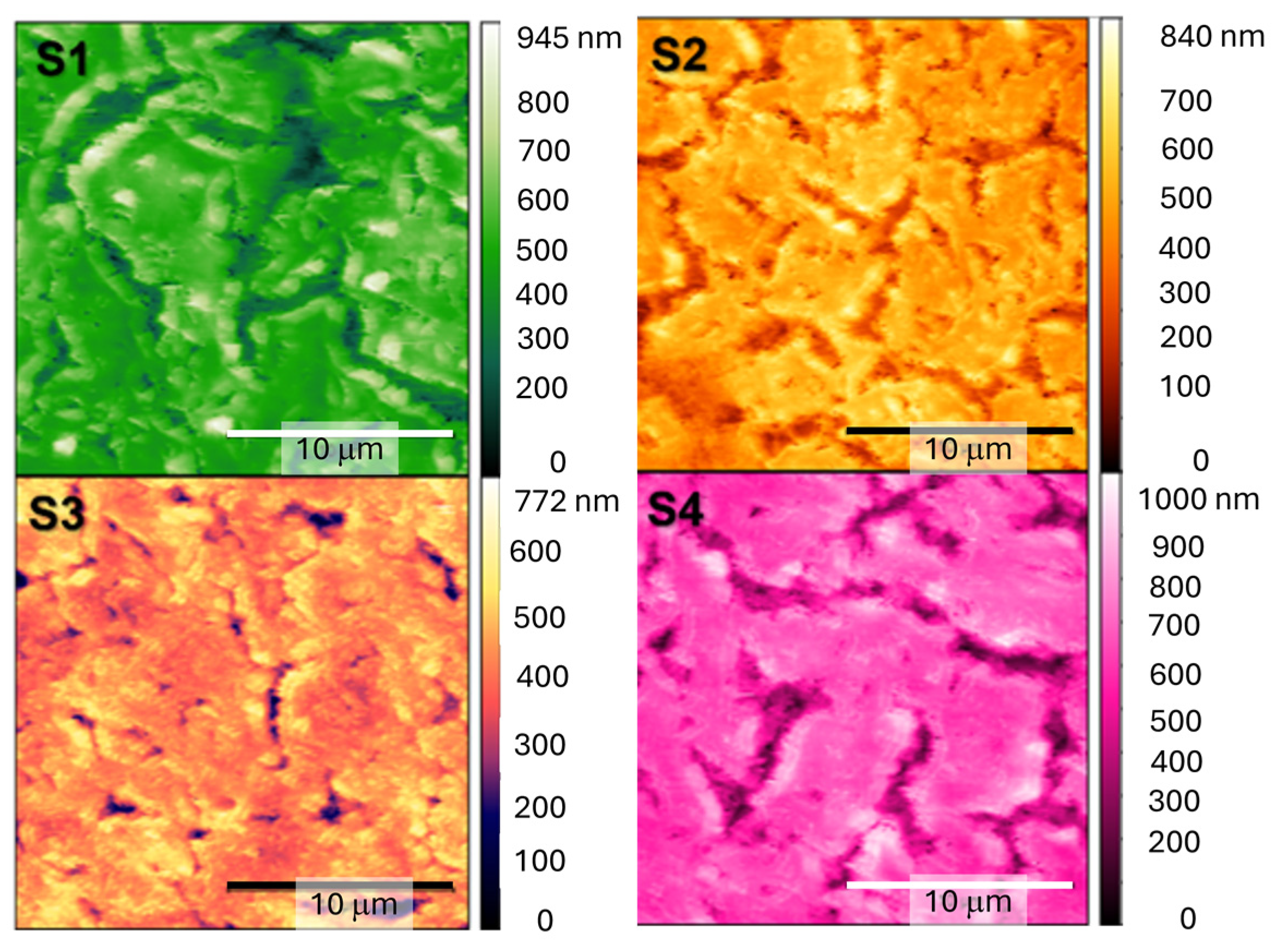
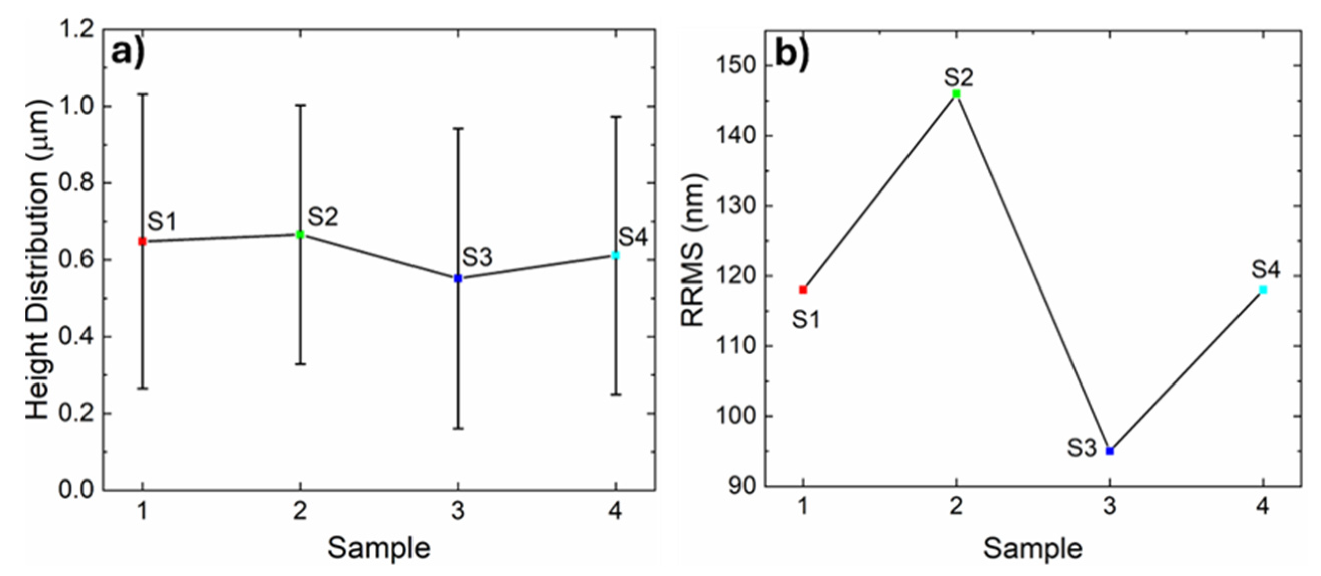
3.2. Film Morphology by Atomic Force Microscopy

Figure 4 presents the 20 × 20 µm2 topographic images of the S1–S4 HfO2 thin films. Initially, the image of the S1 film shows a cracked surface with some spherical particles spread on the surface. The characteristic cracked morphology of the HfO2 films may be due to the type of deposition used, the dip coating, and the results of solvent evaporation on the observed morphology, opposite to the film morphology achieved by sputtering [12]. Upon thermal annealing at 350 °C, the size of the cracks decreased in the S2 film, indicating that the films became more compact. When UV radiation was applied to the S3 film, a decrease in the width and the length of the cracks was observed, indicating coalescence of the films, explained by the sequential bond rupture and decomposition of remnants of organic groups [7,13] by UV radiation, followed by the “plastic” self-healing of the film which led to the amorphization observed in the GIXRD [14]. However, in the S4 film, where both treatments (thermal and UV radiation) were combined, a further increase in the depth and size of the cracks occurred, suggesting that the bond rupture was not followed by recrystallization. Vargas et al. [4] and Zhang et al. [13] showed that increasing annealing temperature in HfO2 films led to increased film compacity, which has been attributed to the decomposition of organic groups either in dip-coated or ALD films; on the other hand, Kumar et al. observed more compact and smooth surfaces upon UV/O3 treatment [7], in correspondence with the present results. A study of increased annealing time at low temperatures coupled with UV irradiation to increase coalescence should be explored in future work.
In Figure 5, (a) height distribution and (b) roughness root mean square values obtained from the AFM images are presented.
As derived from topographic images (Figure 4), in Figure 5a, the height distribution is almost constant in S1 and S2 with 0.64 and 0.66 µm, respectively, with the value of heights decreasing in S3 to 0.54 µm and the value increasing in S4 to 0.61 µm, obtaining a value closer to S1. In Figure 5b, the RRMS shows a similar behavior; the RRMS has a value of 118 nm of roughness in S1, increasing in S2 to 146 nm, followed by a decrease in S3 to 95 nm and an increase again in S4 to 118 nm, returning to the value obtained in S1.
S1 and S4 present similar values in the distribution of heights and roughness, although S4 applied heat treatment and UV irradiation and, according to the literature, there should be an increase in the crystallinity of the HfO2 film [12], which would contribute to an improvement in its morphological properties; however, S4 shows values and properties similar to those presented in S1, which could be due to the extended time of heat treatment and irradiation, generating a rupture of bonds in the structure of the film. The results are correspondent with those in the X-ray diffraction analysis, where it was found that S3 and S4 are amorphous.
In future work, optimal heat treatment and UV irradiation times will be assessed to tailor the film compacity/porosity, which could benefit their use as insulators in TFTs or in electrocatalytic applications, respectively.

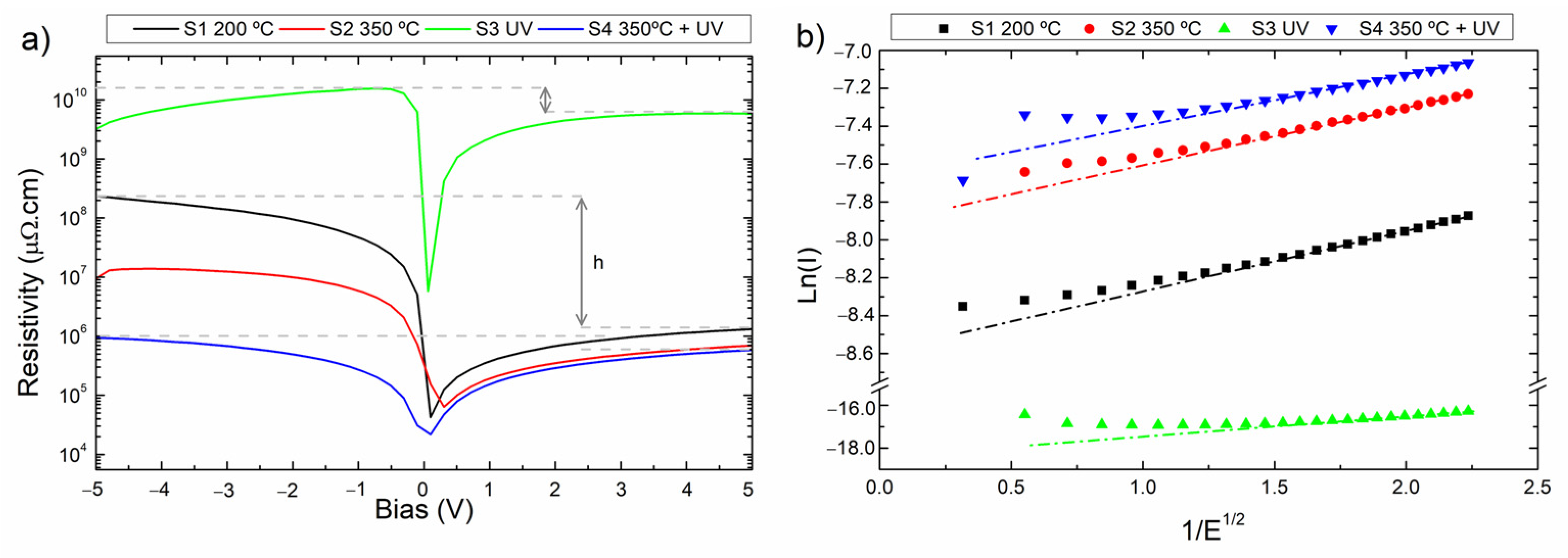
3.3. Electrical Characterization

Figure 6 presents the electrical characterization of the films. The film resistivity was calculated from the four-point measurement both in forward and reverse bias at ±5 V, as shown in Figure 6a. The film resistivities in forward bias range from 6 × 10⁵–1.4 × 10⁶ Ω.cm in the S1, S2, and S4 samples, while sample S3 has a maximum forward resistivity of 6 × 10⁹ Ω.cm. On the other hand, sample S1, treated at 200 °C, has the highest resistivity difference (h in Figure 6a) between the maxima at forward and reverse bias, while this difference reduces upon post-deposition treatment, as illustrated by the grey arrows in Figure 6a. The lowest resistivity and lowest h-difference occurred in the S4 sample, treated with UV irradiation and annealed at 350 °C, which suggests a nearly conductive film due to the high concentration of oxygen vacancies [15]. In contrast, the sample with the highest resistivity, S3, which was only irradiated with UV, may have more electronic traps that would avoid forward conduction and, correspondingly, reduce the barrier in reverse bias, as shown in Figure 6a. Figure 6b presents the Schottky plots for ln (I) vs. 1/E2 of the films. Samples S1 and S2 have good linear behavior, indicating that these are the predominant conduction mechanisms, while samples S3 and S4 have a negative slope region at low 1/E2 values followed by a linear region, indicating more than one conduction mechanism, which can be explained by the formation of defects during UV irradiation [16].

3.4. Optoelectronic Properties

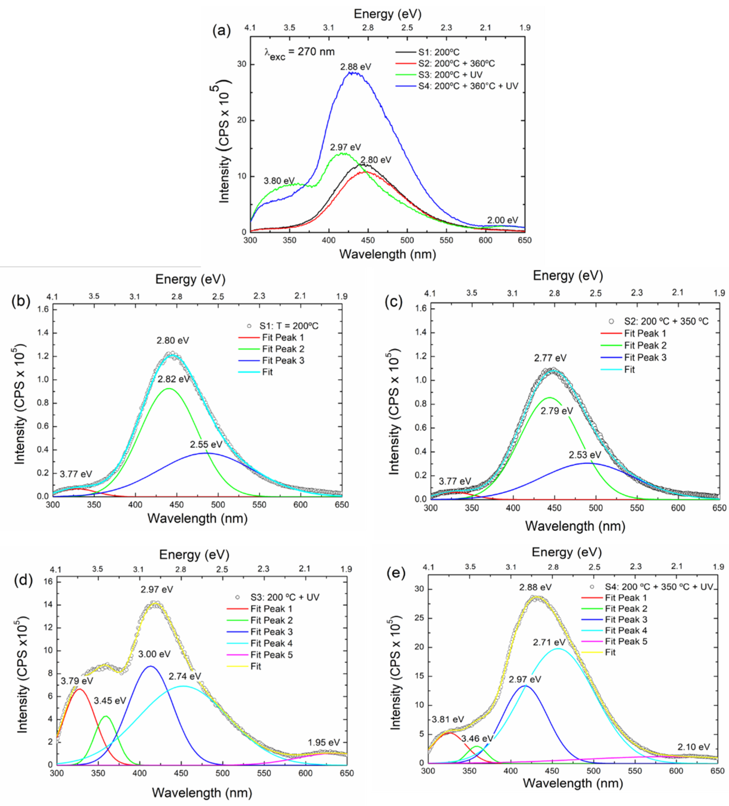
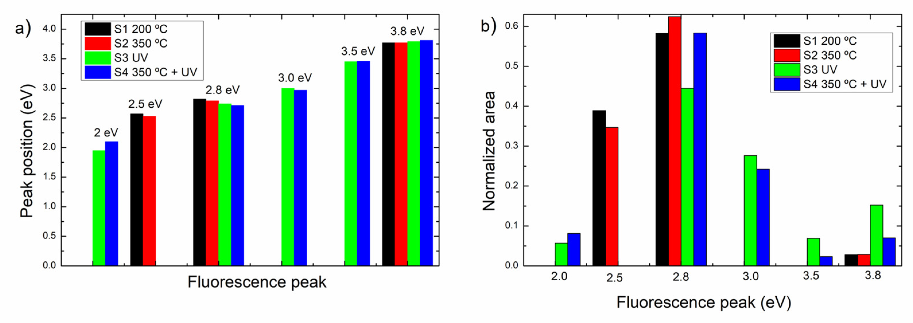
3.4.1. Optical Fluorescence

Figure 7a presents the fluorescence spectra of samples S1–S4 performed with an excitation wavelength of 270 nm. It can be observed that S1 and S2 samples present the lowest total fluorescence while S4 presents the highest, suggesting that this film has the highest defect density [17]. Emission maxima are evident at ca. 2.0 eV, 2.8 eV, 2.9 eV, 3.0 eV, and 3.8 eV. S1 and S2 spectra display fewer fluorescence features than S3 and S4. Figure 7b–e show the deconvoluted emission spectra of the samples.
As shown in Figure 7a, the intensity and position of the fluorescence bands differ upon the film treatment. For semiquantitative characterization, Figure 8 presents the analysis of the fluorescence peaks, where Figure 7a shows the peaks observed in each spectrum after deconvolution and the corresponding peak positions, and Figure 7b displays the areas of the peaks, normalized with the total area under the fluorescence emission curve, as a measure of the relative density of the electronic states contributing to the emission.
As observed in Figure 8a, samples S1 (treated at 200 °C) and S2 (treated at 200 °C and then at 350 °C) display three emission peaks at ca. 2.5 eV, 2.8 eV, and 3.8 eV. Correspondingly, samples S3 and S4, which have UV treatment, display additional emission peaks at ca. 2 eV, 3 eV, and 3.5 eV. The peak at 2.8 eV presents an evident red shift from 2.82 eV (S1) to 2.71 eV (S4), while the position of the emission at 3.8 eV is almost invariant. These bands are congruent with those reported in [18].
The emission band at 2.5 eV has been related either to hydrogen or chlorine defects [19], and it is only present before UV treatment. The emission band at 2.8 eV is characteristic of oxygen vacancy defects in HfO2 [10]. On the other hand, the bands at 2.0, 3.0, and 3.5 eV, which appear only after treatment with UV light, may arise from dangling bonds and defect centers [1]. The increase in emissions due to the defects in S3 and S4 films corresponds with the XRD analysis, where it was found that S3 and S4 are amorphous. The band at 3.8 eV may arise from direct recombination from shallow states within the gap to the valence band [20] but has also been attributed to the OH radical within the structure [17].
With respect to the relative contribution of each band to the fluorescence spectrum, Figure 8b presents the normalized areas of the fluorescence peaks. It can be observed that the dominant emissions in all the samples arise from the oxygen vacancies at 2.8 eV, although its relative intensity is variable with the sample treatment and the presence of additional emission bands upon UV treatment. For example, in S3, the 2.8 eV emission is lower than that in S4, but the emissions at 3.0, 3.5, and 3.8 eV are higher in S3 than in S4, indicating a reduction in the available states with the UV + annealing at 350 °C. The band at ca. 2.5 eV, related to hydrogen/chlorine defects, reduced its relative intensity with the increase in temperature from S1 to S2.
The results indicate that the electronic structure of HfO2 films is largely influenced by the UV treatment, which causes an increase in the defect states, which are partially reduced with the annealing temperature. More accurate defect engineering would be possible with optimized annealing temperature and time and UV irradiation times.

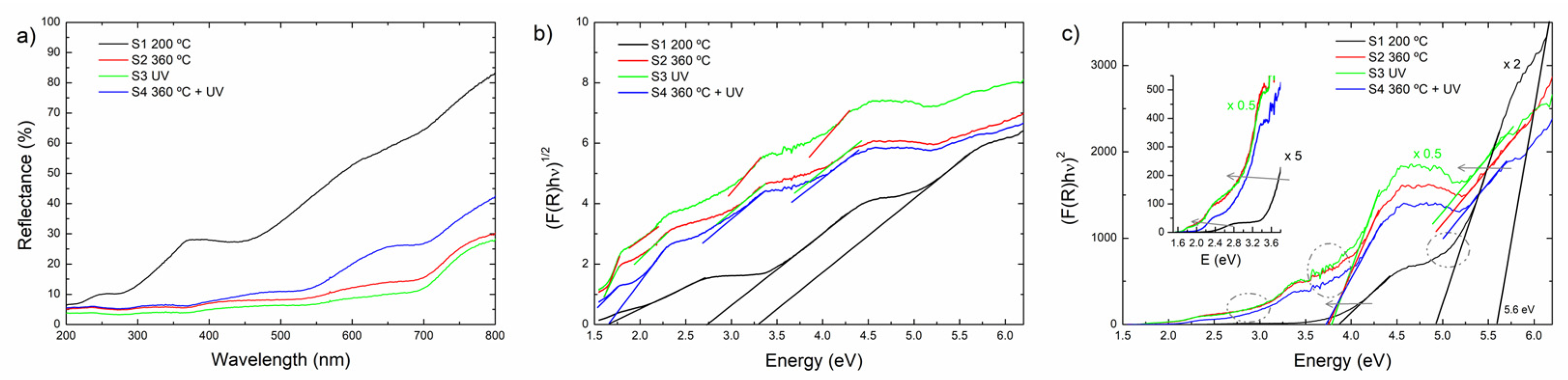
3.4.2. UV–Visible Spectroscopy
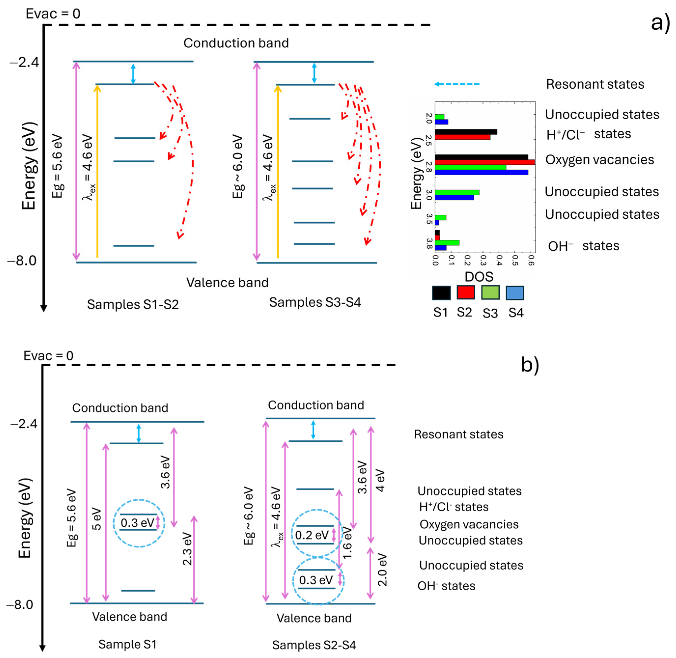
S1–S4 samples were analyzed by UV–Vis diffuse reflectance spectroscopy for a wavelength range of 200 to 800 nm. By applying the Kubelka–Munk function (FK-M), the optical absorption coefficient, α, was estimated using the following equation:
α ~ F ( K M ) = 1 R 2 2 R
where R is diffuse reflectance.
To assess the electronic states near the absorption edge, the following expression as a function of FK-M was used:
h ν α ~ h ν F ( K M ) A h ν E g n
where A is a constant that does not depend on the photon energy, h is plank constant, ν is the frequency, Eg is the band gap, and n can take the values 0.5 or 2 depending on if the band gap is direct or indirect [21]. The band gap for HfO2 has been reported as indirect at ca. 6 eV [4] and direct at ca. 5.8 eV [11]. Figure 9 shows the analysis of the optical reflectance of the S1–S4 samples. Figure 9a shows the reflectance spectra, Figure 9b shows the Tauc plot (F(R)hν)0.5 vs. , which corresponds to indirect transitions, and Figure 9c shows the Tauc plots (F(R)hν)2 vs. corresponding to the direct transitions for the S1–S4 HfO2 samples, respectively [21]. These results, which show both direct allowed and indirect allowed transitions in HfO2 films, are consistent with those reported by Shilov et al. [22] for HfO2 powders, but this has not been reported in HfO2 films, as far as revised in the literature.
The reflectivity of the films decreases from higher to lower wavelengths according to the reported refractive index vs. wavelength [4]. From Figure 9a, it can be observed that film S1 has the highest reflectivity vs. wavelength behavior (%R from 5 to 80%). It has been reported that the refractive index increases with the temperature [4]. The other reflectance spectra have similar reflectivity values and features, also suggesting an increased density upon post-deposition treatments [4]. Figure 9b shows the optical behavior of the films when indirect transitions (F(R)hv1/2 vs. energy plot) are assessed. In the plot, several linear regions are indicated with straight lines for each spectrum, indicating the presence of delocalized states within the band gap. It is evident that there is a difference in such states from the S1 sample to the samples with post-deposition treatment. In Figure 9c, the F(R)hv2 vs. energy plot, which accounts for direct transitions, is shown. Several linear regions are indicated at around 5, 3.5–4.0, 2.6–3.0, and 2 eV. The gray arrows indicate the trend of the transition values. The spectrum of the S1 sample shows a defined transition at ca. 5.6 eV, which can be assigned to the direct band gap of HfO2 [11], followed by another defined state at ca. 5 eV, the nature of which is discussed below. Correspondingly, the spectra of samples S2–S4 have similar features, but the fundamental transition is not observed, possibly due to the spectral range where the transmittance was assessed [4]. The areas within dashed circles indicate extended absorption tails around 5.0 eV, 3.8 eV, and 2.8 eV, respectively, related to the disorder and widening of the density of available states around these energies within the mobility gap.
Following Ibrahim and Al-Ani [21], the intersections where y = 0 in the plot are not necessarily an electronic transition but depend on the disorder degree and can be considered extrapolations from delocalized states to the zero of density states, according to the Davis–Mott model. Thus, in Figure 10, the energy values of the extrapolations at y = 0 of the indirect- and direct-related transitions are shown. In Figure 10a, corresponding to F(R)hv1/2 = 0, sample S1 presents y = 0 at 1.45 eV, 1.65 eV, 2.75 eV, and 3.2 eV, while samples S2–S4 display states at 1.25 eV, 1.45 eV, 1.65 eV, and 2.0 eV. Correspondingly, the F(R)hv2 = 0 plots have several states; sample S1 has y = 0 at 2.3 eV, 3.6 eV, 5.0 eV, and the fundamental band gap at 5.6 eV, and samples S2–S4 have states at 1.65 eV, 2.0 eV, 2.8 eV, 3.6 eV, and 4 eV, as observed in Figure 10b.

4. Discussion

Figure 11 summarizes the results from fluorescence and UV–visible spectroscopy with two electronic band diagrams. Figure 11a presents the electronic band diagrams from the fluorescence data for samples S1–S2 (left) and samples S3–S4 (right). The positions of the conduction band and valence band edges were calculated from González et al.’s data [8]. The dashed, red arrows indicate the radiative transitions. The level below the conduction band corresponds to empty levels where electrons arrive at 270 nm excitation to then produce radiative decay. This level has been observed by several authors [18,23,24,25,26] and it has been attributed either to defect states related to the observed Urbach tail below the band gap in polycrystalline HfO2 [20] or to resonant states originating from the presence of localized Hf 5 d polaron states at the Fermi level, which, in turn, push the unoccupied states at 2 eV above the Fermi level [22,23]. These polaron states arise from the oxygen vacancies indicated by the fluorescence band at 2.8 eV [18,21,22,23]. The levels within the mobility gap were assigned considering the observed fluorescence bands. As described in Section 3.4.1, in S1 and S2 samples, the observed fluorescence peaks are associated with H+/Cl states [17], oxygen vacancies, and OH-states [16], respectively. The thermal treatment at 350 °C increases the number of oxygen vacancies, while upon UV treatment, the peak associated with oxygen vacancies at 2.8 eV is reduced, but novel transitions at 2 eV, 3 eV, and 3.5 eV are observed. Also, the H+ states are not observed in samples S2 and S4, and there is an increase in the fluorescence intensity of OH states, in contradiction with the results from Kim et al. [14], who reported that UV + rapid thermal annealing at 450 °C led to a reduction in OH states, which confirms the possibility of tailoring the defect states with a careful selection of UV and thermal treatment conditions. From this diagram, it is possible to state that the normalized areas of the fluorescence peaks are, then, a measure of the density of the electronic states within the mobility gap, as shown on the right side of Figure 11a.
Figure 11b shows the electronic band diagram for the S1 (left) and S2–S4 samples (right) from the point of view of direct electronic transitions within the mobility gap calculated from the F(R)hv2 = 0 plot [21]. In this diagram, the depicted transitions were assigned considering the fluorescence bands and the discussed assignation to different electronic states. For the case of sample S1, the direct band gap was directly obtained from the F(R)hv2 = 0 plot as well as the transition at 5 eV, which was already assigned to the resonant states below the band gap [22,23]. The transitions at 3.6 eV and 2.3 eV arose from the occupied oxygen vacancy levels to the conduction band and from the valence band to unoccupied H+ states, respectively. The oxygen vacancy levels and H+ levels were very close (ca. 0.3 eV), which may lead to thermalization, thus explaining the high DOS for the H+ level. For samples S2–S4, the fundamental VB-CB transition was not observed due to an increase in Eg in these samples, but as the samples presented fluorescence upon excitation at 270 nm, the resonant states were kept in the diagram, and Eg was set at 6 eV. Thus, the transition from the oxygen vacancy level to the CB was still observed at 3.6 eV, and a new 4 eV transition arose from the novel states, which may be a result of the varying levels of Hf 5d and O 2p both up and down [23]. This new state is 2 eV above the valence band maximum, which is of interest for photocatalytic applications [8]. The blue dotted circles in Figure 11b indicate the presence of extended absorption tails, which explain the variations in the transition values, as observed in Figure 10. With respect to the indirect transitions, many of them showed a sharp onset, which is consistent with the Davies–Mott model for amorphous semiconductors [19]. The electrical behavior of samples can now be discussed in light of the proposed electronic diagrams. In the case of S1 sample, conduction occurred predominantly through the oxygen vacancies [27]. After thermal annealing at 350 °C, resistivity was lowered by the increase in oxygen vacancies, as depicted in Figure 11a. In the case of samples S3 and S4, which were UV-irradiated, novel unoccupied states at 3.5 eV and 3.8 eV were formed, which decreased the difference h described in Section 3.3, acting as traps for electrons injected into the conduction band [27]. On the other hand, the oxygen vacancy states increased in S4 with respect to S3, while the trap states at 3.5 eV and 3.8 eV were reduced, and the state close to the valence band around 2 eV increased, which, on the whole, may explain the metallic-like behavior of the S4 sample and the large resistivity and rupture for the reverse bias of sample S3. Thus, the electrical properties of HfO2 could be controlled by the balance between the intrinsic oxygen vacancies and the states tailored by post-deposition treatments.
As a final consideration, the results suggest that in addition to doping [8] or preparing heterostructures [9,10], it is possible to tailor the electronic structure of HfO2 using an adequate selection of thermal and UV treatment for photocatalytic/electrocatalytic applications. Also, the present study sheds more light on the defects that control the performance of HfO2 for its potential applications in microelectronics, electro and photocatalysis, and optical devices.

5. Conclusions

In the present work, HfO2 films prepared by room-temperature dip coating were treated at different conditions after deposition onto p-Si. Films were characterized by XRD, Raman, AFM, UV-Vis, and fluorescence spectroscopy. The films were monoclinic after thermal treatment at 350 °C and became amorphous and more compact upon UV treatment. A band diagram that considered both optical and fluorescence spectroscopy was proposed, including normalized fluorescence as a measure of the Density of States. The results indicate that UV treatment generates several defect states within the mobility gap, which may decrease the performance of HfO2 films in microelectronics but may also allow their use in optoelectronic, photocatalytic, and electrocatalytic applications.

Author Contributions

Conceptualization, F.L.-H. and F.C.-B.; methodology, S.S.-R. and F.I.G.-M.; validation, R.M.W.-G., A.L.H.-M. and F.L.-H.; formal analysis, F.C.-B.; investigation, S.S.-R. and F.I.G.-M.; resources, A.L.H.-M.; data curation, R.M.W.-G. and A.L.H.-M.; writing—original draft preparation, S.S.-R., F.I.G.-M., R.M.W.-G., F.L.-H. and F.C.-B. writing—review and editing, F.I.G.-M. and F.C.-B.; visualization, F.I.G.-M. and F.C.-B.; supervision, R.M.W.-G., A.L.H.-M. and F.L.-H.; project administration, F.L.-H.; funding acquisition, F.L.-H. All authors have read and agreed to the published version of the manuscript.

Funding

This research was funded by CONAHCYT, grant numbers 2019-40798 and 2022-321595. GIXRD analyses was carried out at the National Laboratory of Nano and Biomaterials (LANNBIO), CINVESTAV-IPN, which is financed by the FOMIX-Yucatán grant numbers 2008-108160, CONACYT LAB-2009-01-123913, 292692, 294643, 188345 and 204822.

Institutional Review Board Statement

Not applicable.

Informed Consent Statement

Not applicable.

Data Availability Statement

The original contributions presented in this study are included in the article. Further inquiries can be directed to the corresponding author.

Acknowledgments

We thank Patricia Quintana for the access to LANNBIO, to Daniel Aguilar for obtaining the diffractograms, and to Mario Herrera, Ariel Bagundo and Daniel Brito for instrument maintenance. The access to four-point tests was enabled by Edna De la Cruz-Terrazas.

Conflicts of Interest

The authors declare no conflicts of interest. The funders had no role in the design of the study; in the collection, analyses, or interpretation of data; in the writing of the manuscript; or in the decision to publish the results.

References

  1. Hong, S.; Park, S.P.; Kim, Y.-G.; Kang, B.H.; Na, J.W. Low-temperature fabrication of an HfO2 passivation layer for amorphous indium–gallium–zinc oxide thin film transistors using a solution process. Sci. Rep. 2017, 7, 16265. [Google Scholar] [CrossRef] [PubMed]
  2. Yoo, Y.B.; Park, J.H.; Lee, K.H.; Lee, H.W.; Song, K.M.; Leec, S.J.; Baik, H.K. Solution-processed high-k HfO2 gate dielectric processed under softening temperature of polymer substrates. J. Mater. Chem. C 2013, 1, 1651–1658. [Google Scholar] [CrossRef]
  3. Kim, W.; Bang, J.-H.; Uhm, H.-S.; Lee, S.-H.; Park, J.-S. Effects of post plasma treatment on material properties and device characteristics in indium zinc oxide thin film transistors. Thin Solid Film. 2010, 519, 1573–1577. [Google Scholar] [CrossRef]
  4. Vargas, M.; Murphy, N.R.; Ramana, C.V. Structure and optical properties of nanocrystalline hafnium oxide thin films. Opt. Mater. 2014, 37, 621–628. [Google Scholar] [CrossRef]
  5. Tan, T.; Liu, Z.; Lu, H.; Liu, W.; Tian, H. Structure and optical properties of HfO2 thin films on silicon after rapid thermal annealing. Opt. Mater. 2010, 32, 432–435. [Google Scholar] [CrossRef]
  6. Rauwel, E.; Galeckas, A.; Rauwel, P. Photoluminescent cubic and monoclinic HfO2 nanoparticles: Effects of temperature and ambient. Mater. Res. Express 2014, 1, 015035. [Google Scholar] [CrossRef]
  7. Kumar, M.; Jeong, H.; Lee, D. Effect of UV/ozone plasma treatment on sol–gel-derived HfO2 thin films. Ceram. Int. 2017, 43, 1174–1179. [Google Scholar] [CrossRef]
  8. González, L.A.; Gálvez-Barboza, S.; Vento-Lujano, E.; Rodríguez-Galicia, J.L.; García-Cerda, L.A. Mn-modified HfO2 nanoparticles with enhanced photocatalytic activity. Ceram. Int. 2020, 46, 13466–13473. [Google Scholar] [CrossRef]
  9. Jayaraman, V.; Mahalingam, S.; Chinnathambi, S.; Pandian, G.N.; Prakasarao, A.; Ganesan, S.; Ramasamy, J.; Ayyaru, S.; Ahn, Y.-H. Facile Synthesis of Hafnium Oxide Nanoparticle Decorated on Graphene Nanosheet and Its Photocatalytic Degradation of Organic Pollutants under UV-Light Irradiation. Appl. Sci. 2022, 12, 11222. [Google Scholar] [CrossRef]
  10. Jeffery, A.A.; Chougule, S.S.; Hasan, I.; Alagarasan, J.K.; Sankar, P.R.; Somu, P.; Lin, M.-C.; Kumarasamy, K.; Ahn, Y.-H.; Murugasamy, J. Oxygen-Vacancy-Rich HfO2–x Nanoparticles Supported on Reduced Graphene Oxide for Electrocatalytic Hydrogen Evolution Reactions. ACS Appl. Nano Mater. 2023, 6, 23053–23063. [Google Scholar] [CrossRef]
  11. Condurache-Bota, S.; Tigau, N.; Drasovean, R. Explicit application of Swanepoel’s method for the analysis of Sb2O3 films. J. Sci. Arts 2010, 2, 335–340. [Google Scholar]
  12. Araiza, J.d.J.; Álvarez-Fraga, L.; Gago, R.; Sánchez, O. Surface morphology and optical properties of hafnium oxide thin films produced by magnetron sputtering. Materials 2023, 16, 5331. [Google Scholar] [CrossRef] [PubMed]
  13. Zhang, F.; Liu, G.; Liu, A.; Shin, B.; Shan, F. Solution-processed hafnium oxide dielectric thin films for thin-film transistors applications. Ceram. Int. 2015, 41, 13218–13223. [Google Scholar] [CrossRef]
  14. Kim, J.; Park, J.; Pham, D.P.; Yeo, M.S.; Rhee, H.; Kim, Y.-S.; Cho, E.-C.; Yi, J. Combination of ultraviolet exposure and thermal post-treatment to obtain high quality HfO2 thin films. Ceram. Int. 2021, 47, 9643–9650. [Google Scholar] [CrossRef]
  15. Jancovic, P.; Hudec, B.; Dobrocka, E.; Dérer, J.; Fedor, J.; Fröhlich, K. Resistive switching in HfO2-based atomic layer deposition grown metal–insulator–metal structures. Appl. Surf. Sci. 2014, 312, 112–116. [Google Scholar] [CrossRef]
  16. Yuan, F.-Y.; Deng, N.; Shih, C.-C.; Tseng, Y.-T.; Chang, T.-C.; Chang, K.-C.; Wang, M.-H.; Chen, W.-C.; Zheng, H.-X.; Wu, H.; et al. Conduction Mechanism and Improved Endurance in HfO2-Based RRAM with Nitridation Treatment. Nanoscale Res. Lett. 2017, 12, 574. [Google Scholar] [CrossRef]
  17. Mercado, C.; Seeley, Z.; Bandyopadhyay, A.; Bose, S.; McHale, J.L. Photoluminescence of Dense Nanocrystalline Titanium Dioxide Thin Films: Effect of Doping and Thickness and Relation to Gas Sensing. ACS Appl. Mater. Interfaces 2011, 3, 2281–2288. [Google Scholar] [CrossRef]
  18. Kong, M.; Li, B.; Guo, C.; Zeng, P.; Wei, M.; He, W. The Optical Absorption and Photoluminescence Characteristics of Evaporated and IAD HfO2 Thin Films. Coatings 2019, 9, 307. [Google Scholar] [CrossRef]
  19. Aarik, J.; Mandar, H.; Kirm, M.; Pung, L. Optical characterization of HfO2 thin films grown by atomic layer deposition. Thin Solid Film. 2004, 466, 41–47. [Google Scholar] [CrossRef]
  20. Papernov, S.; Brunsman, M.D.; Oliver, J.B.; Hoffman, B.N.; Kozlov, A.A.; Demos, S.G.; Shvydky, A.; Cavalcante, F.H.M.; Yang, L.; Demoni, C.S.; et al. Optical properties of oxygen vacancies in HfO2 thin films studied by absorption and luminescence spectroscopy. Opt. Express 2018, 26, 17608–17623. [Google Scholar] [CrossRef]
  21. Ibrahim, A.; Al-Ani, S.K.J. Models of optical absorption in amorphous semiconductors at the absorption edge -a revie w and re-evaluation. Czechoslov. J. Phys. 1994, 44, 785–797. [Google Scholar] [CrossRef]
  22. Shilov, A.O.; Savchenko, S.S.; Vokhmintsev, A.S.; Gritsenko, V.A.; Weinstein, I.A. Thermal quenching of self-trapped exciton luminescence in nanostructured hafnia. J. Lumin. 2022, 247, 118908. [Google Scholar] [CrossRef]
  23. Nguyen, N.V.; Davydov, A.V.; Chandler-Horowitz, D.; Frank, M.M. Sub-bandgap defect states in polycrystalline hafnium oxide and their suppression by admixture of silicon. Appl. Phys. Lett. 2005, 87, 192903. [Google Scholar] [CrossRef]
  24. Cisneros-Morales, M.C.; Aita, C.R. The effect of nanocrystallite size in monoclinic HfO2 films on lattice expansion and near-edge optical absorption. Appl. Phys. Lett. 2010, 96, 191904. [Google Scholar] [CrossRef]
  25. Perevalov, T.V.; Aliev, V.S.; Gritsenko, V.A.; Saraev, A.A.; Kaichev, V.V.; Ivanova, E.V.; Zamoryanskaya, M.V. The origin of 2.7 eV luminescence and 5.2 eV excitation band in hafnium oxide. Appl. Phys. Lett. 2014, 104, 071904. [Google Scholar] [CrossRef]
  26. Wang, Z.; Yu, H.; Su, H. The transport properties of oxygen vacancy-related polaron-like bound state in HfOx. Sci. Rep. 2013, 3, 3246. [Google Scholar] [CrossRef]
  27. Wu, J. Impact of oxygen vacancies on monoclinic hafnium oxide and band alignment with semiconductors. Mater. Today Commun. 2020, 25, 101482. [Google Scholar] [CrossRef]
Figure 1. Process flow diagram used for the production of HfO2 samples.
Applsci 15 01573 g001
Figure 2. Grazing incidence X-ray diffractograms of the p-Si substrate and the S1–S4 HfO2 samples compared with the monoclinic powder diffraction file, PDF 36-0104.
Applsci 15 01573 g002
Figure 3. Raman spectra of HfO2 samples S1–S4 and p-Si substrate. Raman spectra were acquired with a 532 nm laser.
Applsci 15 01573 g003
Figure 4. The 20 × 20 µm2 AFM topographic images of the S1–S4 HfO2 thin films.
Applsci 15 01573 g004
Figure 5. (a) Height distribution graph and (b) roughness root mean square (RRMS) of HfO2 thin films.
Applsci 15 01573 g005
Figure 6. Resistivity vs. bias voltage (a) and Schottky plots (b) of the HfO2 samples. The lines in (b) are guides for the eye.
Applsci 15 01573 g006
Figure 7. Fluorescence spectra of (a) all the samples; (be) deconvoluted fluorescence spectra of (b) S1, (c) S2, (d) S3, and (e) S4.
Applsci 15 01573 g007
Figure 8. (a) The position of the fluorescence peaks and (b) normalized intensity with respect to the total fluorescence area of the fluorescence peaks of samples S1–S4.
Applsci 15 01573 g008
Figure 9. (a) Diffuse reflectance; Tauc plots (b) (F(R)hν)1/2 vs. hν; and (c) (F(R)hν)2 vs. hν of samples S1–S4.
Applsci 15 01573 g009
Figure 10. (a) Indirect transitions allowed from the (F(R)hν)1/2 vs. hν plot, and (b) direct transitions allowed from the (F(R)hν)2 vs. hν plot for samples S1–S4.
Applsci 15 01573 g010
Figure 11. Electronic band diagram of the S1–S4 films considering (a) fluorescence data and (b) (F(R)hν)2 = 0 transitions from the UV–visible spectra.
Applsci 15 01573 g011
Disclaimer/Publisher’s Note: The statements, opinions and data contained in all publications are solely those of the individual author(s) and contributor(s) and not of MDPI and/or the editor(s). MDPI and/or the editor(s) disclaim responsibility for any injury to people or property resulting from any ideas, methods, instructions or products referred to in the content.

