
An Enhanced Integrated Optimization Strategy for Wide ZVS Operation and Reduced Current Stress Across the Full Load Range in DAB Converters


Abstract
1. Introduction
2. DAB Topology and Modeling Analysis
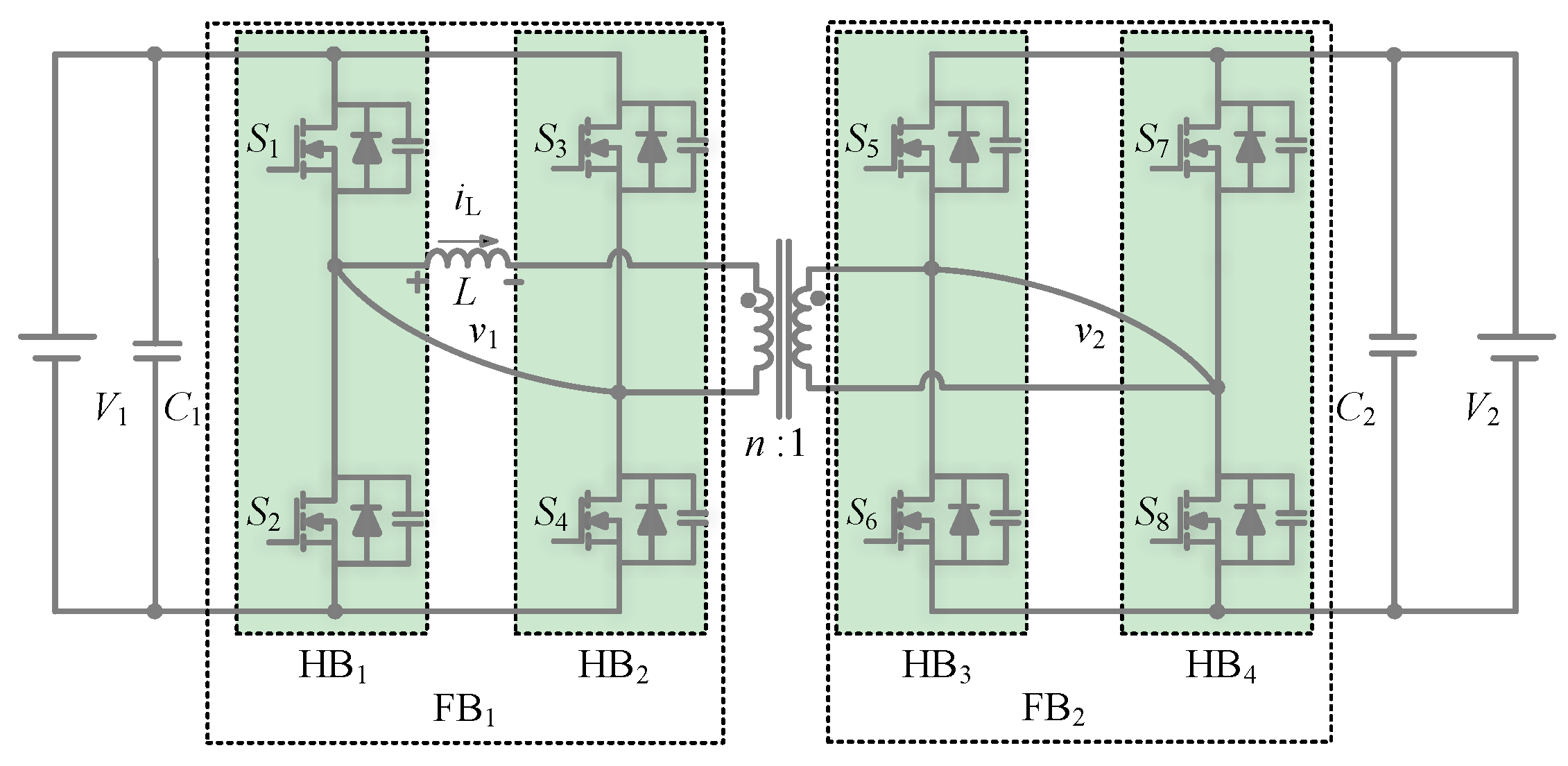
2.1. DAB Basic Topology
2.2. ZVS Conditions of DAB Converter
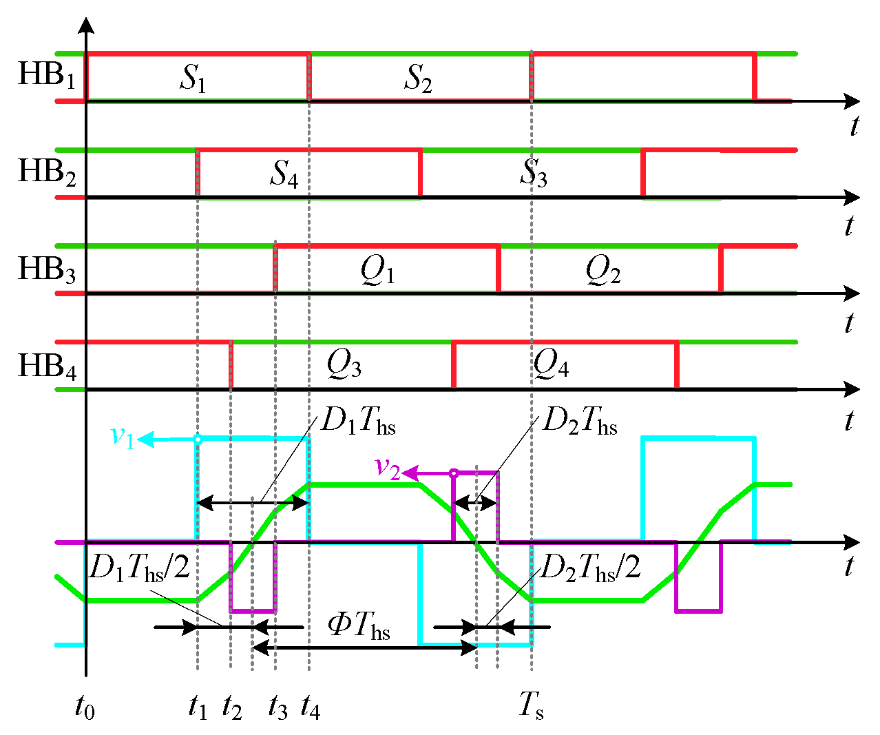
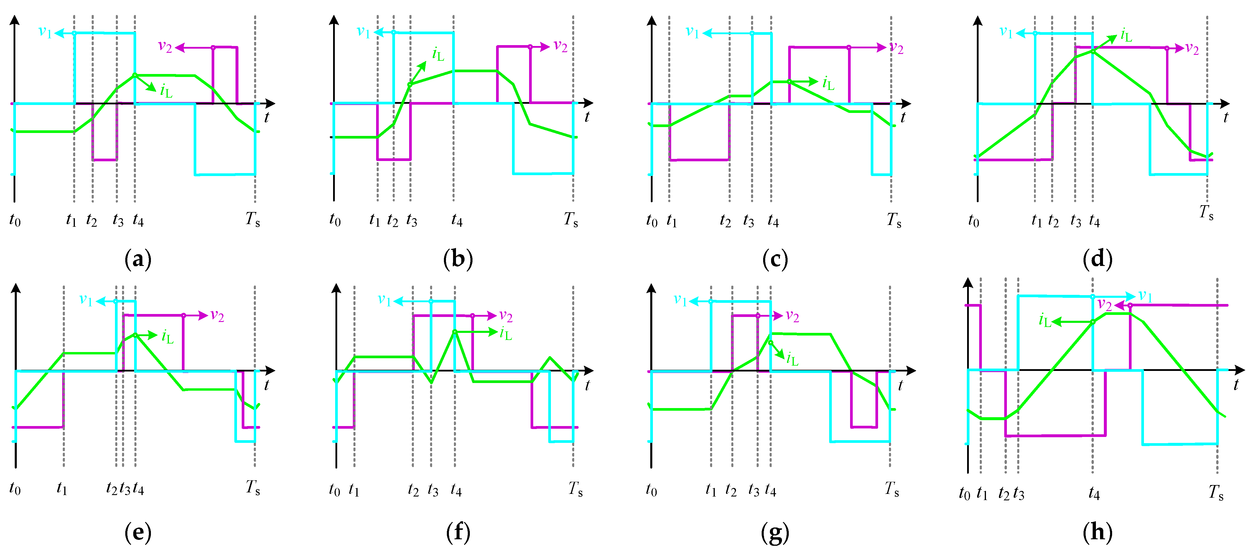
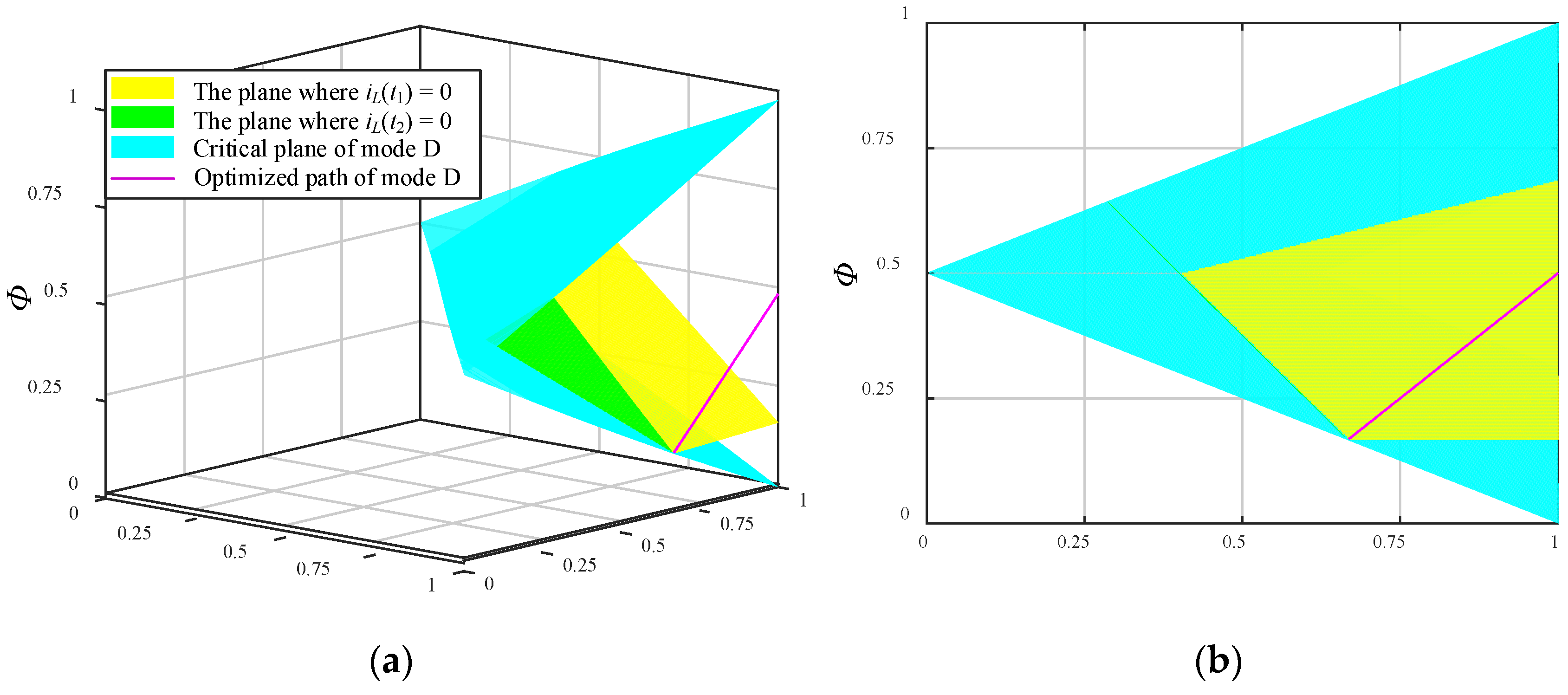
2.3. TPS Mode Classification and Mode Selection of the DAB Converter
3. Principle of the Proposed EIOS-TPS
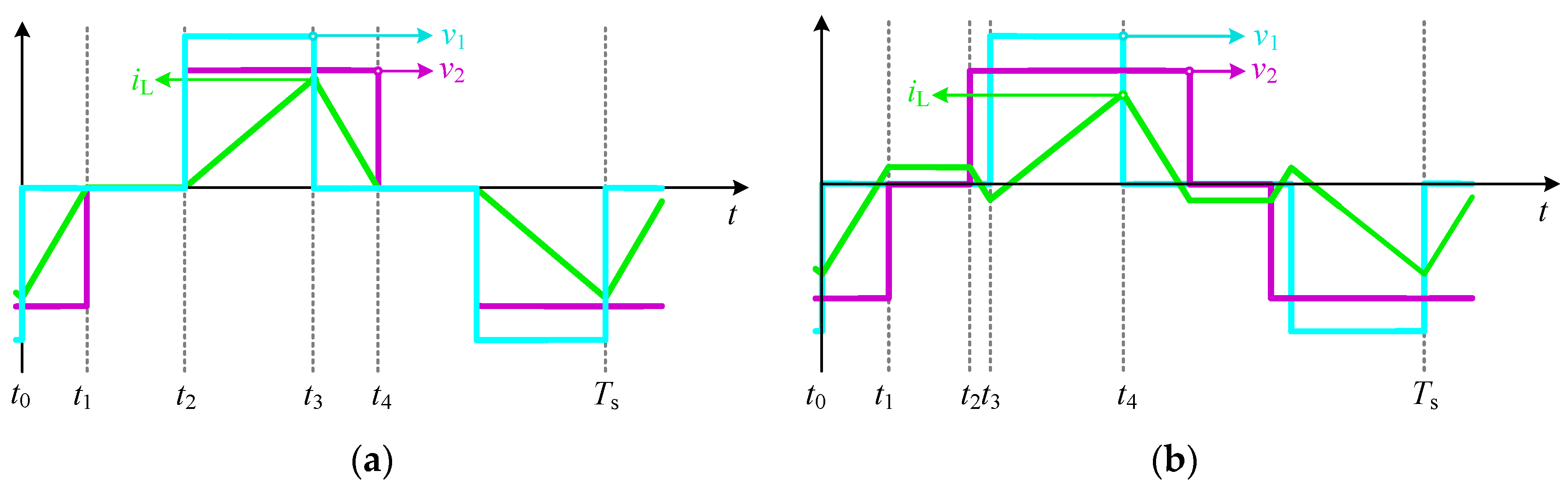
3.1. Modulation Strategy in the Low-Power Range When k > 1
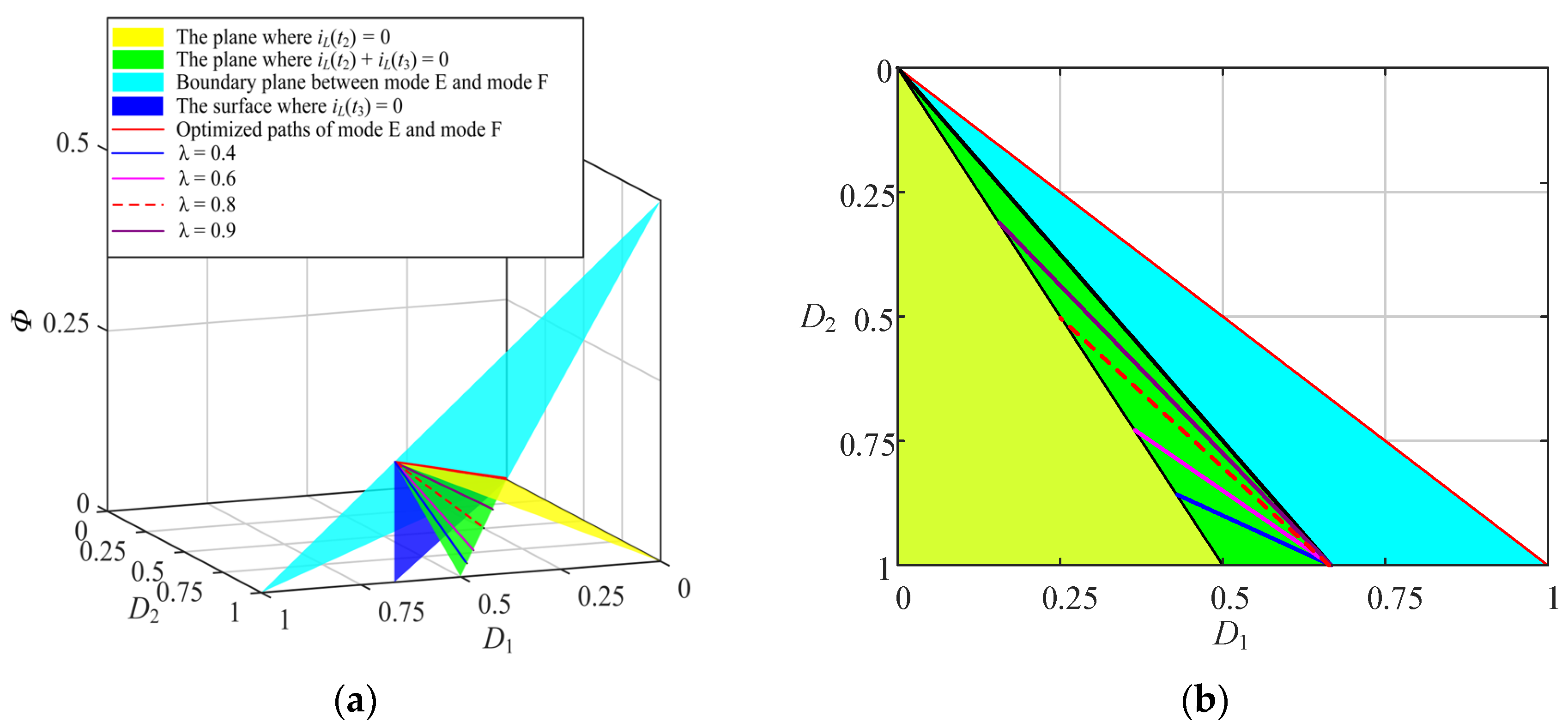
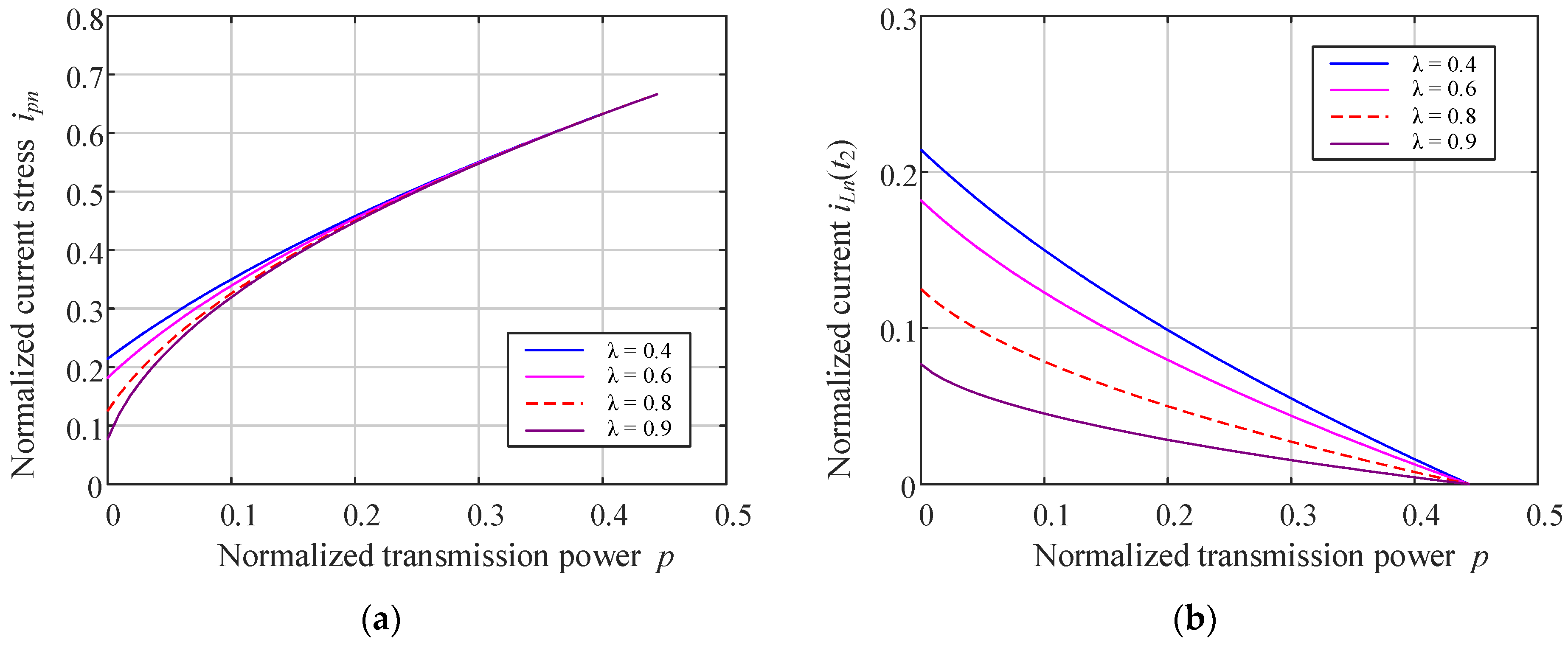
3.2. Modulation Strategy in the Medium and High-Power Range When k > 1
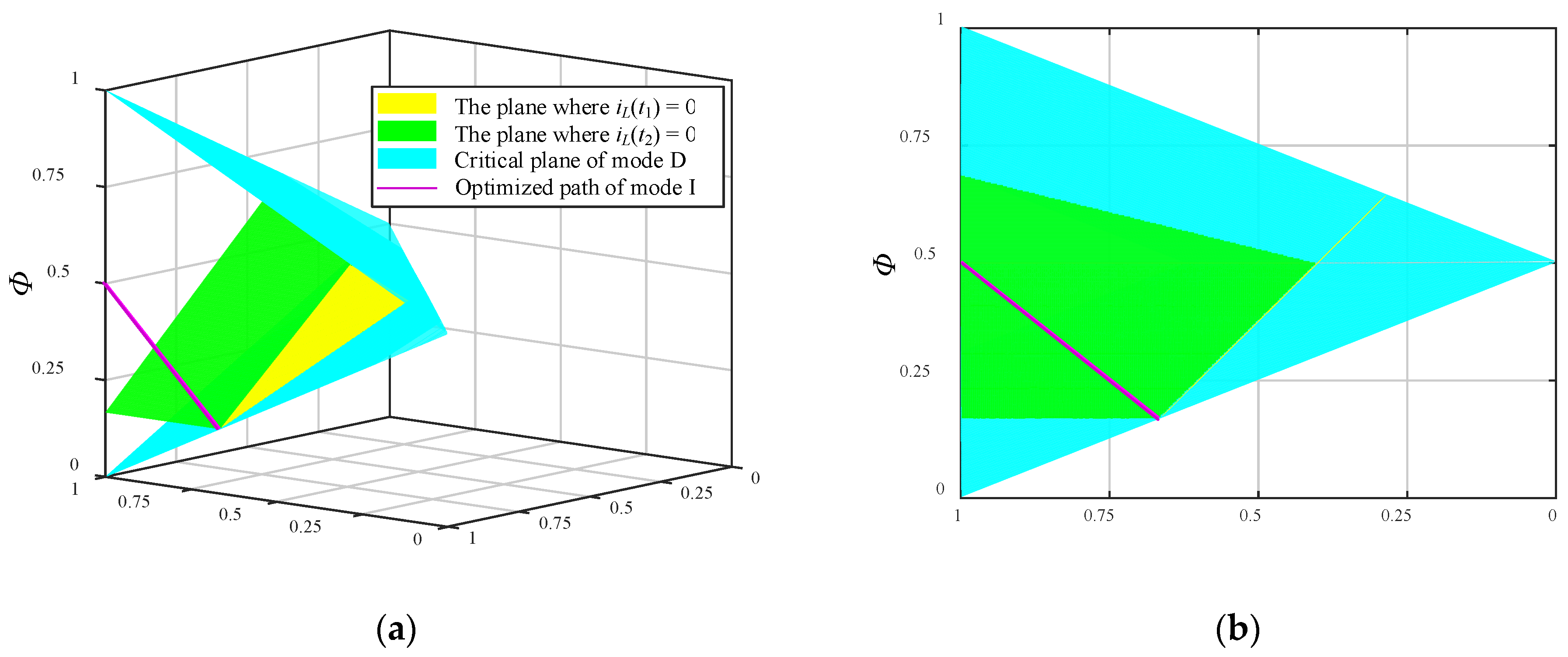
3.3. Modulation Strategy in the Low-Power Range When k < 1
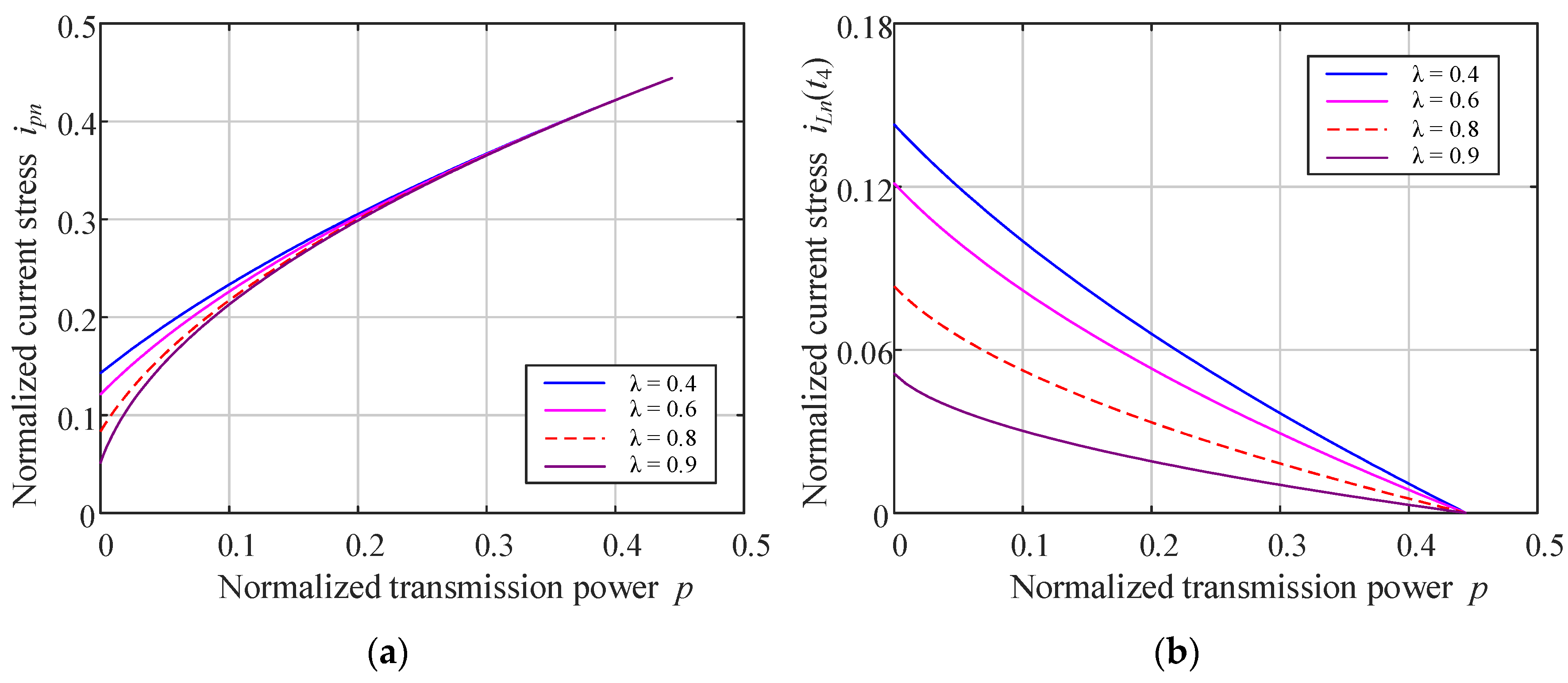
3.4. Modulation Strategy in the Medium and High-Power Range When k < 1
4. Simulation Comparison with Existing Schemes
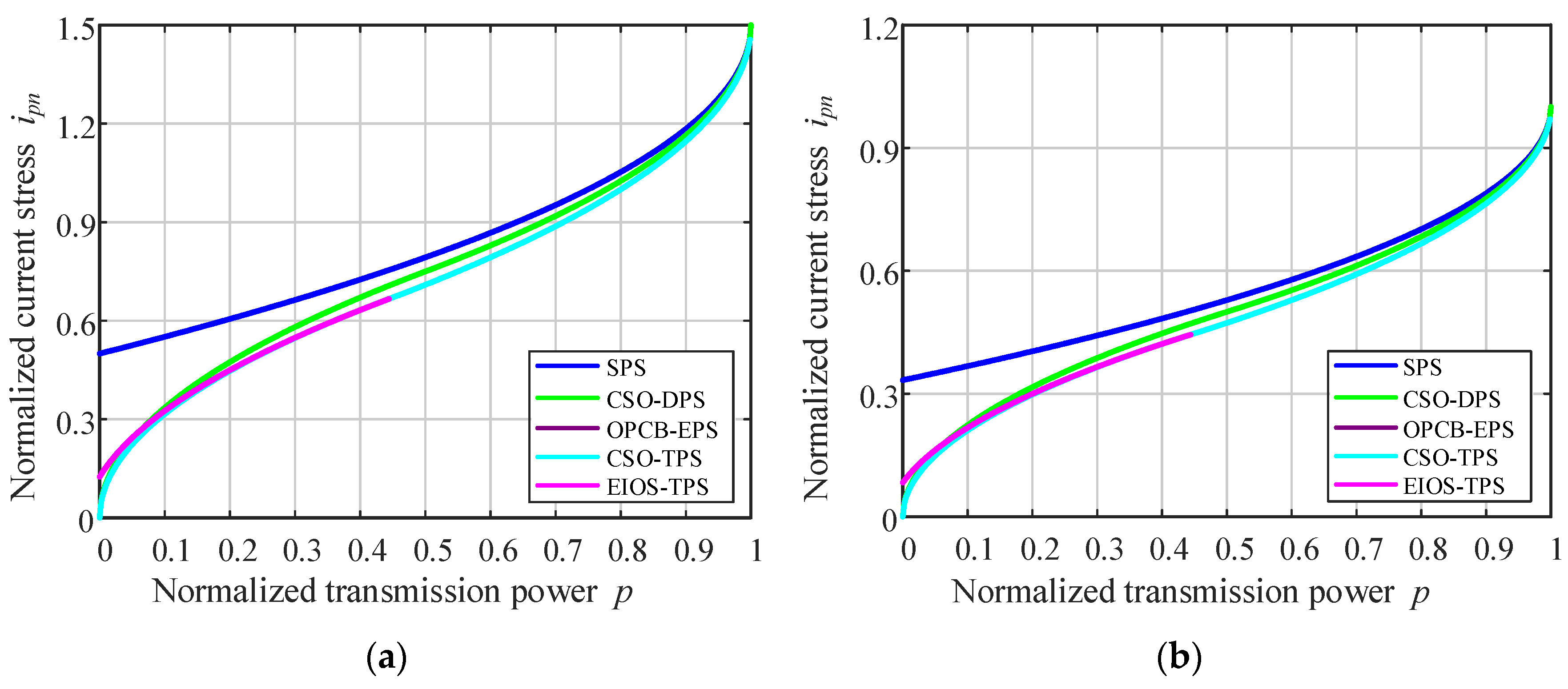
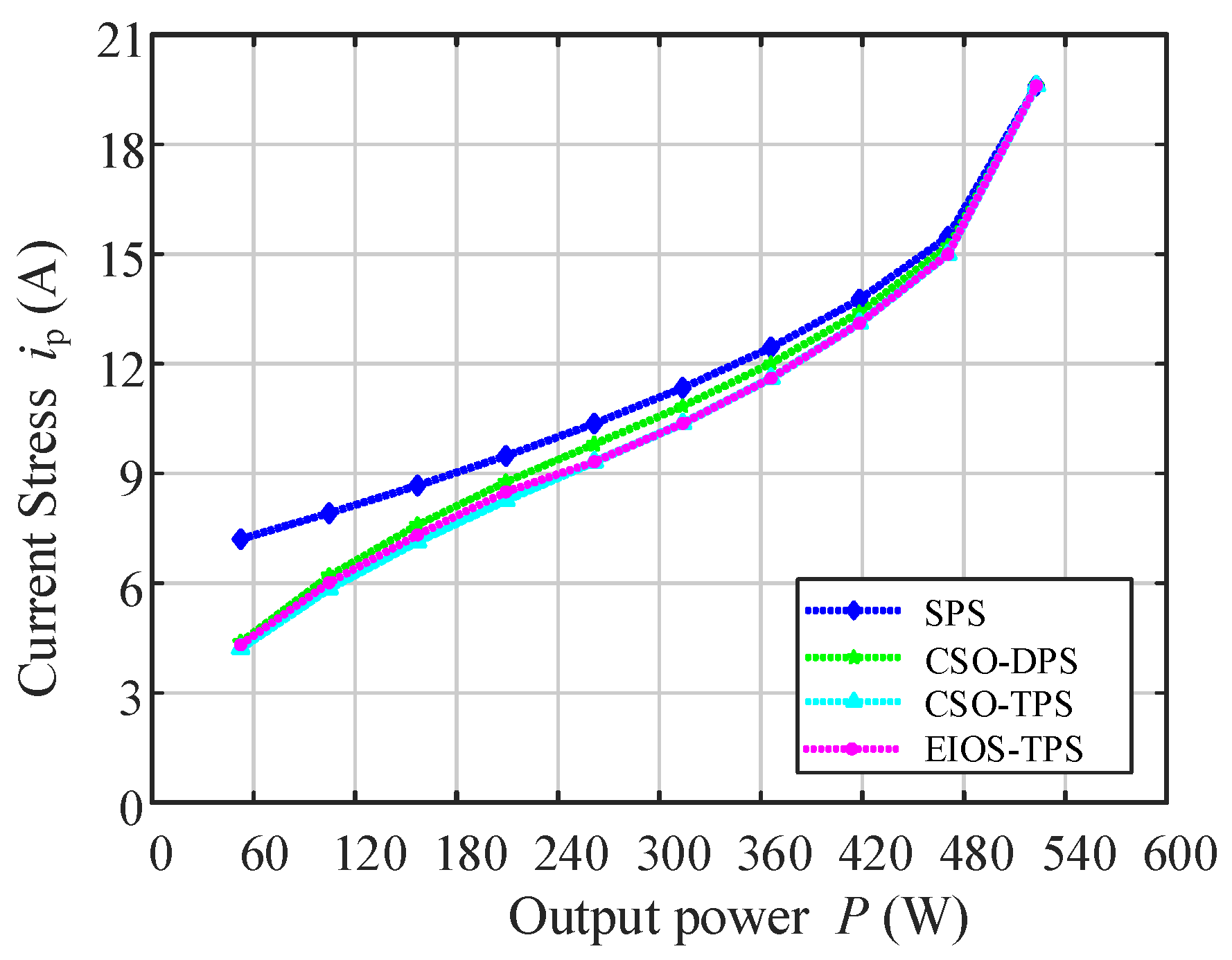
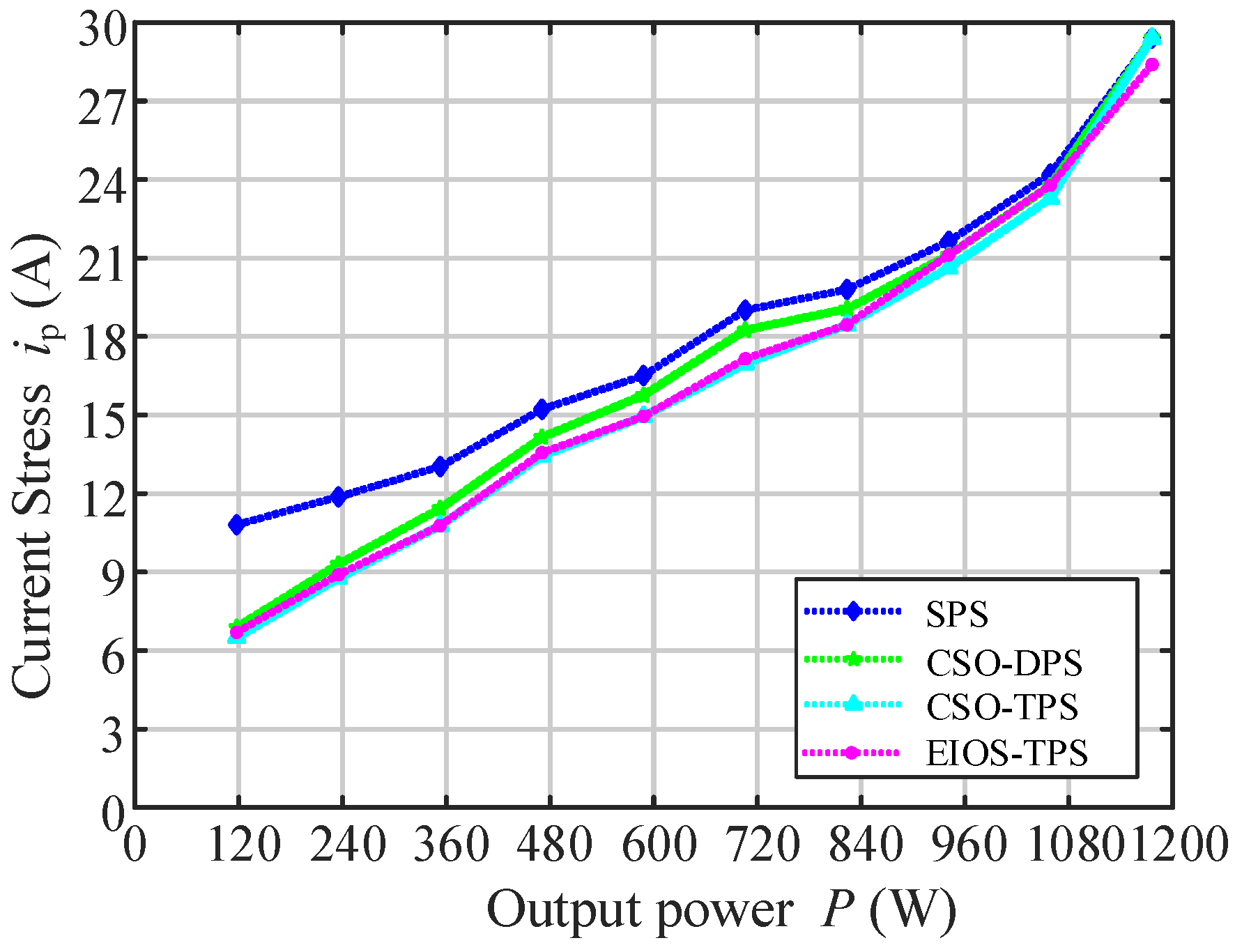
4.1. Current Stress
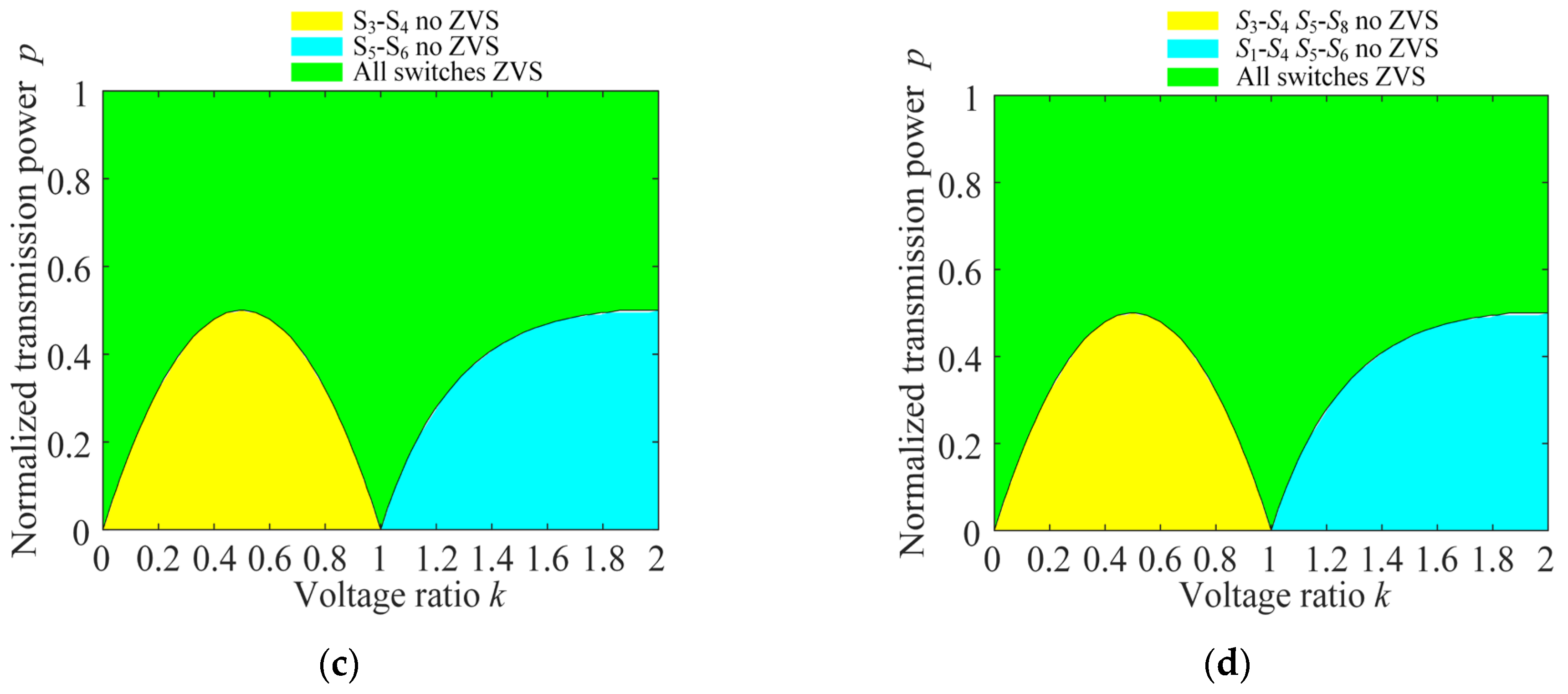
4.2. ZVS Range
5. Experimental Verification
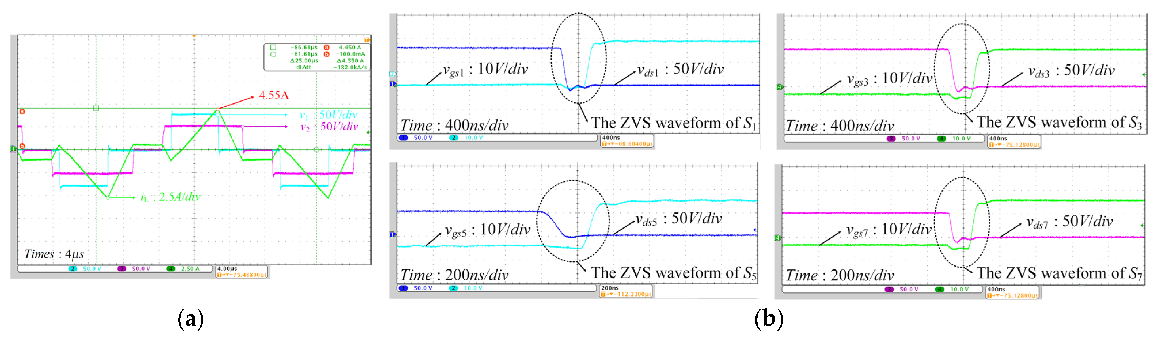
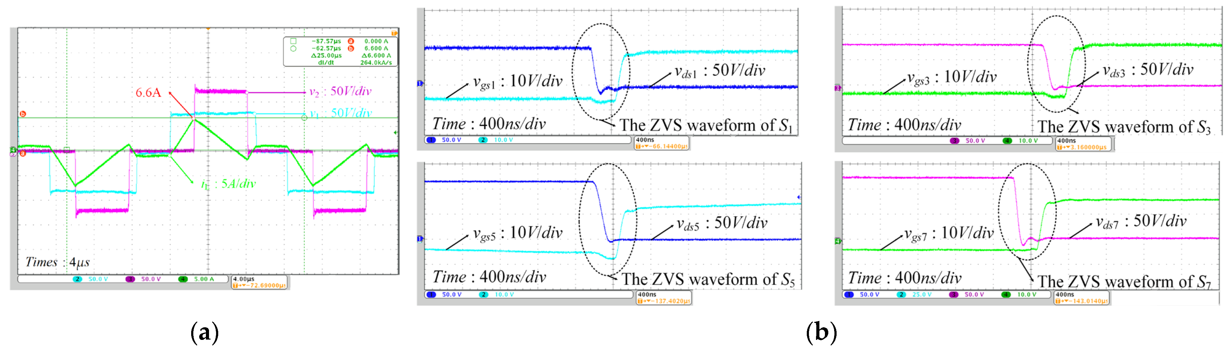
5.1. Experimental Verification with k > 1
5.2. Experimental Verification with k < 1
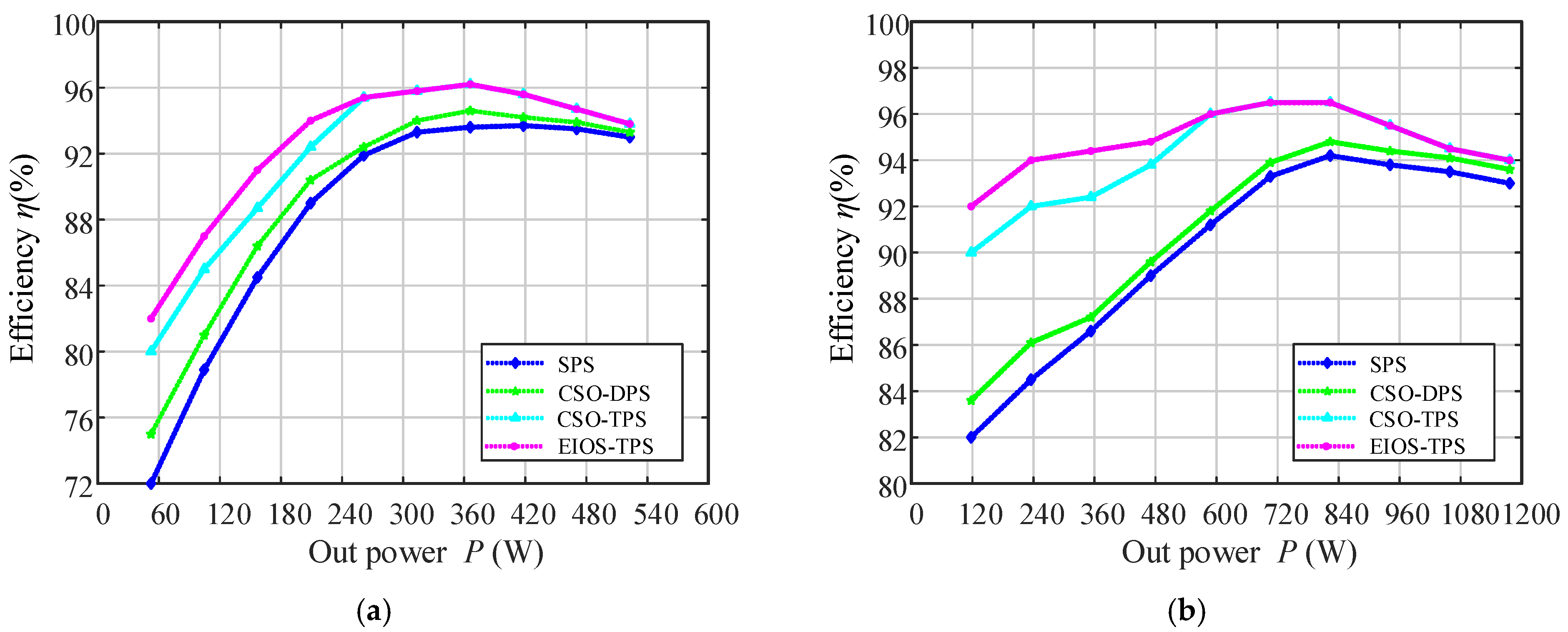
5.3. Efficiency
6. Conclusions
Author Contributions
Funding
Institutional Review Board Statement
Informed Consent Statement
Data Availability Statement
Conflicts of Interest
Abbreviations
| DAB | Dual-active bridge (converter) |
| ZVS | Zero-voltage switching |
| MCS | Minimizing current stress |
| EIOS-TPS | Enhanced Integrated Optimization Strategy based on triple phase shift |
| KKT | Karush–Kuhn–Tucker (conditions) |
| ZCS | Zero current switching |
| CSO | Current-stress optimization |
| RMSO | Root-mean-square current optimization |
| EB ZVS | Energy-based zero-voltage switching |
| CB ZVS | Current-based zero-voltage switching |
| QB ZVS | Charge-based zero-voltage switching |
| SPS | Single phase-shift modulation |
| DPS | Dual phase-shift modulation |
| EPS | Extended phase-shift modulation |
| TPS | Triple phase-shift modulation |
| LMM | Lagrange Multiplier Method |
| RL | Reinforcement learning |
| ANN | Artificial neural networks |
| AI | Artificial Intelligence |
| PSO | Particle swarm optimization |
| FIS | Fuzzy inference systems |
References
- Doncker, R.W.A.A.D.; Divan, D.M.; Kheraluwal, M.H. A Three-phase Soft-Switched High-Power-Density dc/dc Converter for High-Power Applications. IEEE Trans. Ind. Appl. 1991, 27, 63–73. [Google Scholar] [CrossRef]
- Zhao, B.; Song, Q.; Liu, W.; Xiao, Y. Next-Generation Multi-Functional Modular Intelligent UPS System for Smart Grid. IEEE Trans. Ind. Electron. 2013, 60, 3602–3618. [Google Scholar] [CrossRef]
- Zhao, B.; Song, Q.; Li, J.G.; Wang, Y.; Liu, W.H. High-Frequency-Link Modulation Methodology of DC-DC Transformer Based on Modular Multilevel Converter for HVDC Application: Comprehensive Analysis and Experimental Verification. IEEE Trans. Power Electron. 2017, 32, 3413–3424. [Google Scholar] [CrossRef]
- Xue, L.X.; Shen, Z.Y.; Boroyevich, D.; Mattavelli, P.; Diaz, D. Dual Active Bridge-Based Battery Charger for Plug-in Hybrid Electric Vehicle with Charging Current Containing Low Frequency Ripple. IEEE Trans. Power Electron. 2015, 30, 7299–7307. [Google Scholar] [CrossRef]
- Taylor, A.; Liu, G.L.; Bai, H.; Brown, A.; Johnson, P.M.; McAmmond, M. Multiple-Phase-Shift Control for a Dual Active Bridge to Secure Zero-Voltage Switching and Enhance Light-Load Performance. IEEE Trans. Power Electron. 2018, 33, 4584–4588. [Google Scholar] [CrossRef]
- Tan, N.M.L.; Abe, T.; Akagi, H. Design and Performance of a Bidirectional Isolated DC-DC Converter for a Battery Energy Storage System. IEEE Trans. Power Electron. 2012, 27, 1237–1248. [Google Scholar] [CrossRef]
- Karthikeyan, V.; Gupta, R. Multiple-Input Configuration of Isolated Bidirectional DC-DC Converter for Power Flow Control in Combinational Battery Storage. IEEE Trans. Ind. Inform. 2018, 14, 2–11. [Google Scholar] [CrossRef]
- Naayagi, R.T.; Forsyth, A.J.; Shuttleworth, R. Bidirectional control of a dual active bridge DC-DC converter for aerospace applications. IET Power Electron. 2012, 5, 1104–1118. [Google Scholar] [CrossRef]
- Hou, N.; Li, Y.W. Overview and Comparison of Modulation and Control Strategies for a Nonresonant Single-Phase Dual-Active-Bridge DC-DC Converter. IEEE Trans. Power Electron. 2020, 35, 3148–3172. [Google Scholar] [CrossRef]
- Shao, S.; Chen, L.L.; Shan, Z.Y.; Gao, F.; Chen, H.; Sha, D.S.; Dragicevic, T. Modeling and Advanced Control of Dual-Active-Bridge DC-DC Converters: A Review. IEEE Trans. Power Electron. 2022, 37, 1524–1547. [Google Scholar] [CrossRef]
- Chaurasiya, S.; Singh, B. A Load Adaptive Hybrid DPS Control for DAB to Secure Minimum Current Stress and Full ZVS Operation Over Wide Load and Voltage Conversion Ratio. IEEE Trans. Ind. Appl. 2023, 59, 1901–1911. [Google Scholar] [CrossRef]
- Krismer, F.; Kolar, J.W. Accurate Power Loss Model Derivation of a High-Current Dual Active Bridge Converter for an Automotive Application. IEEE Trans. Ind. Electron. 2010, 57, 881–891. [Google Scholar] [CrossRef]
- Shi, H.; Wen, H.; Hu, Y. Deadband Effect and Accurate ZVS Boundaries of GaN-Based Dual-Active-Bridge Converters with Multiple-Phase-Shift Control. IEEE Trans. Power Electron. 2020, 35, 9886–9903. [Google Scholar] [CrossRef]
- Hou, N.; Song, W.S.; Wu, M.Y. Minimum-Current-Stress Scheme of Dual Active Bridge DC-DC Converter With Unified Phase-Shift Control. IEEE Trans. Power Electron. 2016, 31, 8552–8561. [Google Scholar] [CrossRef]
- Huang, J.; Wang, Y.; Li, Z.; Lei, W. Unified Triple-Phase-Shift Control to Minimize Current Stress and Achieve Full Soft-Switching of Isolated Bidirectional DC-DC Converter. IEEE Trans. Ind. Electron. 2016, 63, 4169–4179. [Google Scholar] [CrossRef]
- Gu, Q.; Yuan, L.; Nie, J.; Sun, J.; Zhao, Z. Current Stress Minimization of Dual-Active-Bridge DC-DC Converter Within the Whole Operating Range. IEEE J. Emerg. Sel. Top. Power Electron. 2019, 7, 129–142. [Google Scholar] [CrossRef]
- Oggier, G.G.; Garcia, G.O.; Oliva, A.R. Modulation Strategy to Operate the Dual Active Bridge DC-DC Converter Under Soft Switching in the Whole Operating Range. IEEE Trans. Power Electron. 2011, 26, 1228–1236. [Google Scholar] [CrossRef]
- Li, S.; Yuan, X.; Wang, Z.; Wang, K.; Zhang, Y.; Wu, X. A Unified Optimal Modulation Strategy for DAB Converters to Tradeoff the Backflow Power Reduction and All ZVS in the Full Operating Range. IEEE J. Emerg. Sel. Top. Power Electron. 2023, 11, 5701–5723. [Google Scholar] [CrossRef]
- Krismer, F.; Kolar, J.W. Closed Form Solution for Minimum Conduction Loss Modulation of DAB Converters. IEEE Trans. Power Electron. 2012, 27, 174–188. [Google Scholar] [CrossRef]
- Everts, J.; Krismer, F.; Van den Keybus, J.; Driesen, J.; Kolar, J.W. Optimal ZVS Modulation of Single-Phase Single-Stage Bidirectional DAB AC-DC Converters. IEEE Trans. Power Electron. 2014, 29, 3954–3970. [Google Scholar] [CrossRef]
- Yang, X.; Wang, J.; Du, Y.; Liu, C.; Zhang, T.; Zhang, J. Bidirectional ZVS Operation of All Switches for a DAB Converter Over a Full Range of Loads With Optimized Current Stress. IEEE Trans. Ind. Appl. 2024, 60, 1183–1195. [Google Scholar] [CrossRef]
- Kasper, M.; Burkart, R.M.; Deboy, G.; Kolar, J.W. ZVS of Power MOSFETs Revisited. IEEE Trans. Power Electron. 2016, 31, 8063–8067. [Google Scholar] [CrossRef]
- Yan, Y.; Gui, H.D.; Bai, H. Complete ZVS Analysis in Dual Active Bridge. IEEE Trans. Power Electron. 2021, 36, 1247–1252. [Google Scholar] [CrossRef]
- Tao, H.; Kotsopoulos, A.; Duarte, J.L.; Hendrix, M.A.M. Transformer-coupled multiport ZVS bidirectional DC-DC converter with wide input range. IEEE Trans. Power Electron. 2008, 23, 771–781. [Google Scholar] [CrossRef]
- Wang, Z.; Li, C.; Liu, J.Y.; Zheng, Z.D. Influence of Junction-Capacitance and Dead-Time on Dual-Active-Bridge Actual Soft-Switching-Range: Analytic Analysis and Solution. IEEE Trans. Power Electron. 2023, 38, 6157–6168. [Google Scholar] [CrossRef]
- Fan, Z.H.; Lu, H.F.; Chai, J.Y.; Li, Y.W.; Sun, X.D. Partition Variable Frequency and EPS Hybrid Control to Achieve Full Load Range ZVS for Dual Active Bridge Converters. IEEE J. Emerg. Sel. Top. Power Electron. 2024, 12, 143–155. [Google Scholar] [CrossRef]
- Xu, G.; Sha, D.S.; Xu, Y.X.; Liao, X.Z. Dual-Transformer-Based DAB Converter With Wide ZVS Range for Wide Voltage Conversion Gain Application. IEEE Trans. Ind. Electron. 2018, 65, 3306–3316. [Google Scholar] [CrossRef]
- Guo, Z.; Sha, D. Dual-Active-Bridge Converter With Parallel-Connected Full Bridges in Low-Voltage Side for ZVS by Using Auxiliary Coupling Inductor. IEEE Trans. Ind. Electron. 2019, 66, 6856–6866. [Google Scholar] [CrossRef]
- Zhao, B.; Song, Q.; Liu, W.; Liu, G.; Zhao, Y. Universal High-Frequency-Link Characterization and Practical Fundamental-Optimal Strategy for Dual-Active-Bridge DC-DC Converter Under PWM Plus Phase-Shift Control. IEEE Trans. Power Electron. 2015, 30, 6488–6494. [Google Scholar] [CrossRef]
- Xie, H.; Cai, F.; Jiang, J.; Li, D. A Fundamental Harmonic Analysis-Based Optimized Scheme for DAB Converters With Lower RMS Current and Wider ZVS Range. IEEE Trans. Transp. Electrif. 2023, 9, 4045–4058. [Google Scholar] [CrossRef]
- Zhao, B.; Yu, Q.; Sun, W. Extended-Phase-Shift Control of Isolated Bidirectional DC-DC Converter for Power Distribution in Microgrid. IEEE Trans. Power Electron. 2012, 27, 4667–4680. [Google Scholar] [CrossRef]
- Yu, H.; Hang, L.; Zheng, X.; He, Z.; He, Y.; Shen, L.; Shao, C.; Zeng, P.; Wu, Q.; Yang, X.; et al. Globally Unified ZVS and Quasi-Optimal Minimum Conduction Loss Modulation of DAB Converters. IEEE Trans. Transp. Electrif. 2022, 8, 3989–4000. [Google Scholar] [CrossRef]
- Zhao, B.; Song, Q.; Liu, W. Efficiency Characterization and Optimization of Isolated Bidirectional DC-DC Converter Based on Dual-Phase-Shift Control for DC Distribution Application. IEEE Trans. Power Electron. 2013, 28, 1711–1727. [Google Scholar] [CrossRef]
- Liu, X.; Zhu, Z.Q.; Stone, D.A.; Foster, M.P.; Chu, W.Q.; Urquhart, I.; Greenough, J. Novel Dual-Phase-Shift Control With Bidirectional Inner Phase Shifts for a Dual-Active-Bridge Converter Having Low Surge Current and Stable Power Control. IEEE Trans. Power Electron. 2017, 32, 4095–4106. [Google Scholar] [CrossRef]
- Zhao, B.; Song, Q.; Liu, W.; Sun, W. Current-Stress-Optimized Switching Strategy of Isolated Bidirectional DC-DC Converter with Dual-Phase-Shift Control. IEEE Trans. Ind. Electron. 2013, 60, 4458–4467. [Google Scholar] [CrossRef]
- Li, L.T.; Xu, G.; Xiong, W.J.; Liu, D.; Su, M. An Optimized DPS Control for Dual-Active-Bridge Converters to Secure Full-Load-Range ZVS With Low Current Stress. IEEE Trans. Transp. Electrif. 2022, 8, 1389–1400. [Google Scholar] [CrossRef]
- An, F.; Song, W.S.; Yu, B.; Yang, K.X. Model Predictive Control With Power Self-Balancing of the Output Parallel DAB DC-DC Converters in Power Electronic Traction Transformer. IEEE J. Emerg. Sel. Top. Power Electron. 2018, 6, 1806–1818. [Google Scholar] [CrossRef]
- An, F.; Song, W.; Yang, K.; Luo, S.; Feng, X. Optimised power control and balance scheme for the output parallel dual-active-bridge DC-DC converters in power electronic traction transformer. IET Power Electron. 2019, 12, 2295–2303. [Google Scholar] [CrossRef]
- Xu, F.; Liu, J.W.; Dong, Z. Minimum Backflow Power and ZVS Design for Dual-Active-Bridge DC-DC Converters. IEEE Trans. Ind. Electron. 2023, 70, 474–484. [Google Scholar] [CrossRef]
- Zhang, Y.; Zong, J.; Zhang, F.; Li, X.; Wei, Y.; Ma, H. A Comprehensive Optimization Strategy of DAB Converter with Minimal Current Stress and Full Soft Switching in the Whole Operating Range. IEEE J. Emerg. Sel. Top. Power Electron. 2024, 12, 129–142. [Google Scholar] [CrossRef]
- Li, J.; Luo, Q.M.; Mou, D.; Wei, Y.Q.; Zhang, X.Y. Comprehensive Optimization Modulation Scheme of Low Current Level and Wide ZVS Range for Dual Active Bridge Converter With Dead-Zone Control. IEEE Trans. Power Electron. 2022, 37, 2731–2748. [Google Scholar] [CrossRef]
- Tang, Y.; Hu, W.; Xiao, J.; Lu, Z.; Li, Z.; Huang, Q.; Chen, Z.; Blaabjerg, F. RL-ANN-Based Minimum-Current-Stress Scheme for the Dual-Active-Bridge Converter With Triple-Phase-Shift Control. IEEE J. Emerg. Sel. Top. Power Electron. 2022, 10, 673–689. [Google Scholar] [CrossRef]
- Li, X.; Zhang, X.; Lin, F.; Sun, C.; Mao, K. Artificial-Intelligence-Based Triple Phase Shift Modulation for Dual Active Bridge Converter with Minimized Current Stress. IEEE J. Emerg. Sel. Top. Power Electron. 2023, 11, 4430–4441. [Google Scholar] [CrossRef]
- Naseem, H.; Seok, J.-K. Reactive Power Controller for Single Phase Dual Active Bridge DC–DC Converters. IEEE Access 2023, 11, 141537–141546. [Google Scholar] [CrossRef]
- Zhang, J.; Sha, D.; Song, K. Single-Phase Single-Stage Bidirectional DAB AC-DC Converter with Extended ZVS Range and High Efficiency. IEEE Trans. Power Electron. 2023, 38, 3803–3811. [Google Scholar] [CrossRef]
- Tian, J.; Wang, F.; Zhuo, F.; Cui, X.; Yang, D. An Optimal Primary-Side Duty Modulation Scheme with Minimum Peak-to-Peak Current Stress for DAB-Based EV Applications. IEEE Trans. Ind. Electron. 2023, 70, 6798–6808. [Google Scholar] [CrossRef]
- Wang, X.; Yang, M.; Sima, W.; Yuan, T.; Sun, P.; Lin, S. Composite Duty Modulation of Dual Active Bridge Converters to Minimize Output Voltage Ripples and Inductor RMS Currents. IEEE Trans. Power Electron. 2024, 39, 5662–5681. [Google Scholar] [CrossRef]
- Zhang, L.; Tu, C.; Xiao, F.; Liu, B.; Li, P. Intrinsic Regularity Analysis and Optimization Control of Current Stress and RMS for Dual-Active Bridge Converter. Electronics 2024, 13, 4802. [Google Scholar] [CrossRef]
- Yan, Y.; Luo, Q.; Luo, T.; Li, J.; Xiong, J.; Xiao, H. Current Stress Optimized Strategy for the Dual-Active-Bridge Converter with Triple-Phase-Shift and Variable DC-Link Voltage Control. IEEE Trans. Power Electron. 2025, 40, 8344–8355. [Google Scholar] [CrossRef]


| Polarity of the Inductor Current | Switches |
|---|---|
| iL < 0 | S1, S4, S6, S7 |
| iL > 0 | S2, S3, S5, S8 |
| Mode | Mode Constraints | Expression of Normalized Transmitted Power p | Range of p |
|---|---|---|---|
| A | [0, 0.5] | ||
| B | [0, 0.5] | ||
| C | [0, 0.5] | ||
| D | [0, 1] | ||
| E | [0, 0.666] | ||
| F | [0, 0.5] | ||
| G | [0, 0.5] | ||
| H | [0, 0.5] |
| Mode | iLn(t0) | iLn(t1) | iLn(t2) | iLn(t3) | iLn(t4) |
|---|---|---|---|---|---|
| D | |||||
| E | |||||
| F | |||||
| G |
| Mode | Maximum Current Stress When k > 1 | Maximum Current Stress When k < 1 |
|---|---|---|
| D | ||
| E | ||
| F | ||
| G |
| Circuit Parameters | Specifications |
|---|---|
| Power | Input Voltage V1 = 80 V |
| Output Voltage V2 = 53.33 V, 120 V | |
| Maximum Power Pmax = 1176 W | |
| Switching Frequency fs = 40 kHz | |
| Transformer Turns Ratio n = 1 | |
| Inductor L = 25.5 µH | |
| Switch | S1–S4, S5–S8: C3M0075120K VDSS = 1200 V, ID = 32 A, Rds(on) = 40 mΩ, Coss = 58 pF |
| SiC MOSFET Drivers | 1EDI60N12AF |
| Microcontroller | TMS320F28335 |
| Filter Capacitor (C1, C2) | Input Capacitor C1 = 450 µF Output Capacitor C2 = 450 µF |
Disclaimer/Publisher’s Note: The statements, opinions and data contained in all publications are solely those of the individual author(s) and contributor(s) and not of MDPI and/or the editor(s). MDPI and/or the editor(s) disclaim responsibility for any injury to people or property resulting from any ideas, methods, instructions or products referred to in the content. |
© 2025 by the authors. Licensee MDPI, Basel, Switzerland. This article is an open access article distributed under the terms and conditions of the Creative Commons Attribution (CC BY) license (https://creativecommons.org/licenses/by/4.0/).
Share and Cite
Cui, L.; Zhang, Y.; Wang, X.; Zhang, D. An Enhanced Integrated Optimization Strategy for Wide ZVS Operation and Reduced Current Stress Across the Full Load Range in DAB Converters. Appl. Sci. 2025, 15, 7413. https://doi.org/10.3390/app15137413
Cui L, Zhang Y, Wang X, Zhang D. An Enhanced Integrated Optimization Strategy for Wide ZVS Operation and Reduced Current Stress Across the Full Load Range in DAB Converters. Applied Sciences. 2025; 15(13):7413. https://doi.org/10.3390/app15137413
Chicago/Turabian StyleCui, Longfei, Yiming Zhang, Xuhong Wang, and Dong Zhang. 2025. "An Enhanced Integrated Optimization Strategy for Wide ZVS Operation and Reduced Current Stress Across the Full Load Range in DAB Converters" Applied Sciences 15, no. 13: 7413. https://doi.org/10.3390/app15137413
APA StyleCui, L., Zhang, Y., Wang, X., & Zhang, D. (2025). An Enhanced Integrated Optimization Strategy for Wide ZVS Operation and Reduced Current Stress Across the Full Load Range in DAB Converters. Applied Sciences, 15(13), 7413. https://doi.org/10.3390/app15137413