Article

Surface Charge and Electric Field Distribution of Direct-Current Gas-Insulated Transmission Lines’ Basin-Type Insulators Under Multi-Field Coupling

School of Electrical Engineering, Shenyang University of Technology, Shenyang 110870, China
*
Author to whom correspondence should be addressed.
Appl. Sci. 2025, 15(13), 7061; https://doi.org/10.3390/app15137061
Submission received: 21 May 2025 / Revised: 19 June 2025 / Accepted: 19 June 2025 / Published: 23 June 2025
(This article belongs to the Special Issue Advances in Electrical Insulation Systems)

Abstract

In direct-current gas-insulated transmission lines (DC GIL), complex heat transfer processes accelerate surface charge accumulation on insulators, causing local electric field distortion and elevating the risk of surface flashover. This study develops a three-dimensional multi-physics coupled mathematical model for ±200 kV DC GIL basin-type insulators. The bulk and surface conductivity of insulator materials were experimentally measured under varying temperature and electric field conditions, with fitting equations derived to describe their behavior. The model investigates surface charge accumulation and electric field distribution under DC voltage and polarity-reversal conditions, incorporating multi-field coupling effects. Results show that, at a 3150 A current in a horizontally arranged DC GIL, insulator temperatures reach approximately 62.8 °C near the conductor and 32 °C near the enclosure, with the convex surface exhibiting higher temperatures than the concave surface and distinct radial variations. Under DC voltage, surface charge accumulates faster in high-temperature regions, with both charge and electric field distributions stabilizing after approximately 300 h, following significant changes within the first 40 h. Following stabilization, the distribution of surface charge and electric field varies across different radial directions. During polarity reversal, residual surface charges cause electric field distortion, increasing maximum field strength by 13.6% and 47.2% on the convex and concave surfaces, respectively, with greater distortion on the concave surface, as calculated from finite element simulations with a numerical accuracy of ±0.5% based on mesh convergence and solver tolerance. These findings offer valuable insights for enhancing DC GIL insulation performance.

1. Introduction

Gas-insulated transmission lines (GILs) are extensively employed in electric energy transmission systems due to their exceptional reliability and substantial power transfer capacity [1]. As an innovative reserve technology, direct current (DC) GIL efficiently utilizes limited spatial resources while playing a pivotal role in the development of future power transmission networks characterized by large capacity and long-distance capabilities [2]. Under DC voltage, charge accumulation in high-voltage direct current (HVDC) cables and gas-insulated systems markedly distorts electric field distributions, compromising insulation performance and increasing the risk of dielectric breakdown [3,4]. Similarly, this charge-induced distortion influences the electric field distribution of GIL, which gradually transitions from an initial capacitive field to a resistive field, with surface charge accumulation on the insulator further exacerbating electric field distortion [5]. When voltage polarity reversal occurs, the local electric field distortion caused by surface charge accumulation becomes particularly pronounced [6]. Furthermore, under high-voltage and high-current operating conditions of DC GIL, the combined influence of electric and thermal fields exacerbates surface charge accumulation, consequently intensifying local electric field distortion [7,8]. Therefore, investigating the characteristics of insulator surface charge accumulation and electric field distribution under multi-physical field coupling is crucial for improving the insulation performance of DC GIL and enhancing overall system stability.
In recent years, with the continual advancement of high-voltage DC transmission capacity and voltage levels, the gas–solid insulation systems of DC GIL have encountered increasingly severe challenges [9]. Charge accumulation on insulator surfaces is widely recognized as a key factor affecting electric field distribution and subsequently elevating the risk of insulation failure [10]. Particularly under polarity-reversal voltage, residual charge preceding the reversal can trigger local electric field distortion, thereby significantly compromising the safe and reliable operation of power equipment [11]. Consequently, researchers have conducted extensive and rigorous investigations to improve the insulation performance of DC GIL. Studies have demonstrated that charge accumulation on insulator surfaces is primarily influenced by material conductivity, gas conductivity, and interfacial charge transport [5,12]. In actual operation, the distribution of electric and thermal fields significantly alters the conductivity characteristics of insulator materials and the migration and diffusion behavior of charged particles in the gas medium, thereby exacerbating surface charge accumulation and resulting in distortion of the electric field along the surface [13,14]. Zhang et al. experimentally measured the surface charge distribution using a scaled-down insulator model under an electro-thermal coupling field [15]. However, due to limitations in measurement techniques, conducting accurate measurements of insulator surface charge accumulation under real operating conditions remains a significant challenge [16]. In contrast, numerical simulation methods offer superior flexibility. With advancements in computational science, simulation techniques have become increasingly mature and reliable, providing significant advantages for investigating transient characteristics of insulator surface charge accumulation and electric field distributions that are difficult to capture experimentally [17,18]. Ma et al. investigated the effect of volumetric conductivity on surface charge distribution and transient potential changes using finite element method (FEM) simulations [19]. Luo et al. constructed a two-dimensional axisymmetric surface charge accumulation model to investigate the dynamic characteristics of surface charge and electric field distribution along the GIL basin insulator surfaces under polarity-reversal voltage [20]. Yan et al. investigated the time-varying characteristics of insulator surface charge distribution, and the results verified that bulk conductivity can be greatly affected by temperature, which leads to an increase in insulator surface charge density [21]. Li et al. investigated insulator surface charge and electric field distribution under DC voltage through a three-dimensional electro–thermal coupling model for DC GIL, concluding that temperature distribution further aggravates electric field distortion along the surface [22,23]. Zheng et al. [24] examined the dynamics of spatial charge and electric field distributions in HVDC cables under temperature gradients and polarity-reversal conditions. However, within the existing literature, few scholars have addressed the effect of voltage polarity reversal on insulator surface charge and surface electric field distribution under multi-physics field coupling. It should be noted that in numerical simulations, differences between insulator body conductance and surface conductance parameters significantly impact calculation results [19,25]. Moreover, insulators are typically composed of epoxy resin matrix filled with metal oxide particles, particularly alumina. Different manufacturers employ varying material selection, filling ratios, and casting processes for filler particles, which directly influence the conductivity performance of insulators [26]. Therefore, the precise determination of insulator conductivity parameters through experimental methodologies is crucial for elucidating the charge accumulation and electric field distribution characteristics of DC GIL insulator surfaces under multi-physical field coupling, thereby significantly enhancing the reliability of subsequent investigations.
Research on surface charge accumulation in DC GIL basin-type insulators under multi-physics coupling conditions remains limited. Existing studies often lack experimental data on insulator material conductivity, and further exploration is needed to understand surface charge accumulation and electric field distribution during voltage polarity reversal under multi-physics interactions. This study addresses these gaps by experimentally measuring the bulk and surface conductivity of insulators across a range of temperatures and electric field strengths, deriving corresponding fitting equations. Additionally, a three-dimensional thermal–fluid–electrical multi-physics coupled model for DC GIL is developed to systematically analyze surface charge accumulation and electric field distribution under DC voltage and polarity-reversal conditions. These findings provide a robust theoretical framework and technical guidance for optimizing the design and enhancing the performance of DC GIL insulators.

2. Multi-Physics Coupling Mathematical Model

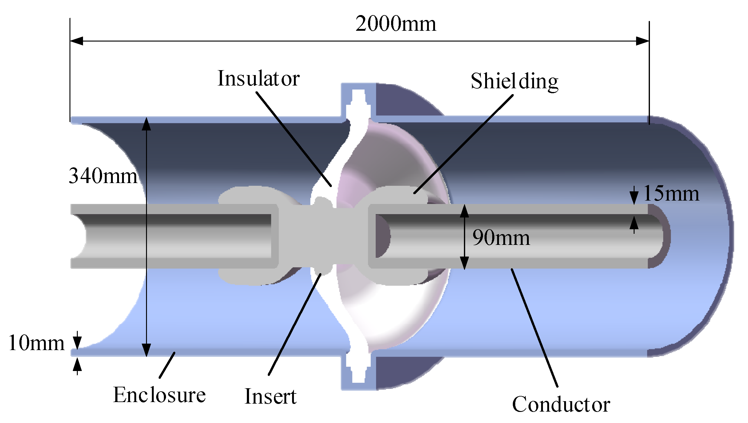
2.1. Geometric Model of DC GIL

The geometric model of the ±200 kV DC GIL, depicted in Figure 1, has a total length of 2 m. The central conductor, made of a 6101-T6 aluminum alloy, has an outer diameter of 90 mm and a wall thickness of 15 mm. The enclosure, constructed from a ZL101 aluminum alloy, features an outer diameter of 340 mm and a wall thickness of 10 mm. The basin-type insulator is composed of an alumina-filled epoxy resin composite. SF6 gas serves as the insulating medium between the conductor and the enclosure.

2.2. Mathematical Model of Heat Transfer

The predominant source of heat generation in DC GIL originates from the Joule heating of the central current-carrying conductor. Neglecting the thermal contributions attributable to insulator leakage currents, the heat generation may be mathematically represented as follows:
P = I 2 L S · σ A l
where P is the heating power (unit: W); I is the load current (unit: A), which is 3150 A’ L is the length of the conductor (unit: m); S is the cross-sectional area of the conductor (unit: m2); and σAl is the electric conductivity of the conductor (unit: S/m). σAl is related to temperature as follows [27]:
σ A l = σ 20 1 + 0.004 ( T 293.15 )
where σ20 is the electric conductivity of the conductor at 20 °C, which is 3.31 × 10⁷ S/m. T is the temperature of the conductor (unit: K).
Thermal energy generated by the central conductor dissipates to the surrounding environment via conduction, convection, and radiation. These three heat transfer mechanisms are comprehensively examined herein, with the assumption of optimal contact between the insulator and both the insert and enclosure. In accordance with Fourier’s law of heat conduction, the heat transfer within a GIL can be mathematically represented as
ρ C p T t = λ 2 T + Q
where ρ is the density (unit: kg·m3), Cp is the specific heat capacity at constant pressure (unit:J·kg−1·K−1), T is the absolute temperature (unit: K), Q represents additional heat sources (unit: W·m−3), and λ is the thermal conductivity (unit: W·m−1·K−1). The density, thermal conductivity, and specific heat capacity of the central conductor and enclosure exhibit minimal variation within the temperature range examined in this study; therefore, they are treated as constants [28]. The relevant parameters are presented in Table 1. The thermophysical parameters of SF6 gas vary as a function of temperature, with data obtained from the AP1700 physical property database. The specific heat capacity and thermal conductivity of the insulators, as determined experimentally, are presented in Table 2, while the insulator density is 2300 kg/m3.
The Navier–Stokes equations for single-phase fluids can be employed to describe the motion of SF6 gas in the GIL. The corresponding mass conservation equation, energy conservation equation and momentum conservation equation are as follows:
ρ t + ρ · v = 0
ρ C p ( T t + v T ) = λ 2 T
ρ v t + v v = μ 2 v + ρ g
where v is the velocity vector (unit: m/s), μ is the dynamic viscosity (unit: Pa·s), and g is the gravity vector (unit: m·s−2). According to principles of fluid dynamics and heat transfer, the closed cavity is filled with SF6 gas, which behaves as a compressible fluid. Based on the evaluation of the Grashof number (Gr) and Rayleigh number (Ra) within the order of 109, the flow regime is identified as being in the transition region between laminar and turbulent flow, with the dominant flow pattern determining the overall behavior. Among the turbulence models, the Shear Stress Transport (SST) model offers higher accuracy in the near-wall region compared to the k-ε model, but it requires longer computational time and is more prone to divergence. A comparative analysis reveals that the temperature distribution predicted by the SST model differs by less than 2 °C from that obtained using the laminar model. Considering the significantly lower memory consumption and computation time of the laminar model, it was ultimately adopted in this study.
Radiative heat transfer occurs between solid surfaces and is mediated by electromagnetic waves, which can be mathematically expressed as
q r = ε f σ b T 1 4 T 2 4
where qr is the radiant heat transfer, εf is the surface emissivity, σb is the Stefan–Boltzmann constant (unit: W·m−2·K−4), T1 is the high-temperature surface temperature, and T2 is the low-temperature surface temperature. The surface emissivity of the conductor is 0.2, the emissivity of the inner surface of the enclosure is 0.93, the emissivity of the outer surface of the enclosure is 0.9, and the insulator emissivity is taken as 0.932.

2.3. Mathematical Modelling of Surface Charge Accumulation on the Insulator

In DC GIL, the current density and bulk charge density satisfy the continuity equation:
· J + ρ t = 0
where J is the current density (unit: A/m2) and ρ is the bulk charge density (unit: C/m3).
Considering the microscopic physical processes involved in the generation, recombination, and diffusion of positive and negative charge carriers in SF6, the gas-side ion control equation can be articulated in accordance with the fluid dynamics equation:
n + t = n IP t n + k r n b + ( n + E ) + D + 2 n +
n t = n IP t n k r n + + b ( n E ) + D 2 n
Here, E is the electric field strength (unit: V/m); n+ and n are positive and negative ion concentrations, respectively (unit: 1/m3); ∂nIP/∂t is the ion-pair-generation rate in SF6 [29]; kr is the recombination rate, which varies with the gas pressure [30]; and b+ and b are positive and negative ion migration rates, respectively (unit: m2/(V·s)). When the electric field is below 3 kV/mm, the mobility exhibits minimal variation, allowing the effect of the electric field on mobility to be disregarded [30]. D+ and D are positive and negative ion diffusion coefficients (unit: m2/s), which can be calculated from the Einstein equation. At a temperature of 20 °C, the mobility of positive ions is measured at 1.31 × 10⁻⁵ m2/(V·s), while the mobility of negative ions is recorded at 1.15 × 10⁻⁵ m2/(V·s). The ion mobility at various temperatures can be derived from the following formula:
b ( T ) = b 0 T T 0
where b0 is the mobility of positive and negative ions at the temperature T0 = 293 K and T represents the temperature. The diffusion coefficient is defined by (12).
D ± = b ± k · T e
where k is the Boltzmann constant and e is the elementary charge.
The current density Jg through SF6 gas can be defined as
J g = e E ( n + b + + n b ) e ( D + n + D n )
We assumed a constant relative dielectric constant for SF6 gas, as its variation within the 20–80 °C range at 0.5 MPa is less than 1%, calculated from density data (Using AP1700 chemistry webbook density data). The relationship between positive and negative ions on the gas side and space charge and potential can be expressed as
E = φ
2 φ = ρ ε = e ( n + n ) ε
In the temperature and electric field ranges examined in this paper, the insulator dielectric constant exhibits minimal variation; therefore, the effect of temperature on it can be neglected. The transient equation for the insulator bulk charge density can be formulated as follows:
ρ t + σ v E ρ + E σ v = 0
where σv is the bulk conductivity of the insulator (unit: S/m).
At the interface between different media, the normal component of the current density maintains continuity. Considering the surface conduction of the insulator, the equilibrium condition at the insulator surface is expressed as follows:
ρ s t = J in J gn ( σ s E t ) = σ v E n J gn ( σ s E t )
where ρs is the surface charge density (unit: C/m2), Jin is the insulator side normal current density, σv is the insulator bulk conductivity, En is the normal electric field, Jgn is the SF6 gas-side normal current density, σs is the surface conductivity (unit: S), and Et is the tangential electric field. In this investigation, the insulator bulk conductivity σv and surface conductivity σs were determined through experimental measurements.

2.4. Boundary Conditions and Methods

In the solution of the coupled multi-physics mathematical model of DC GIL, the GIL is configured horizontally, and the heat exchange with the external environment conforms to the characteristics of a long, straight horizontal cylinder under natural convection, which is implemented by specifying the heat transfer coefficients. The ambient temperature is maintained at 20 °C, while the effects of solar radiation and wind speed are excluded from the analysis. The SF6 gas pressure is maintained at 0.5 MPa. The central conductor, the insert, and the enclosure are assigned Dirichlet boundary conditions.
φ H V = U φ G N D = 0
Here, U = +200 kV is the voltage applied by the central conductor. The boundary conditions for the fluid are defined in Equations (9) and (10) based on the direction of the current. At the boundary of current outflow, the positive ion concentration is zero and the negative ion concentration gradient is also zero. Conversely, at the boundary of the current entry, the negative ion concentration is zero and the positive ion concentration gradient is zero.
In the convective diffusion Equations (9) and (10), the source terms are non-constant, and significant concentration gradients exist at the boundaries. When the Péclet number Pe exceeds 1, indicating relatively small diffusion terms, numerical oscillations are likely to occur, leading to convergence difficulties in the computation. Therefore, in solving the convective diffusion Equations (9) and (10), isotropic diffusion is introduced by adding artificial diffusion terms in the flow direction, while simultaneously increasing element density in the corresponding solution domain to avoid numerical oscillations and non-convergence during the solution process, thereby enhancing numerical stability. Streamline diffusion is considered an effective approach for resolving convective diffusion problems, yielding relatively accurate numerical solutions with high computational efficiency [31,32].
Pe = b ± E h 2 D ±
Here, h is the grid cell size.

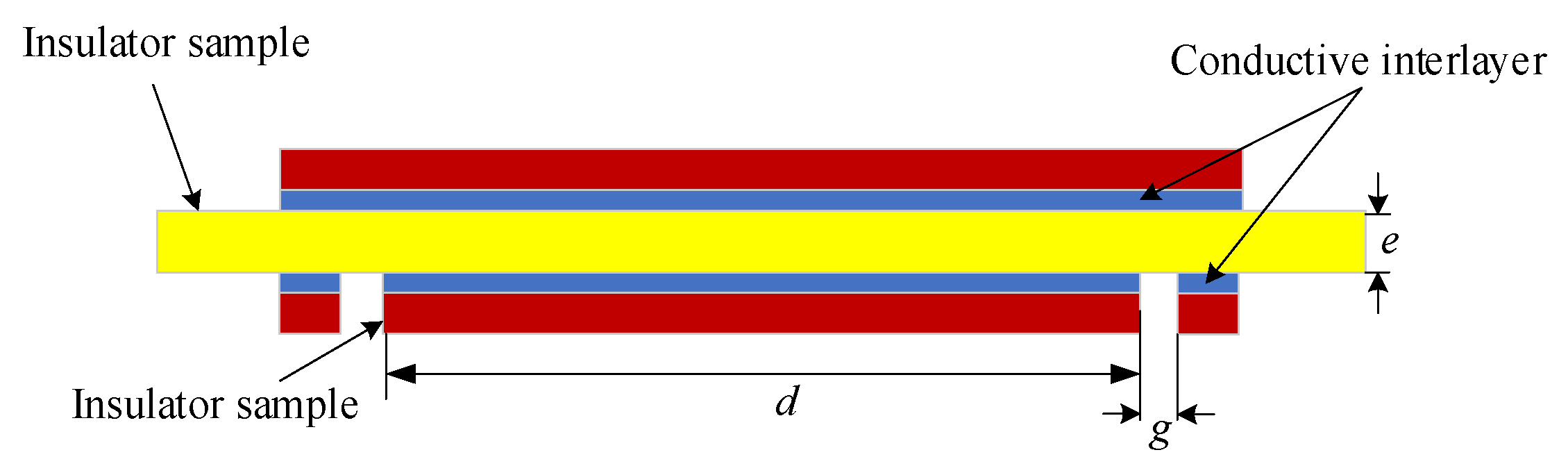
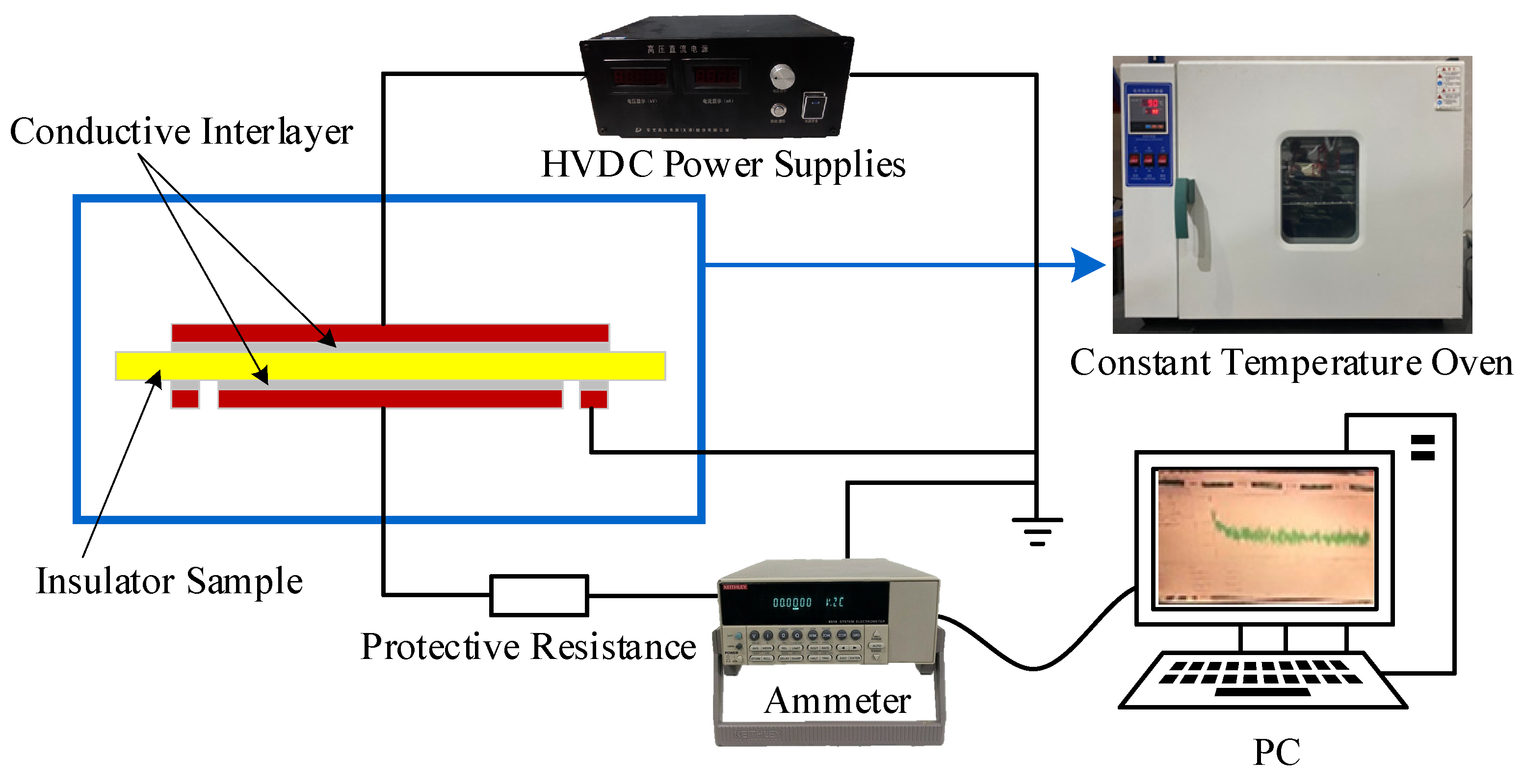
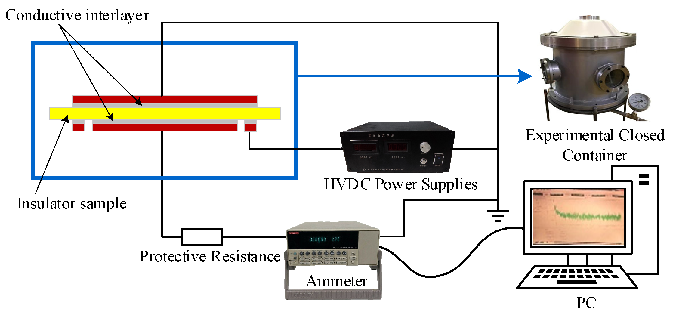
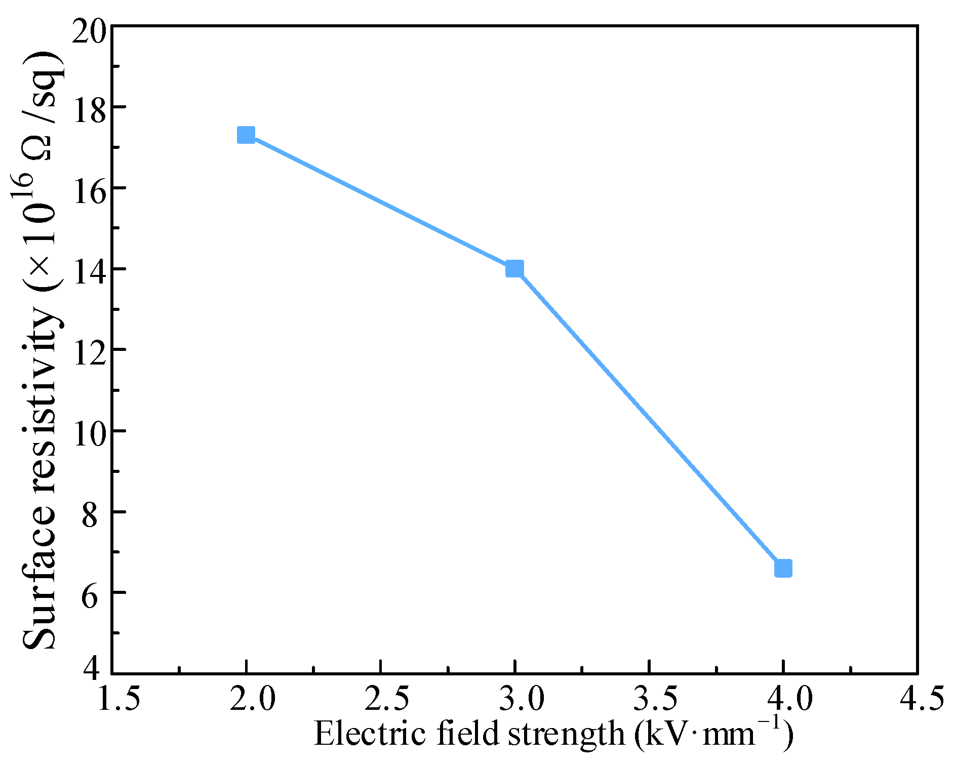
3. Insulator Conductivity Measurement

We designed and constructed a platform for measuring insulator bulk and surface conductivity parameters. We conducted the experiments using the three-electrode method, configuring the electrodes to conform to the IEC 60093 standard [33]. We performed current measurements using a Keithley Model 6485 Picoammeter (Keithley, Solon, OH, USA) with a 10 fA resolution, ensuring high precision. To verify repeatability, we conducted each conductivity measurement three times on five identical samples, achieving a relative error below 5%. The test samples were circular epoxy composite specimens with a thickness of 1 mm and a diameter of 120 mm, possessing material compositions identical to those of the insulator investigated in this study. Prior to testing, we cleaned all samples with anhydrous ethanol to remove surface contaminants, then dried the samples in a vacuum oven at 90 °C for 48 h to eliminate moisture. We positioned soft conductive rubber (the soft conductive rubber is a commercial product) between the electrodes and samples to ensure optimal electrical contact. The protective resistor of the experimental circuit is 1000 Ω. The rubber’s resistance is 2–3 Ω. Compared to the sample’s resistance of 1015 Ω, the conductive rubber’s impact is minimal, validating the measurement integrity.
To measure stable DC conduction currents and mitigate polarization effects, we extended the measurement duration, particularly under dry conditions. We observed that currents stabilized after approximately 3000 s (50 min), with no further attenuation. We averaged the stable current values to reduce measurement noise, ensuring reliable conductivity calculations. After each experiment, we depolarized the samples by grounding both ends and measured discharge currents before subsequent tests. We confirmed depolarization completion when discharge currents approached 0 pA, allowing the next experiment to proceed.
The volume resistivity is derived from the conductive current measured within the sample volume, while the surface resistivity is obtained from the conductive current measured along the insulator surface. As depicted in Figure 2, the electrode configuration diagram illustrates the setup, and for circular samples, both the volume resistivity and surface resistivity are calculated using Equations (20) and (22).
ρ R v = U I V S e
S = d + g 2 4
Here, ρRv is the bulk resistivity, U is the applied voltage, Iv is the current through the insulator volume, e is the insulator thickness, and S is the effective area.
ρ R s = U I s P g
P = π d + g
Here, ρRs is the surface resistivity, Is is the current through the insulator surface, and P is the effective perimeter.
The bulk resistivity parameter measurement platform is depicted in Figure 3. Experiments were conducted under standard atmospheric pressure, with test electrodes positioned within a temperature-controlled oven. Four distinct temperature conditions, 20 °C, 40 °C, 60 °C, and 80 °C, were set to span the typical operating range of DC GIL insulators, corresponding to conductor heating from currents up to 3150 A. Three experimental voltage levels, −2 kV, −4 kV, and −6 kV, were selected to assess resistivity variations, with each set of experiments performed on the same sample to ensure data consistency.
The bulk resistivity under various temperature and electric field conditions was determined through final experiments, as illustrated in Figure 4. Under a constant electric field, the volume resistivity decreases as temperature rises. Moreover, at 80 °C, the influence of electric field strength on volume resistivity diminishes, as shown in the experimental data.
Based on experimental data of insulator volume conductivity under varying temperature and electric field conditions, a functional relationship for the volume resistivity with respect to temperature and electric field was derived. Furthermore, the volume conductivity of the insulator is expressed by Equation (24), and the results demonstrate that the volume conductivity exhibits exponential growth with increasing temperature and electric field strength.
σ v = 1 ρ R v = 1 7.894 × 10 21 e 0.0476 T 0.139 E
The surface resistivity parameter measurement platform is illustrated in Figure 5, where the experimental electrodes are situated within a closed experimental container filled with SF6 gas at a pressure of 0.5 MPa.
Buret et al. [26] experimentally investigated the effects of temperature and electric field on the surface conductivity of insulators. The results show that, within a temperature range of 40 °C to 80 °C, the surface conductivity is more significantly influenced by the tangential electric field than by temperature. In this investigation, surface conductivity measurements were conducted under varying tangential electric field intensities at a constant ambient temperature of 20 °C. This is mainly because, within the temperature range examined in this study, the surface conductivity is primarily determined by changes in the tangential electric field, so the effects of temperature changes can be ignored while also taking into account the environmental conditions of the laboratory.
The surface resistivity distribution across varying electric field conditions at a constant temperature of 20 °C was determined through experimental measurements, as illustrated in Figure 6. Moreover, the surface resistivity declines with increasing electric field strength.
Analysis of the experimental data yielded a functional relationship describing the relationship between the surface resistivity of the insulator and the tangential electric field, while the surface conductance of the insulator can be expressed as
σ s = 1 ρ R s = 1 4.983 × 10 17 e 0.4818 E t
where Et is the tangential electric field strength, V/m.
We acknowledge that measuring surface conductivity at a fixed 20 °C may limit the generalizability of our findings, as temperature significantly affects conductivity. Future studies will explore surface conductivity across a broader temperature range to validate our conclusions under varied operational conditions.

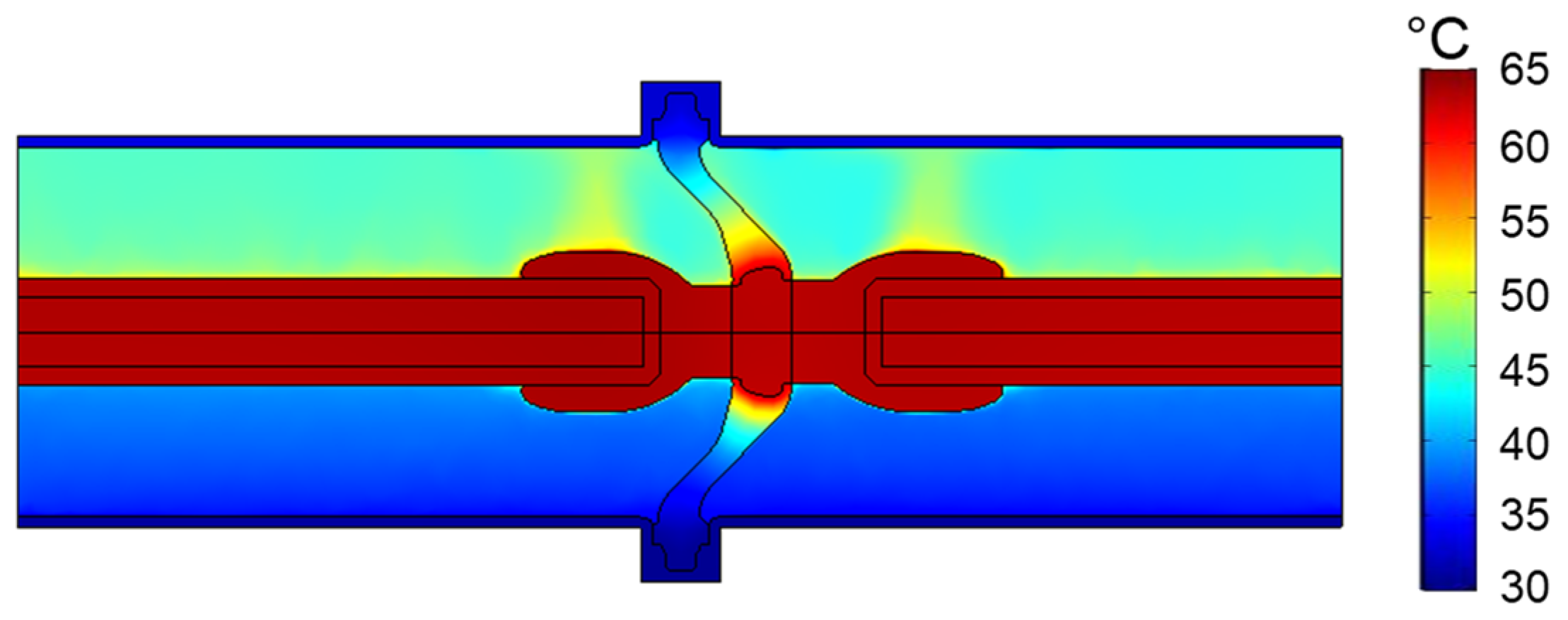
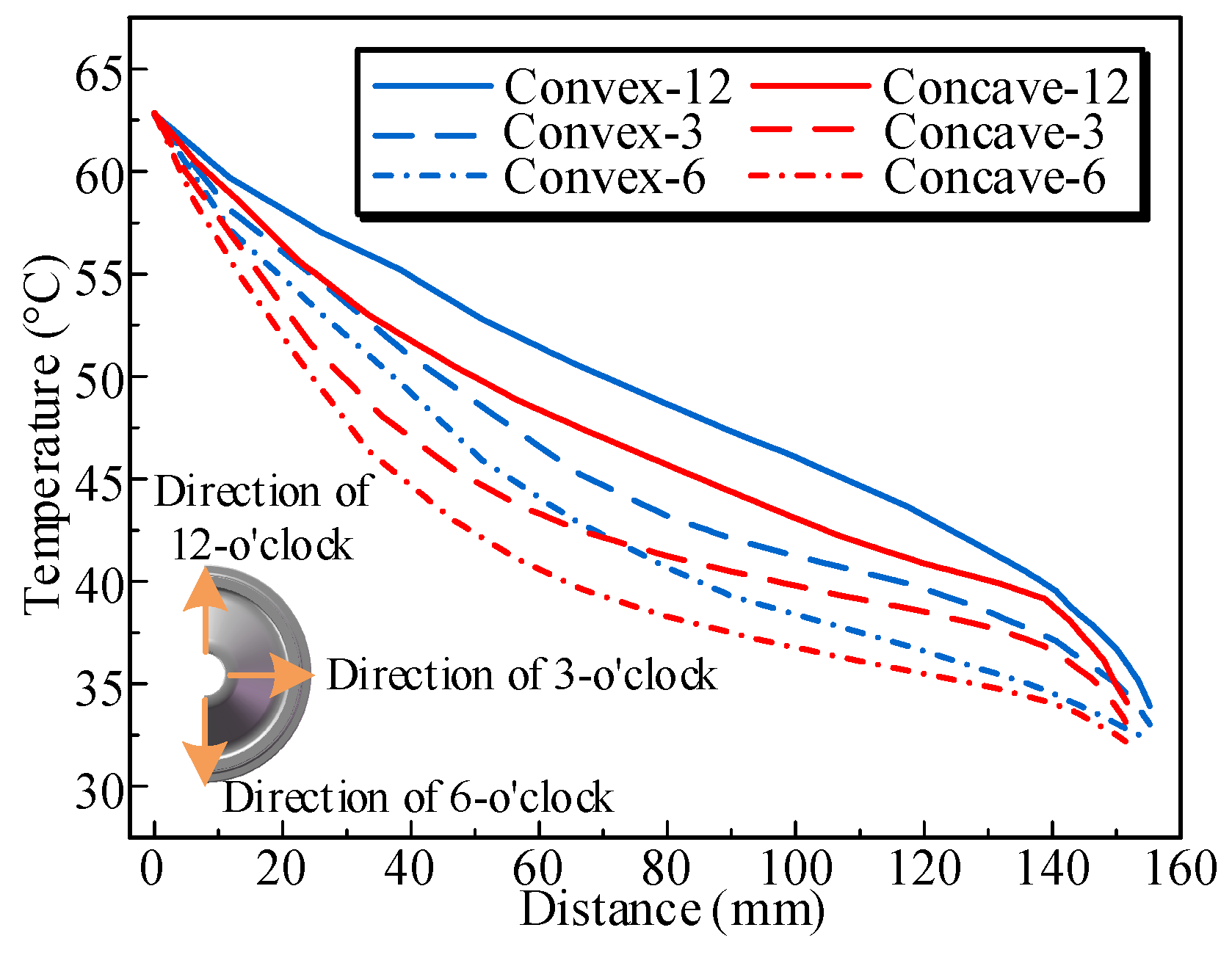
4. Insulator Temperature Distribution

Figure 7, which depicts finite element simulation (FEM) results, illustrates the temperature distribution of the DC GIL, showing a gradual decrease from the central conductor to the enclosure under operational conditions. We recorded a maximum temperature of 63.8 °C at the central conductor and a minimum temperature of 30.4 °C at the enclosure. Under horizontal arrangement conditions, the GIL exhibited pronounced temperature stratification, with the upper section exhibiting significantly higher temperatures than the lower section. Furthermore, we observed a localized temperature increase in the SF6 gas region immediately above the shielding cover.
As shown in Figure 8, the temperature distribution on the convex and concave surfaces of the insulator exhibits a similar trend, with the high-temperature region predominantly concentrated around the central conductor. We measured the highest temperature around the conductor at approximately 62.8 °C and the lowest temperature around the grounded enclosure at approximately 32 °C. The temperature on the convex side was higher than that on the concave side, and this temperature distribution characteristic may be attributed to the uneven gas flow. Specifically, this phenomenon can be attributed to the larger space on the convex side, where the gas convection heat transfer is more effective, whereas the concave side is constrained by the insulator’s structure, creating a narrower heat transfer space and consequently resulting in reduced convection heat transfer efficiency.
Figure 9 illustrates the temperature distribution on the insulator surface for different radial directions (12 o’clock, 3 o’clock, and 6 o’clock). Notably, the temperature distributions of the convex and concave surfaces exhibit significant differences, with the convex surface consistently exhibiting a higher overall temperature. The temperature gradually decreases with increasing distance from the central conductor. The temperature gradient varies considerably in different radial directions; specifically, the 12 o’clock direction exhibits a relatively gradual decrease in temperature, indicating a more homogeneous temperature distribution in this region. In contrast, the temperature fluctuations in the 3 o’clock and 6 o’clock directions are more pronounced, especially in the concave area, where a significant temperature gradient was observed. On the high-voltage side, due to conductor heating, the highest temperature recorded was 62.8 °C. Conversely, the lowest temperature at the grounded side varied with the radial direction. Additionally, in the intermediate region, the temperature difference between the convex and concave surfaces in the same direction was significant, a phenomenon attributable to convection heat transfer effects.

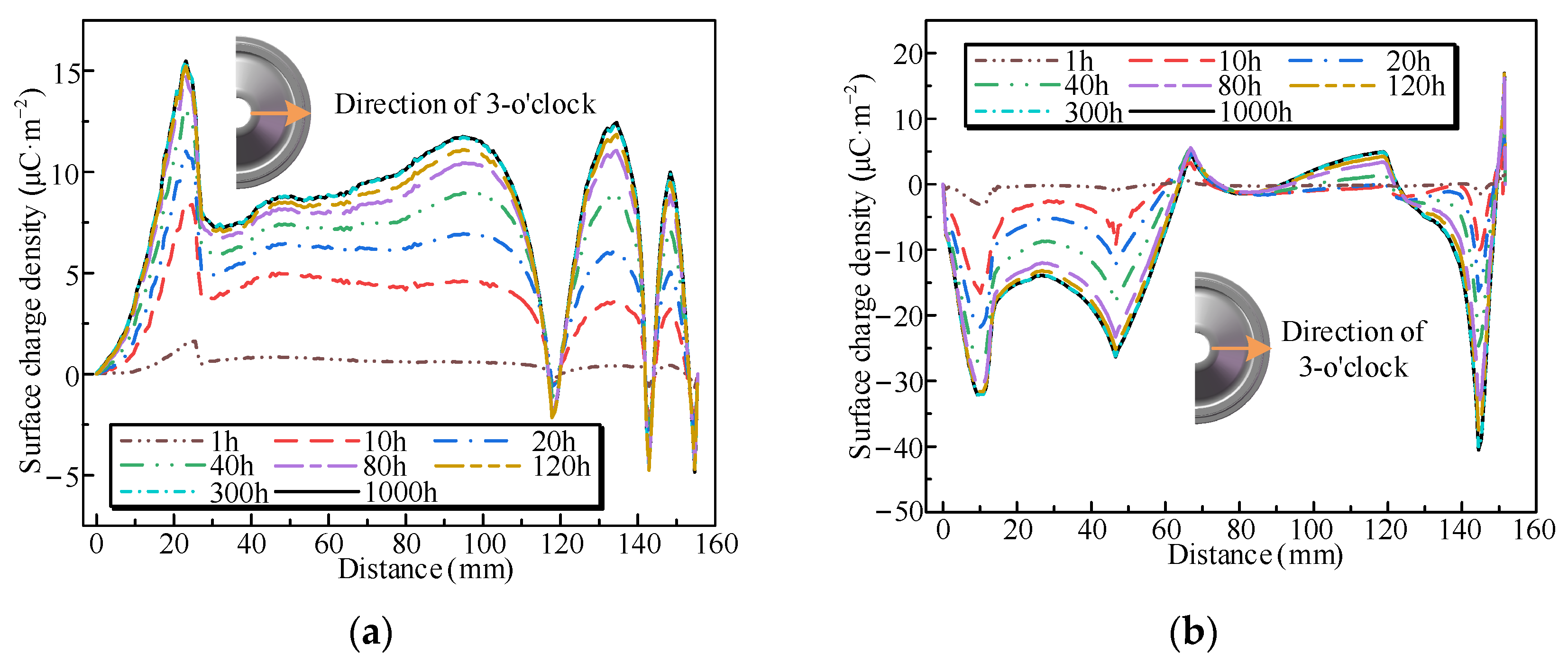
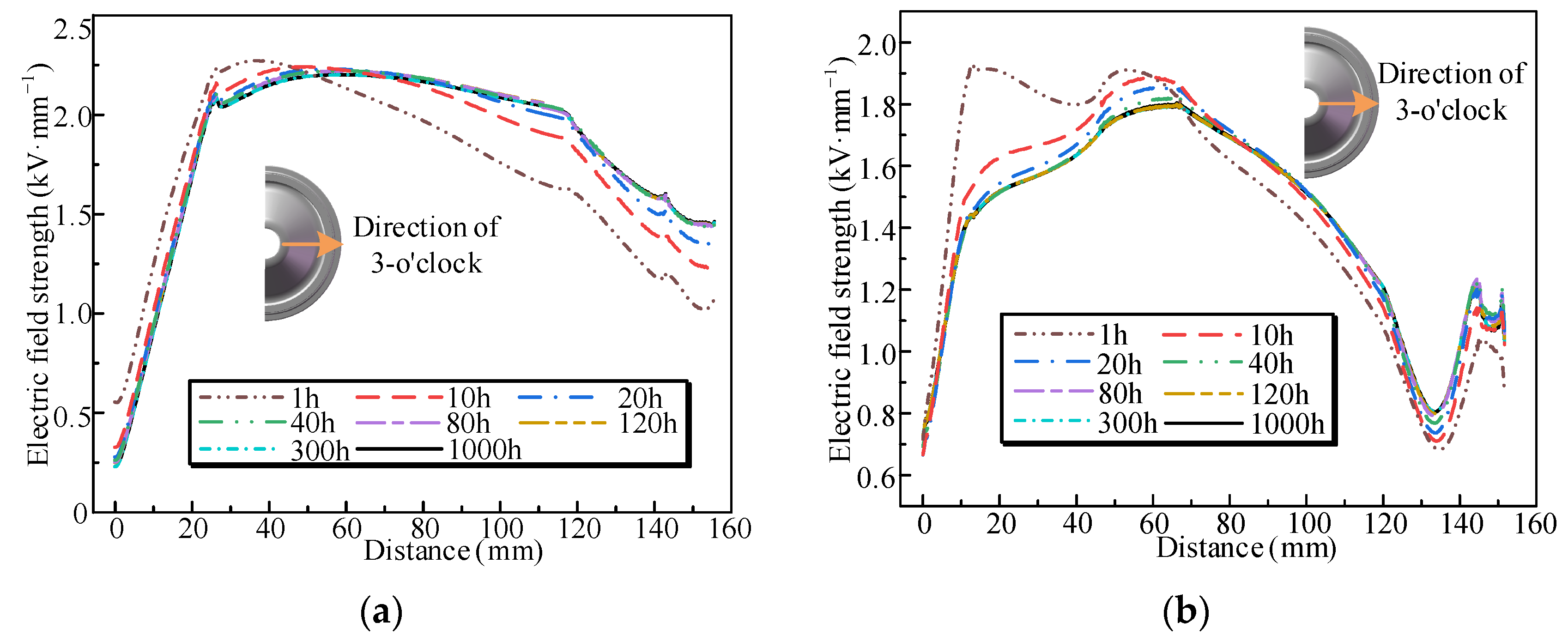
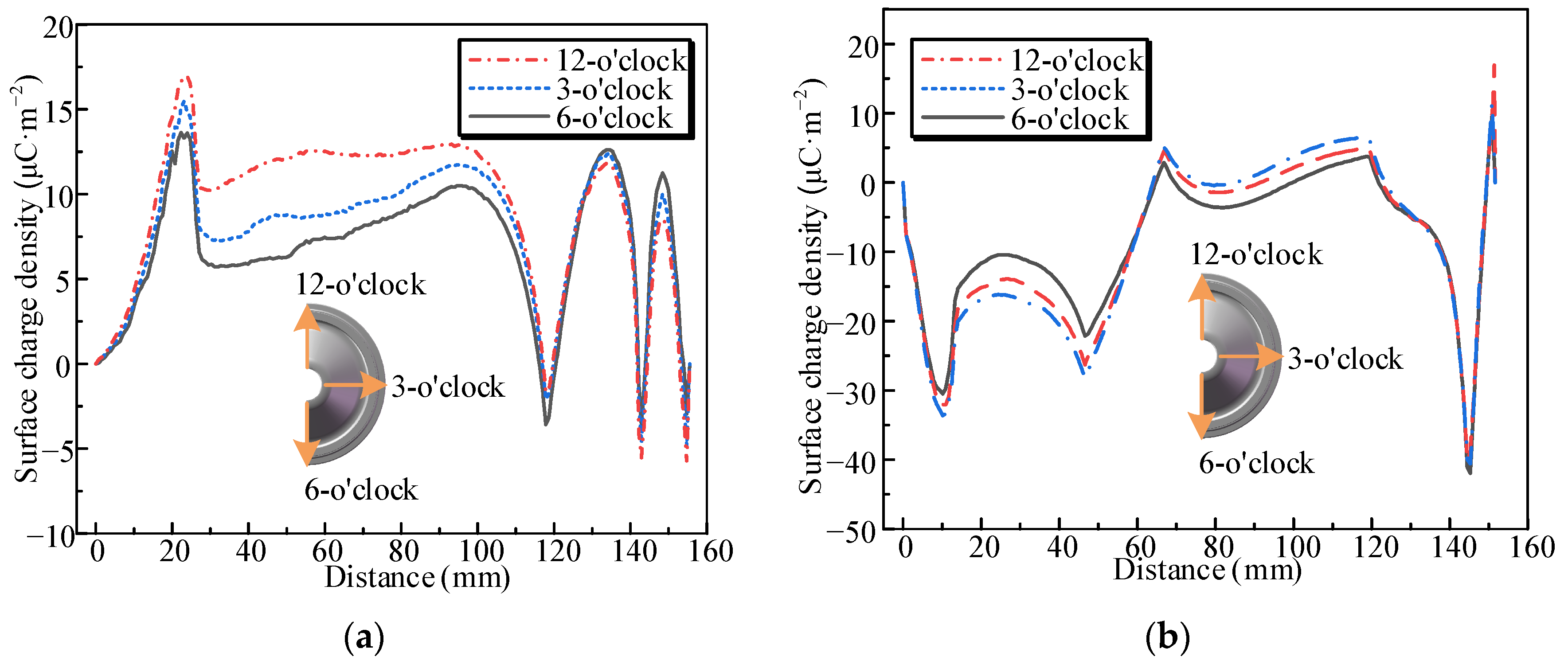
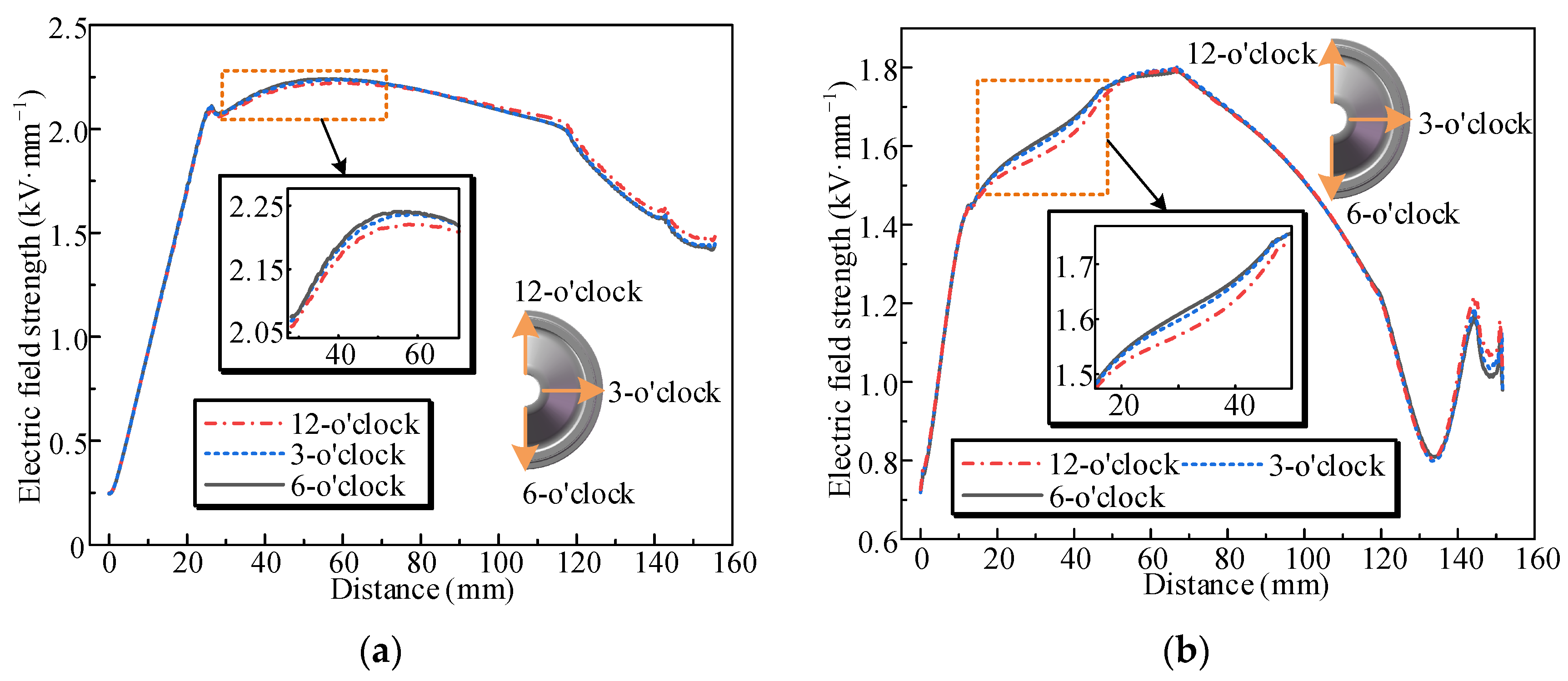
5. Insulator Surface Charge and Electric Field Distribution Under DC Voltage

The electric field distribution and the flow of electric field lines within the DC GIL are depicted in Figure 10, which presents the results of finite element simulation (FEM). Under positive-polarity DC voltage, the electric field lines flow out of the high-voltage side and into the low-voltage side, resulting in the aggregation of positive ions on the grounded side and negative ions on the high-voltage side. We observed that the electric field strength on the insulator’s convex surface significantly exceeds that on the concave surface. The electric field lines on the convex surface were dominated by outflow from the insulator, whereas those on the concave surface were dominated by inflow into the insulator. Consequently, negative ions in the SF6 gas region gather near the convex side, whereas positive ions gather near the concave side.
In DC GIL, the primary sources of surface charges on insulators can be categorized into three types: conduction from the SF6 gas side, conduction through the insulator bulk, and conduction along the insulator surface [16]. The distribution characteristics of surface charges are governed by the electric-field-driven carrier migration process. The charge behavior on the SF6 gas side is described by the particle dynamics Equations (9) and (10), where the gas-side current arises from the drift motion of positive and negative ions under Coulomb forces. Conduction through the insulator bulk and along its surface is characterized in this study by bulk conductivity and surface conductivity, as expressed in Equation (17).
Under DC voltage, the electric field within the GIL transitions from a capacitive to a resistive state, a process that essentially reflects the gradual saturation of charge accumulation within the field domain. The accumulation of surface charges on the insulator results from the interplay and eventual equilibrium among the three conduction mechanisms. This interplay is governed by Equation (17), which also elucidates the mechanism of surface charge accumulation. The polarity of surface charges primarily depends on the direction of the normal component of the electric field lines at the insulator surface, as illustrated in Figure 10. Under DC voltage, charges from both the solid (insulator) and gas sides migrate along the electric field direction, ultimately accumulating at the gas–solid interface. These charges may also transfer along the insulator surface under the influence of the tangential electric field, affecting the electric field distribution along the insulator surface until surface charge accumulation reaches equilibrium. When this equilibrium is achieved (at ∂ρ/∂t = 0), the capacitive electric field fully transitions to a stable resistive electric field distribution.
Under the application of DC voltage, the GIL electric field distribution gradually transitions from a capacitive field in the initial stage to a resistive field after stabilization [20], during which the evolution of the insulator surface charge density adheres to (17). Figure 11 illustrates the transient characteristics of the surface charge density distribution at the 3 o’clock direction of the insulator. We found that the convex surface predominantly accumulates positive charge, which increases gradually over time, indicating that ∂ρ/∂t in Equation (17) exceeds zero, with solid-side conduction dominating. Conversely, on the concave side of the insulator, the negative charge around the conductor and the enclosure gradually increases, while the negative charge in the middle region progressively decreases while the positive charge gradually increases. When the surface charge density decreases with time, it indicates that the parameter ∂ρ/∂t is less than 0, a condition where surface conduction dominates. As observed in Figure 11, during the first 40 h, the charge density on the convex and concave surfaces of the insulator fluctuates significantly, indicating an unstable initial charge distribution. Subsequently, the rate of change in surface charge density gradually decreases and stabilizes after approximately 300 h, indicating that the charge accumulation has reached an equilibrium state.
The time-varying characteristics of the surface charge density at different locations on the insulator surface (points A, B, and C) are illustrated in Figure 12. We observed that surface charge density at various locations increases gradually over time, with rapid changes during the initial stage. Subsequently, with time, all curves gradually approach stability, indicating that the charge density stabilizes after prolonged accumulation. Temperature significantly influences the charge accumulation process. Locations with higher temperatures (e.g., points A and B) exhibit a faster charge accumulation rate, whereas locations with lower temperatures (e.g., point C) demonstrate a relatively gradual accumulation process. The surface charge density at these locations stabilizes after approximately 300 h.
Figure 13 illustrates the transient distribution characteristics of the electric field along the insulator surface in the 3 o’clock direction. During the initial 40 h, the electric field exhibits significant variations along the surface of the insulator, particularly on the convex surface. This indicates that the electric field is significantly influenced by the accumulation of surface charges and the distribution of temperature during the initial stage. Subsequently, the variation of the electric field on the convex and concave surfaces gradually decreases. After 300 h, the electric field distribution stabilizes, indicating that the surface charge accumulation approaches equilibrium.
Figure 14 illustrates the characteristics of surface charge distribution along various radial directions after 300 h of DC voltage application. The charge distribution exhibits notable variations along different radial directions on both the convex and concave surfaces of the insulator, particularly in the middle region of the insulator surface. This phenomenon is primarily attributed to temperature variations along different radial directions of the insulator surface, which result in differences in the conductivity properties of the insulator.
Figure 15 illustrates the electric field distribution along different radial directions of the insulator surface. When charge accumulation reaches equilibrium, the electric field distribution varies in different radial directions, with the most pronounced differences observed in the 12 o’clock direction. This phenomenon is primarily attributed to the higher temperature observed in the 12 o’clock direction. Comparative analysis with the surface charge distribution characteristics presented in Figure 11 reveals a direct correlation: the magnitude of variation in charge distribution across different radial directions corresponds proportionally to the magnitude of variation in the electric field. This relationship confirms the direct influence of surface charge on the electric field distribution along the insulator surface [34].

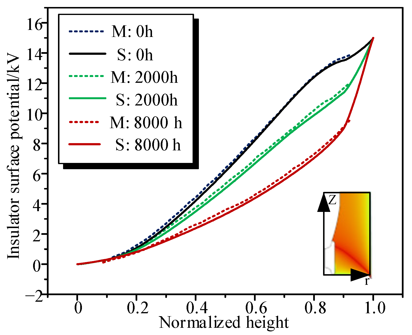
6. Insulator Surface Charge and Electric Field Distribution Under Polarity-Reversal Voltages

6.1. Polarity-Reversal Voltage Waveform

We present the polarity-reversal voltage waveform in Figure 16, where +U represents the preloading voltage and −U represents the reversal voltage. In this study, the preloading voltage is +200 kV. t2 moment corresponds to when the surface charge and electric field distribution along the surface have reached a stable state after 1000 h of voltage application, which also marks the initiation of polarity reversal. Time point t3 indicates when the voltage crosses the zero point, occurring 30 s into the polarity-reversal process. Time point t4 denotes when the voltage reaches the negative polarity working voltage. The polarity-reversal time, defined as the duration for voltage transition from +U to −U, is t4t2 = 60 s. Finally, time point t5 represents the state 1000 h after completion of the voltage reversal.

6.2. Insulator Surface Charge and Electric Field

The variation in charge density on the insulator surface during voltage polarity reversal is shown in Figure 17. The charge density distribution on the convex and concave surfaces of the insulator reaches a stable state after 1000 h of pre-pressurization. During the polarity-reversal process, the voltage decreases from the positive working voltage to zero and then increases to the negative working voltage in the reverse direction, whereas the charge accumulated on the insulator surface cannot be readily dissipated in a short time period.
Consequently, at the moment t4 after the polarity reversal is completed, residual charge remains on the insulator surface. By moment t5 following reversal, the residual surface charge has dissipated and the system has again reached a stable state, with surface charge distribution exhibiting opposite polarity compared to the pre-reversal state.
We show the transient characteristics of the electric field distribution along the insulator surface during voltage polarity reversal in Figure 18. In the t2t3 stage, the electric field strengths at the convex and concave surfaces of the insulator decrease gradually as the applied voltage decreases. At t3, when the voltage applied to the central conductor is 0, the surface electric field reaches its minimum value, which is generated by the residual charge present prior to reversal. In the t3t4 stage, the surface electric field gradually increases with the increasing negative polarity voltage. At t4, the residual charge present prior to polarity reversal causes significant distortion in the surface electric field distribution. Specifically, the maximum electric field at the convex surface increases by 13.6% compared to its pre-reversal value, while at the concave surface, it increases by approximately 47.2%, indicating that the degree of electric field distortion is significantly higher on the concave surface than on the convex surface. When the surface charge accumulation reaches a new steady state, the electric field distribution along the insulator surface becomes identical to that observed prior to polarity reversal.

7. Discussion

Surface charge accumulation on DC insulators has been extensively studied, yet experimental measurements remain challenging due to the need for high-voltage, high-current systems capable of sustaining coupled electrothermal fields over prolonged operation. Measuring transient charge distributions, particularly under polarity-reversal conditions, presents significant technical obstacles. As a result, short-term laboratory experiments to characterize transient surface charge distributions under electrothermal coupling are currently impractical. To address this, we experimentally measured the bulk and surface conductivity of insulators under conditions representative of practical engineering applications. These measurements enabled accurate simulations of surface charge accumulation and electric field distribution along the surface of DC GIL insulators under electrothermal coupling.
To validate our simulation model, we referenced experimental data from [17], which investigated transient electric field distributions in a gas–solid insulation system under DC voltage, measuring surface potential distributions on a post insulator at 0 h, 2000 h, and 8000 h. Using the geometric model and parameters from [17], we computed the surface potential distributions of a cylindrical insulator at the same time intervals under a 15 kV DC voltage. The simulated results, compared with experimental data from [17], are presented in Figure 19, where M denotes the experimental data from [17] and S represents the simulation results. The close agreement between them supports the validity of our model. Future work will focus on developing advanced experimental measurement systems and refining measurement techniques to overcome current limitations and enable direct characterization of transient charge distributions under electrothermal coupling.

8. Conclusions

In this paper, the characteristics of charge accumulation and electric field distribution on the surface of a ±200 kV DC GIL basin-type insulator was investigated under multi-physical field coupling conditions. The main conclusions of this study are as follows:
(1)
The insulator bulk conductivity and surface conductivity parameters under different temperature and electric field conditions were determined experimentally, from which the corresponding fitting equations were established. The insulator bulk conductivity increases exponentially with increasing temperature and electric field, whereas the surface conductivity increases exponentially with increasing tangential electric field.
(2)
When the DC GIL operates at a current of 3150 A, the temperature of the central conductor reaches a maximum of approximately 63.8 °C, while the enclosure’s temperature remains at a minimum of about 30.4 °C. The maximum temperature of the insulator near the conductor is approximately 62.8 °C, in contrast to the minimum insulator temperature recorded near the enclosure, which is around 32 °C. Notably, convex surface temperatures consistently exceed those of concave surfaces, with significant thermal variations observed across different radial orientations (12 o’clock, 3 o’clock, and 6 o’clock).
(3)
Under DC voltage, the electric field distribution gradually transitions from a capacitive field to a resistive field. On the insulator’s convex surface, positive charges progressively accumulate, while negative charges increase on the concave surface. The surface charge accumulation is more rapid in the high-temperature regions of the insulator. The surface charge and electric field exhibit significant changes within the first 40 h. After 300 h, surface charge accumulation approaches equilibrium, and the electric field stabilizes. Following stabilization, the difference in surface charge across different radial directions is substantial, whereas the difference in the electric field remains relatively small.
(4)
When voltage polarity reversal occurs, the charges accumulated on the insulator surface cannot be fully dissipated within a short time frame. This residual charge after the reversal significantly distorts the electric field along the surface, resulting in an increase of 13.6% in maximum field strength on the convex surface and 47.2% on the concave surface. Notably, the concave surface exhibits the most severe distortion of the electric field following polarity reversal.

Author Contributions

Conceptualization, J.J. and X.L.; methodology, J.J. and Z.G.; software, J.J.; validation, J.J. and Z.G.; formal analysis, J.J. and X.L.; investigation, J.J. and Z.G.; resources, J.X.; data curation, J.J.; writing—original draft preparation, J.J.; writing—review and editing, J.J.; visualization, J.J. and Z.G.; supervision, X.L.; project administration, J.X.; funding acquisition, J.X. All authors have read and agreed to the published version of the manuscript.

Funding

This research was funded by the Basic Research Special Project of Natural Science Foundation of Shenyang, China (24-202-6-02).

Institutional Review Board Statement

Not applicable.

Informed Consent Statement

Not applicable.

Data Availability Statement

The original contributions presented in this study are included in the article. Further inquiries can be directed to the corresponding author.

Acknowledgments

This paper has received support from the Institute of High Voltage and Power Systems at Shenyang University of Technology. The author extends gratitude to Jianyuan Xu. In addition, the author sincerely thanks Xin Lin.

Conflicts of Interest

The authors declare no conflicts of interest.

References

  1. Koch, H.J. Gas Insulated Transmission Lines (GIL); John Wiley & Sons: London, UK, 2011; pp. 4–6. [Google Scholar]
  2. Magier, T.; Tenzer, M.; Koch, H. Direct Current Gas-Insulated Transmission Lines. IEEE Trans. Power Deliv. 2018, 33, 440–446. [Google Scholar] [CrossRef]
  3. Wang, X.; Zhu, Y.; Wang, C.; Wu, K.; Tu, D. Effect of Space Charge on Electric Field Distribution at the Insulating Interface Between DC Cable and Accessory. High Volt. Eng. 2015, 41, 2681–2688. [Google Scholar] [CrossRef]
  4. Li, C.; Lin, C.; Zhang, B.; Li, Q.; Liu, W.; Hu, J.; He, J. Understanding Surface Charge Accumulation and Surface Flashover on Spacers in Compressed Gas Insulation. IEEE Trans. Dielectr. Electr. Insul. 2018, 25, 1152–1166. [Google Scholar] [CrossRef]
  5. Li, Q.; Naderiallaf, H.; Lei, Z.; Wang, Y.; Liu, P.; Zhang, L.; Wang, Z.; Zhang, Z. Surface Charge Pattern Analysis Based on the Field-Dependent Charging Theory: A Review. IEEE Trans. Dielectr. Electr. Insul. 2020, 27, 257–269. [Google Scholar] [CrossRef]
  6. Zhou, H.; Ma, G.; Wang, C.; Wang, J.; Zhang, G.; Tu, Y.; Li, C. Review of Charge Accumulation on Spacer of Gas Insulated Equipment at DC Stress. CSEE J. Power Energy Syst. 2019, 6, 496–517. [Google Scholar] [CrossRef]
  7. Qiao, Y.J.; Liang, R.; Gao, P.; Zhu, S.Y.; Chen, C.Y.; Qin, Y.X.; Tang, X.Z. Heat Transfer Analysis of Different Conditions for SF6/N2 Gas-Insulated Transmission Lines. IEEE Trans. Power Deliv. 2021, 36, 831–840. [Google Scholar] [CrossRef]
  8. Zhou, H.; Ma, G.; Li, C.; Shi, C.; Qin, S. Impact of Temperature on Surface Charges Accumulation on Insulators in SF6-Filled DC-GIL. IEEE Trans. Dielectr. Electr. Insul. 2017, 24, 601–610. [Google Scholar] [CrossRef]
  9. Li, C.; Zhang, C.; Lv, J.; Liang, F.; Liang, Z.; Fan, X.; Riechert, U.; Li, Z.; Liu, P.; Xue, J.; et al. China’s 10-Year Progress in DC Gas-Insulated Equipment: From Basic Research to Industry Perspective. iEnergy 2022, 1, 400–433. [Google Scholar] [CrossRef]
  10. Qi, B.; Gao, C.; Li, C.; Xiong, J. The Influence of Surface Charge Accumulation on Flashover Voltage of GIS/GIL Basin Insulator under Various Voltage Stresses. Int. J. Electr. Power Energy Syst. 2019, 105, 514–520. [Google Scholar] [CrossRef]
  11. Du, B.; Dong, J.; Liang, H.; Kong, X. Polarity Reversal and Over Voltage Affecting Discharge Inception of Tri-Post Insulator in ±800 kV GIL. IEEE Trans. Dielectr. Electr. Insul. 2022, 29, 223–230. [Google Scholar] [CrossRef]
  12. Zhang, B.; Gao, W.; Hou, Y.; Zhang, G. Surface Charge Accumulation and Suppression on Fullerene-Filled Epoxy-Resin Insulator under DC Voltage. IEEE Trans. Dielectr. Electr. Insul. 2018, 25, 2011–2019. [Google Scholar] [CrossRef]
  13. Luo, Y.; Tang, J.; Pan, Z.; Pan, C. How Temperature and Pressure Affect the Electric Field Distribution in HVDC GIS/GIL: A Numerical Study. IEEE Trans. Dielectr. Electr. Insul. 2021, 28, 1334–1342. [Google Scholar] [CrossRef]
  14. Zhang, L.; Tang, D.; Yu, D.; Zhang, Z. Temperature-Dependent Surface Charge Accumulation for Vertical and Horizontal HVDC GIL. IEEE Trans. Dielectr. Electr. Insul. 2023, 30, 1868–1876. [Google Scholar] [CrossRef]
  15. Zhang, B.; Qi, Z.; Zhang, G. Thermal Gradient Effects on Surface Charge of HVDC Spacer in Gas Insulated System. In Proceedings of the 2016 IEEE Conference on Electrical Insulation and Dielectric Phenomena (CEIDP), Toronto, ON, Canada, 16–19 October 2016; pp. 703–706. [Google Scholar]
  16. Schueller, M. Role and Impact of Different Charge Sources on Surface Charge Accumulation in Gas Insulated HVDC Systems. Ph.D. Thesis, University of Eastern Switzerland OST, Rapperswil-Jona, Switzerland, 2014. [Google Scholar]
  17. Winter, A.; Kindersberger, J. Transient Field Distribution in Gas-Solid Insulation Systems under DC Voltages. IEEE Trans. Dielectr. Electr. Insul. 2014, 21, 116–128. [Google Scholar] [CrossRef]
  18. Winter, A.; Kindersberger, J. Stationary Resistive Field Distribution along Epoxy Resin Insulators in Air under DC Voltage. IEEE Trans. Dielectr. Electr. Insul. 2012, 19, 1732–1739. [Google Scholar] [CrossRef]
  19. Ma, G.; Zhou, H.; Lu, S.-J.; Wang, Y.; Liu, S.; Li, C.; Tu, Y.-P. Effect of Material Volume Conductivity on Surface Charges Accumulation on Spacers under Dc Electro-Thermal Coupling Stress. IEEE Trans. Dielectr. Electr. Insul. 2018, 25, 1211–1220. [Google Scholar] [CrossRef]
  20. Luo, Y.; Tang, J.; Pan, C.; Pan, Z.; Li, Y.; Cui, Z. Dynamics of Surface Charge and Electric Field Distributions on Basin-type Insulator in GIS/GIL Due to Voltage Polarity Reversal. High Volt. 2020, 5, 151–159. [Google Scholar] [CrossRef]
  21. Yan, W.; Li, C.; Lei, Z.; Han, T.; Zhang, Z.; Fabiani, D. Surface Charging on HVDC Spacers Considering Time-Varying Effect of Temperature and Electric Fields. IEEE Trans. Dielectr. Electr. Insul. 2019, 26, 1316–1324. [Google Scholar] [CrossRef]
  22. Li, X.; Wan, M.; Zhang, G.; Lin, X. Surface Charge Characteristics of DC-GIL Insulator Under Multiphysics Fields: 3-D Modeling. IEEE Trans. Dielectr. Electr. Insul. 2022, 29, 1608–1616. [Google Scholar] [CrossRef]
  23. Li, X.; Wan, M.; Zhang, G.; Lin, X. Surface Charge Characteristics of DC-GIL Insulator Under Multiphysics Coupled Field: Effects of Ambient Temperature, Load Current, and Gas Pressure. IEEE Trans. Dielectr. Electr. Insul. 2022, 29, 1530–1539. [Google Scholar] [CrossRef]
  24. Zheng, Z.; Li, Z.; Wu, Y.; Wang, H.; Du, B. The Evolution of Space Charge and Electric Field in HVDC Cable under Polarity Reversal Voltage Superimposed with Temperature Gradient. In Proceedings of the 2024 IEEE 5th International Conference on Dielectrics (ICD), Toulouse, France, 30 June–4 July 2024; pp. 1–4. [Google Scholar]
  25. Chen, J.; Xue, J.; Dong, J.; Li, Y.; Deng, J.; Zhang, G.-J. Effects of Surface Conductivity on Surface Charging Behavior of DC-GIL Spacers. IEEE Trans. Dielectr. Electr. Insul. 2020, 27, 1038–1045. [Google Scholar] [CrossRef]
  26. Zavattoni, L. Conduction Phenomena Through Gas and Insulating Solids in HVDC Gas Insulated Substations, and Consequences on Electric Field Distribution. Ph.D. Thesis, Université de Grenoble, Grenoble, France, 2014. [Google Scholar]
  27. Wu, X.; Shu, N.; LI, H.; LI, L. Temperature Rise Numerical Calculation and Correlative Factors Analysis of Gas-Insulated Transmission Lines. Trans. China Electrotech. Soc. 2013, 28, 65–72. [Google Scholar] [CrossRef]
  28. Wu, G.; Yao, L.; Peng, R. Handbook of Aluminum and Aluminum Alloy Materials; Science Press: Beijing, China, 1994; pp. 233–236. [Google Scholar]
  29. Kindersberger, J.; Wiegart, N.; Boggs, S.A. Ion Production Rates in SF6 and the Relevance Thereof to Gas-Insulated Switchgear. In Proceedings of the Conference on Electrical Insulation & Dielectric Phenomena-Annual Report 1985, Amherst, NY, USA, 20–24 October 1985; pp. 123–129. [Google Scholar]
  30. Morrow, R. A Survey of the Electron and Ion Transport Properties of SF6. IEEE Trans. Plasma Sci. 1986, 14, 234–239. [Google Scholar] [CrossRef]
  31. Codina, R. Comparison of Some Finite Element Methods for Solving the Diffusion-Convection-Reaction Equation. Comput. Methods Appl. Mech. Eng. 1998, 156, 185–210. [Google Scholar] [CrossRef]
  32. Tran, T.N.; Golosnoy, I.O.; Lewin, P.L.; Georghiou, G.E. Numerical Modelling of Negative Discharges in Air with Experimental Validation. J. Phys. D Appl. Phys. 2011, 44, 015203. [Google Scholar] [CrossRef]
  33. IEC 60093:1980; Methods of Test for Volume Resistivity and Surface Resistivity of Solid Electrical Insulating Materials. IEC Webstore: Geneva, Switzerland, 1980.
  34. Jia, Z.; Zhang, B.; Fan, J.; Li, J.; Li, P.; Zhang, Q. Study of Charge Accumulation Along the Insulator Surface in the DC GIL. Proc. CSEE 2010, 30, 112–117. [Google Scholar] [CrossRef]
Figure 1. Geometric model of the ±200 kV DC GIL.
Applsci 15 07061 g001
Figure 2. Schematic diagram of the electrode device.
Applsci 15 07061 g002
Figure 3. Bulk resistivity measurement platform.
Applsci 15 07061 g003
Figure 4. Bulk resistivity measurement data.
Applsci 15 07061 g004
Figure 5. Surface conductivity measurement platform.
Applsci 15 07061 g005
Figure 6. Surface resistivity measurement data.
Applsci 15 07061 g006
Figure 7. DC GIL temperature distribution.
Applsci 15 07061 g007
Figure 8. Basin-type insulator temperature distribution.
Applsci 15 07061 g008
Figure 9. Temperature of insulator surface in different directions.
Applsci 15 07061 g009
Figure 10. Cloud map of electric field line distribution. (The yellow arrows indicate a local magnification, and the red arrows indicate the direction of the electric field lines.)
Applsci 15 07061 g010
Figure 11. Transient characteristics of surface charge density on basin-type insulators: (a) convex surface; (b) concave surface.
Applsci 15 07061 g011
Figure 12. Time-varying characteristics of surface charge density at different locations.
Applsci 15 07061 g012
Figure 13. Transient characteristics of surface electric field on basin-type insulators: (a) convex surface; (b) concave surface.
Applsci 15 07061 g013
Figure 14. Surface charge distribution along various radial directions: (a) convex surface; (b) concave surface.
Applsci 15 07061 g014
Figure 15. Surface electric field distribution along various radial directions: (a) convex surface; (b) concave surface.
Applsci 15 07061 g015
Figure 16. Polarity-reversal voltage waveform.
Applsci 15 07061 g016
Figure 17. Transient characterization of surface charge density at polarity-reversal voltages: (a) convex surface; (b) concave surface.
Applsci 15 07061 g017
Figure 18. Transient characterization of the electric field along the surface at a polarity reversal voltage: (a) convex surface; (b) concave surface.
Applsci 15 07061 g018
Figure 19. Comparison of simulation results with experimental data in the literature.
Applsci 15 07061 g019
Table 1. Center conductor and enclosure thermodynamic parameters.
Density kg/m3Specific Heat Capacity J/(kg·K)Thermal Conductivity W/(m·K)
Conductor2690895218
Enclosure2660819152
Table 2. Insulator thermodynamic parameters.
Temperature K301323.6348.8373.85398.7
Thermal Conductivity W/(m·K)0.9460.9670.9340.9170.984
Specific Heat Capacity J/(kg·K)0.8800.9491.0181.0751.195
Disclaimer/Publisher’s Note: The statements, opinions and data contained in all publications are solely those of the individual author(s) and contributor(s) and not of MDPI and/or the editor(s). MDPI and/or the editor(s) disclaim responsibility for any injury to people or property resulting from any ideas, methods, instructions or products referred to in the content.

