Article

A High-Conversion Ratio Multiphase Converter Realized with Generic Modular Cells

by
Eli Hamo
,
Michael Evzelman
and
Mor Mordechai Peretz
*
The Center for Power Electronics and Mixed-Signal IC, The School of Electrical and Computer Engineering, Ben-Gurion University of the Negev, Beer-Sheva 8410501, Israel
*
Author to whom correspondence should be addressed.
Appl. Sci. 2025, 15(12), 6818; https://doi.org/10.3390/app15126818
Submission received: 9 April 2025 / Revised: 8 June 2025 / Accepted: 10 June 2025 / Published: 17 June 2025

Abstract

:
This paper introduces a high-conversion ratio multiphase nonisolated converter built from generic LC cells. The unique architecture that hinges on a generic capacitor inductor switching module enables the high modularity of the topology, providing a quick extension of the converter design in an interleaved configuration for lower ripple and higher current output. The generic module comprises the basic power components of a nonisolated DC–DC converter, where the unique interaction between the capacitor and the inductor results in a soft charging operation, which curbs the losses of the converter, and contributes to a higher efficiency. Additional features of the new converter include a significantly extended effective duty ratio, and a lower voltage stress on the switches, a very high output current, and architecture-inherent output current sharing that balances the loading between the phases. In addition, a power extension using a paralleling and interleaving approach is presented to provide higher output current capabilities. Simulation and experimental results of a modular interleaved three-phase prototype demonstrate an excellent proof of concept and agree well with the theoretical analyzes developed in this study.

1. Introduction

With the development of cloud computing and data centers, the demand for efficient, high-power conversion has significantly grown up [1,2,3,4,5]. In recent years, DC distribution systems have been widely used to replace the traditional AC systems in data centers due to their higher efficiency. The increased popularity of using a 48 V DC power distribution network in today’s computing industry, where multiple CPUs and DRAMs are part of the main consumer, has reinforced the need for DC–DC Point of Load (PoL) systems capable of carrying the conversion of 48 V-to-1.x V. The majority of modern supply methods are using either a two-stage conversion in series such as 48 V-to-12 V and then 12 V-to-1.x V [6,7,8,9,10,11,12,13,14,15], or a direct-conversion approach 48 to 1.x V that could be magnetically isolated or not [16,17,18,19,20,21,22,23,24,25,26,27,28,29,30,31,32,33,34].
Recently, step-down conversion solutions based on unregulated switched-capacitor converters (SCC) as a first stage, followed by an inductor based regulated stage, i.e., derivatives of buck converters, have been introduced [6,8,10,35]. Multiphase interleaved buck converters are generally used for the point of load stage [12,36,37], achieving fast dynamic response and delivering a high current to the load, while reducing the output filter volume and obtaining a high efficiency over wide load range. In a two-step high-conversion approach, the objective of the first-stage converter is to maintain a high efficiency and loosely hit the operation region of the second stage [16,17]. Even though the first and the second stages are efficient on their own, the overall conversion efficiency after both conversions is insufficient for many competitive applications, due to the multiplication of the two efficiencies. In addition, bulky transformers or heat sinks [10,24,25] are not desirable for applications that require both power density and large conversion ratios.
The development of GaN-based FETs enables the use of high-density single-stage conventional buck converters for the direct-conversion approach. Yet, applying a single-stage buck converter or using multilevel buck converters for the full 48 V-to-1.x V conversion remains impractical due to the time resolution challenges, associated with narrow “on” times and very high switching frequencies that require PWM generation hardware with precision on the order of ten picoseconds in both the duty cycle and jitter of the signal [31,38]. In addition, duty cycles on the order of 1/48 are still very challenging in terms of RMS losses in the circuit. Some prior art suggests using advanced control methods to improve the efficiency of the conventional buck converters [39,40,41,42,43,44,45,46]. Other solutions consist of combinations of the buck topology with flying capacitor topology, offering several advantages over the two-stage conversion solutions [12,21], such as extended conversion ratio, wide dynamic range, and the integration of multilevel and multiphase architecture features in a single conversion stage, which reduce inductor voltage swing and lower the switching loss. One derivative of the multiphase buck converter with extended-duty cycles—known as the series-capacitor buck converter—performs better than a buck converter and stands out as an attractive solution [23,26,27]. This converter can produce fast dynamic response to load changes, along with symmetrical operation and natural current sharing between phases, and reduce transistors’ voltage stress. However, previously documented topologies with extended-duty ratio are somewhat limited for application in high-power cases, where a very high conversion ratio and high currents are involved. One solution to higher voltage gain is presented in [34] using a three-phase series-capacitor buck converter. However, it lacks the current extension and architecture generalization. This work presents a full architecture analysis and generalization of a series-capacitor buck to higher orders, increasing both the conversion ratio and current output capabilities. In addition, this work covers advanced topics and analyzes those such as soft charging, boundary operation, voltage versus duty cycle evaluation, component stress analysis, and a modularization method using a generic cell.
From a design perspective, many power converters can be analyzed as being constructed around a fundamental cell [10,45,46,47]. This fundamental cell enables the implementation of several different topologies, which share a mode of operation and provide various conversion ratios by reconfiguring its connection orientation. For instance, common converter topologies such as buck, boost, and buck–boost share a core structure comprising a single inductor and two switches [48,49,50]. Despite utilizing the same basic components, these converters achieve different functionalities through distinct topological arrangements.
A power design methodology based on a fundamental cell provides numerous advantages, including modularity, which simplifies the design process and supports easy scalability. It promotes standardization, reducing design complexity while ensuring consistent performance across various applications. This approach enhances effectiveness by enabling component reuse, minimizes development time, and streamlines validation and testing efforts. Furthermore, it improves manufacturability by maintaining uniformity during fabrication and reduces costs through shared design and testing efforts, making it a highly effective strategy for power system development.
The objective of this study is to introduce a modular construction approach of a very-high conversion ratio multiphase converter, based on a generic, switched LC cell. The converter (Figure 1) is constructed from a chain of identical building blocks, each consisting of a switched inductor–capacitor pair that forms a stacked series-capacitor converter frontend whereas the backend of the converter is a set of parallel or interleaved inductors. This modular stacking of generic cells allows flexibility in the design, enabling high-power and high-conversion ratio without sacrificing the end-to-end efficiency of the converter, since the operation relies on single-cycle power processing from source to load, regardless of the number of modules stacked. Current sharing is maintained throughout the multiphase backend, allowing state-of-the-art performance in terms of power considerations and converter sizing for operation in both steady-state and transient modes.
The rest of the paper is organized as follows. Section 2 presents the operation principle and the construction methodology of modular stacking of identical switched inductor–capacitor cells. In Section 3, a full steady-state analysis of a three-level converter is delineated. The generalization of voltage and power stacking is analyzed in Section 4. Simulation and experimental results are provided in Section 5, and Section 6 concludes the paper.

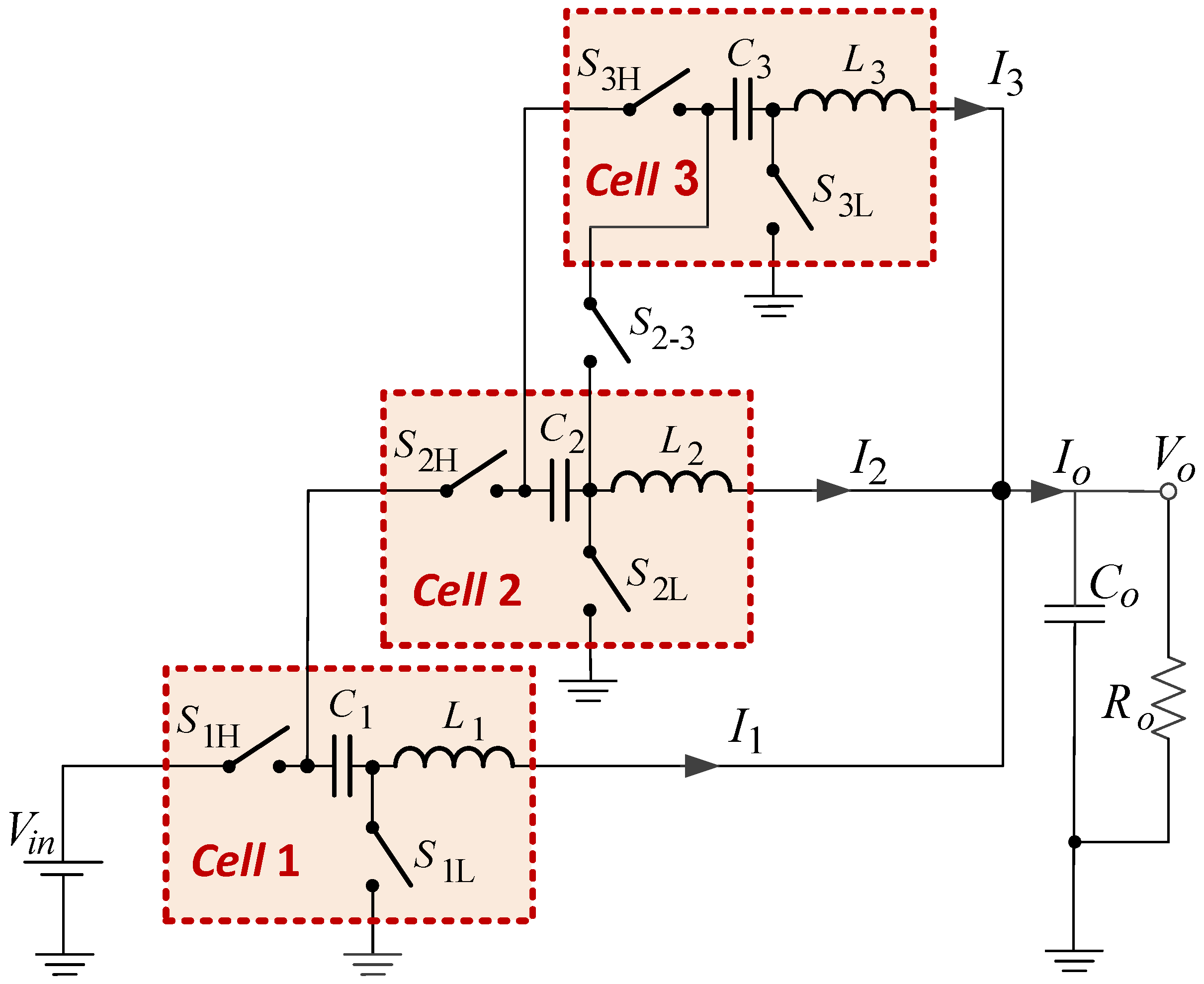
2. Modular Multiphase Step-Down Converter

The development of a generic cell as a basic building block is shown in Figure 2. The cell includes an inductor, a capacitor, and a pair of complementary switches. Multiple cells can be connected for increased energy processing. This unique approach of designing with a generic cell enables the extension of the converter to any number of phases, with the benefit of higher duty ratio resolution, lower voltage stress on the transistors, and inherent current balancing [51]. These benefits make the multiphase topology an ideal candidate for high output current and high conversion ratio applications. The combination of generic cells for the implementation of a high conversion ratio DC–DC converter is described and analyzed in the following sections. Throughout this paper, the concept is presented and analyzed on a configuration of three cells, namely, a three-phase buck converter, as illustrated in Figure 1. The main building block is a generic cell (Figure 2) comprised of an inductor, a capacitor, and two complementary switches. The cells connection follows a simple procedure. Port “a” of the cell (Figure 2) is connected to the previous cell (to Vin in the case of the first cell), port “b” of the cell is connected to the next cell, and port “c” is connected to the load. To complete the converter, one additional switch per converter (S2-3 in Figure 1) is added. It provides a discharge path for the last cell capacitor.
The operation of the proposed topology is described using the ideal timing diagram in Figure 3 and the sub-circuits with highlighted current paths in Figure 4. For simplicity, this analysis assumes that the voltage ripple across all capacitors is negligible compared to their DC levels. The switching period is divided into six intervals, corresponding to six states (I–VI). Odd-numbered intervals represent the charging phases for each cell, while even-numbered intervals correspond to balancing states. In this context, a “cell” refers to an individual building block, whereas a “phase” denotes the electrical components within a single cell that contributes to supplying the load current.
As in typical multiphase converters, all phases deliver a continuous current to the output in an interleaved buck type connection. Since the charging and discharging of the capacitors is carried out via an inductance at all states, the charge transfer is referred to as soft charging [51,52], which is highly advantageous in terms of efficient energy processing [53].
State I (Figure 4a) is the charging state for phase 1, and phases 2 and 3 are discharging to the load during this state. The switches S1H, S2L, and S3L are turned ON, and capacitor C1 and inductor L1 are charging from the input and at the same time deliver current to the load. Inductors L2 and L3 are delivering current to the load.
States II, IV, and VI (Figure 4b) are balancing states. No phases are charged during these states. Switches S1L, S2L, and S3L are ON, and all the inductors are delivering current to the load.
State III (Figure 4c) is the charging state for phase 2, and phases 1 and 3 are discharging. Switches S1L, S2H, S2-3, and S3L are ON, and inductor L2 is charged from two parallel sources: capacitor C3, and a series connection of C1 and C2 (where C1 is connected in a positive direction, and C2 is connected in a negative direction). As a result of this configuration, C1 transfers charge to capacitor C2, and the voltage relationship between the three capacitors is as follows:
V C 1 V C 2 = V C 3 .
Inductors L1 and L3 are delivering current to the load in this state.
State V (Figure 4d) is the charging state for phase 3, and phases 1 and 2 are discharging. Switches S1L, S2L, and S3H are ON, and capacitor C2 charges capacitor C3 and inductor L3, while at the same time this chain C2, C3, and L3 delivers current to the load. Inductors L1 and L2 are delivering current to the load during this state.

3. Steady State Analysis

3.1. Conversion Ratio

The current ripple of inductors L1, L2, and L3 during “on” and “off” intervals can be expressed as follows:
Δ i L 1 = V o L 1 1 D 1 = V in V C 1 V o L 1 D 1 ,
Δ i L 2 = V o L 2 1 D 2 = V C 1 V C 2 V o L 2 D 2 ,
Δ i L 3 = V o L 3 1 D 3 = V C 2 V C 3 V o L 3 D 3 ,
where L1 is discharged during states II, III, IV, V, and VI, and charged during state I. Inductor L2 is discharged during states I, II, IV, V, and VI, and charged during state III. Similarly, inductor L3 is discharged during states I, II, III, IV, and VI, and charged during state V.
Without losing the generality, and assuming equal inductance values, substituting (1), into (3), the following voltage relationship can be derived from (2)–(4):
V o = D 1 V in V C 1 V o = D 2 V C 3   V o = D 3 V C 2 V C 3 ,
where D1 = Ton1/Ts, D2 = Ton2/Ts, and D3 = Ton3/Ts. Solving (5) for the average capacitors’ voltages, yields the following:
V C 1 = 2 D 2 + 1 D 3 V o ,   V C 2 = 1 D 2 + 1 D 3 V o ,   V C 3 = 1 D 2 V o .
Combining (5) and (6), converter voltage gain can be expressed as follows:
M = V o V in = 1 / 1 D 1 + 2 D 2 + 1 D 3 ,
For the private case of equal duty ratios for all three phases, D1 = D2 = D3 = D, average capacitors voltages are converged to VC1 = 3Vin/4, VC2 = 2Vin/4, and VC3 = Vin/4, and the expression for converter voltage gain is reduced to the following:
M = V o V in = D 4 .
The effect of the series-capacitor stacking can be analyzed using (8), which implies that the conversion ratio of the new topology is four times higher than a typical buck converter.

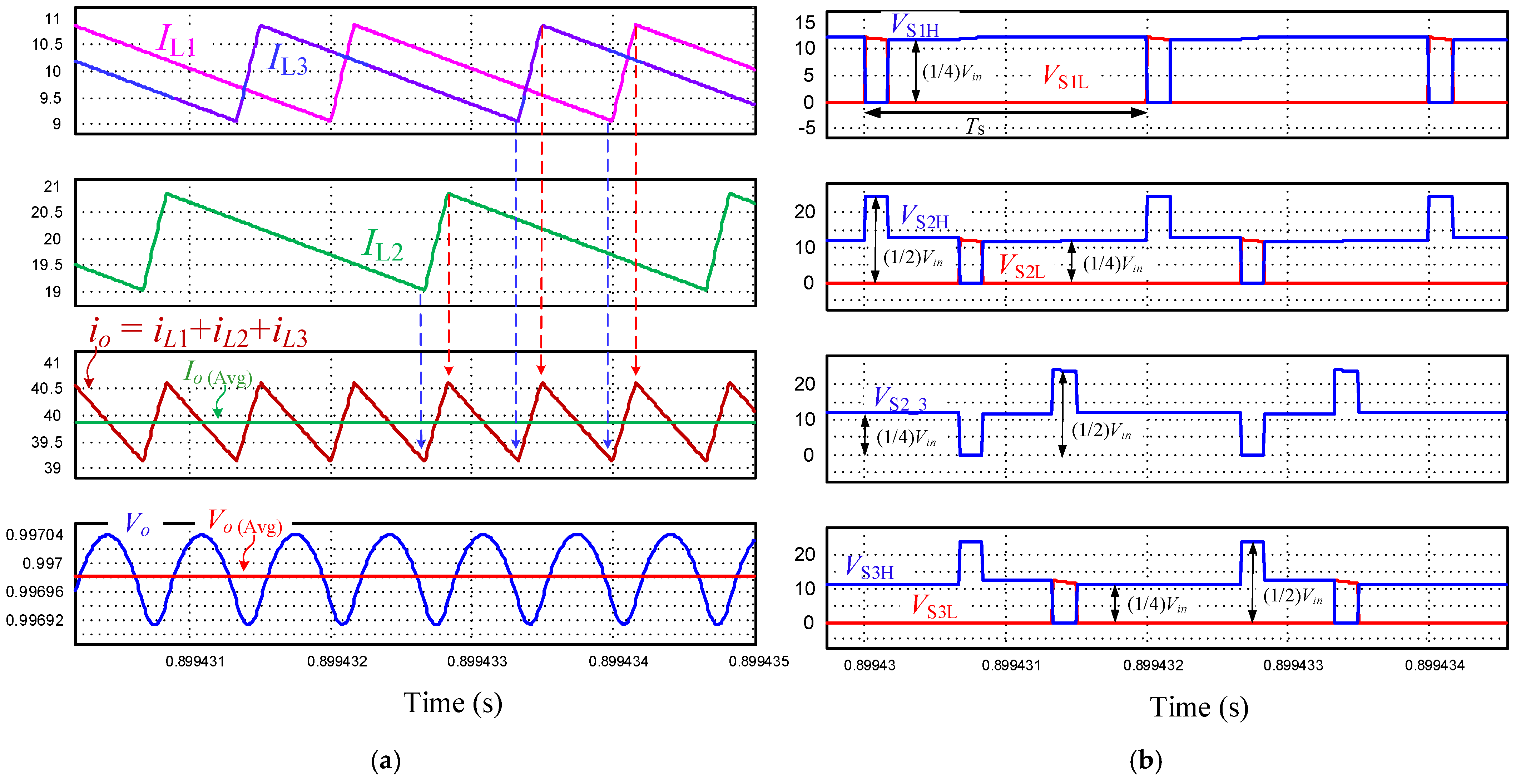
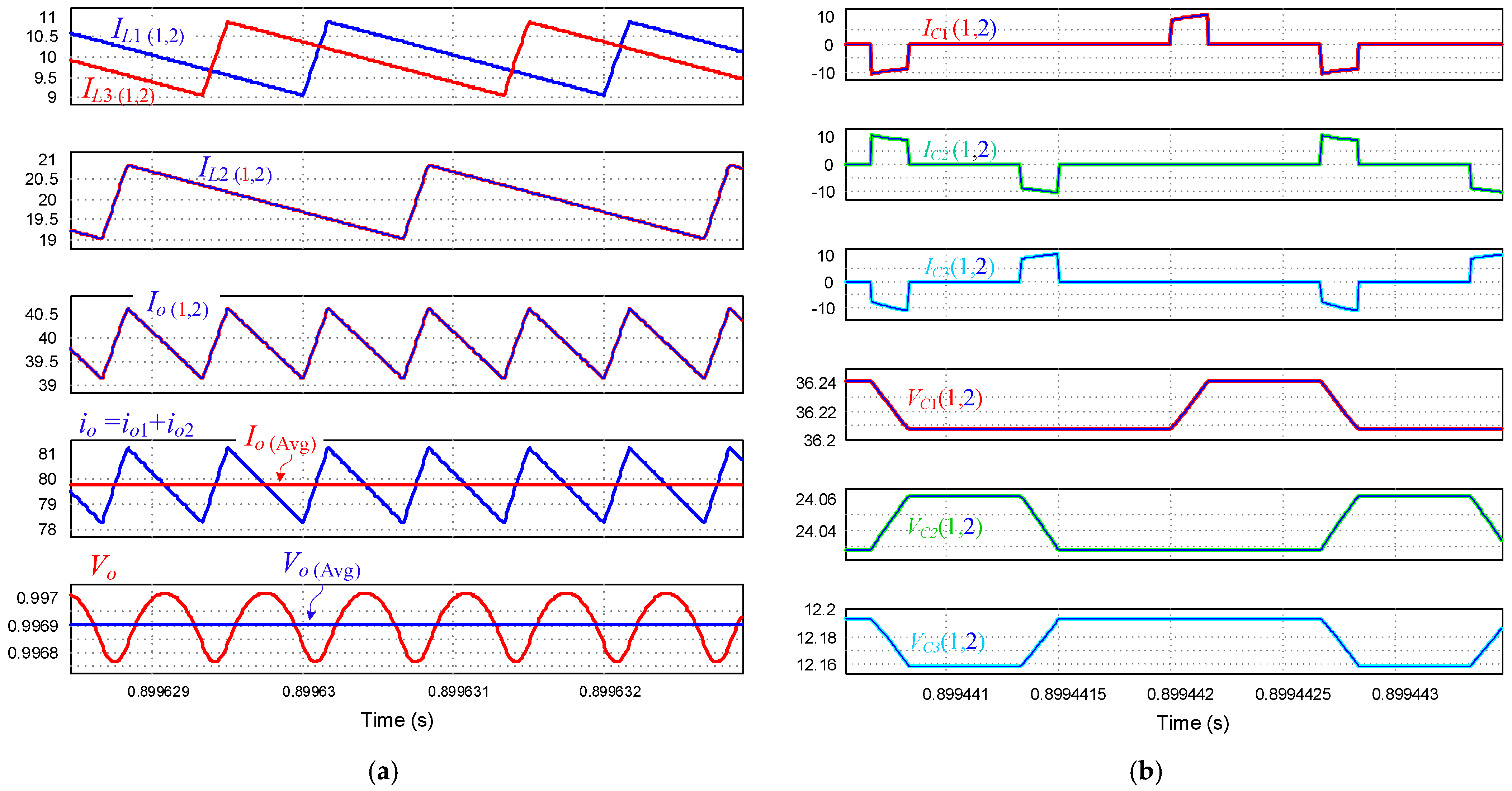
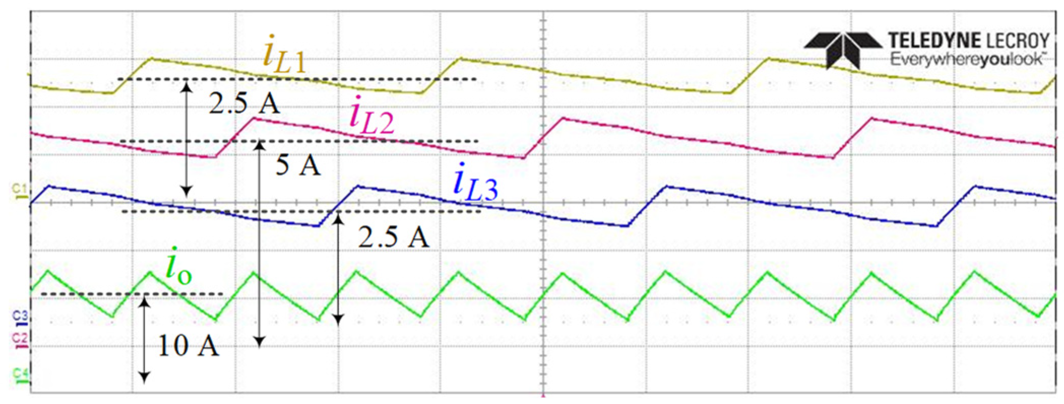
3.2. Inductors’ Currents and Balancing

For simplicity, it is assumed that the converter is loaded with a very light load at the output. The load current Iout is delivered from all three phases and equals to the sum of the average inductors’ currents. This relationship can be expressed by the following equation:
I out = I L 1 + I L 2 + I L 3 .
The average value of each of the inductor’s currents at a steady state can be calculated using the fact that the charge balance is achieved for each of the capacitors [54]. For example, the charge delivered to C2 during state III must be equal to the charge consumed from C2 (by C3) during state V. Thus, charge equations can be summarized as follows:
Q C 1 , 1 2 I L 2 D 2 f s charge =   I L 1 D 1 f s discharge , Q C 2 ,   1 2 I L 2 D 2 f s charge = I L 3 D 3 f s discharge ,   Q C 3 ,   I L 3 D 3 f s charge = 1 2 I L 2 D 2 f s discharge .
Solving the system using Equation (9) yields the average inductors’ currents:
I L 1 = D 2 D 3 D 2 D 3 + D 1 D 2 + 2 D 1 D 3 I out , I L 2 = 2 D 1 D 3 2 D 1 D 3 + D 2 D 3 + D 1 D 2 I out , I L 3 = D 1 D 2 D 2 D 3 + D 1 D 3 + 2 D 1 D 3 I out .
Therefore, in the most straightforward private case where duty cycles are equal, D1 = D2 = D3 = D, the three-phase converter average inductor currents become IL1 = Iout/4, IL2 = Iout/2 and IL3 = Iout/4. It should be mentioned that phase 2 carries double the current compared to phases 1 and 3. This is a result of both capacitors C1 and C3 discharging at state III, through inductor L2. The inductors’ current balance between phases can be achieved by setting the duty cycle of phase 2 to be half of the duty cycle of phases 1 and 3. The duty cycles in this case are summarized in (12), and the voltage ratio of the converter becomes M = D2/6 = D1/3.
D 1 = D 3 = D 2 / 2 .

3.3. Soft Charge/Discharge

The condition for soft charging is based on the ratio between each charging time and time constant of the capacitance loop [51,52,53]. When the switching time is much shorter than the time constant of the loop circuit, the current is practically constant during the switching time and hence the RMS value is the lowest possible. This condition can be expressed as follows:
T j < < R j C j ,
where Rj and Cj are the total ESR and capacitance in each switching state, respectively, and Tj is the time interval. Hard charging occurs when two branches of capacitors are connected in parallel. In the case of imperfect symmetry between the capacitor voltages in the circuit, state III (Figure 4) may experience hard switching for some short periods upon state changes. There, high current spikes may arise as a result of voltage mismatch between branches (C1 + C2 in parallel to C3). Applying generic cell structure in schematic and in physical layout are some of the measures to remedy this issue as it significantly reduces voltage mismatches due to parasitical elements. The use of low ESR capacitors is recommended to further reduce the potential voltage mismatch as a result of component uncertainties, when paralleling capacitors.

3.4. Switches Voltage Stress

The expression for maximum voltage stress across each of the converter switches during each converter state, along with an example of maximum voltage stresses in the application of 48 V-to-1 V (right most column), are summarized in Table 1. Low-side switches S1L, S2L, S3L, and S1H operate with a very low voltage stress of Vin/4, while the high-side switches S2H, S2-3, and S3H experience higher stresses of Vin/2 during one of the switching states. The maximum voltage stress values express the highest possible voltage that appears across the switch at any of the switching stages. The presence of the flying capacitors is the key factor in reducing the voltage stress across each of the MOSFETs, and the stress can be further reduced if a higher number of cells is used.

3.5. CCM–DCM Boundary

For a new converter operation in the continuous conduction mode (CCM), the inductor current needs to be always positive. The boundary between CCM and discontinuous conduction mode (DCM) is considered when the inductor current falls to zero at the end of the switching cycle. Setting the IL (min) to zero [48,49,50], results in an expression for the average inductor current for the CCM–DCM boundary:
I L ( a v ) = 1 T 1 2 I max D o n T + 1 2 I max D o f f T = 1 2 I max D o n + D o f f .
Assuming that the duty cycles are equal for all converter phases, the average current of inductors L1, L2, L3, can be expressed as IL1 = Vo/4Ro, IL2 = Vo/2Ro, and IL3 = Vo/4Ro, respectively, according to (11). At steady state, the ΔIL in the charge stage is equal to the discharged stage. For inductor L1, the expression for IL1(max) can be summarized as follows:
I L 1 ( max ) = V i n V C 1 V 0 L 1 D o n T ,
The boundary condition is calculated for each inductor from the charge or discharge equations using the expressions in (2), (3), and (4). Substituting (15) into (14), using Equation (2), and after some manipulations, the boundary condition can be summarized as follows:
V o 4 R o = V i n V c 1 V 0 2 L 1 D 1 o n T D 1 o n + D 1 o f f = = V 0 2 L 1 D 1 o f f T D 1 o n + D 1 o f f .
Note that at the boundary between the CCM to DCM modes, the sum of the duty ratios can still be written as D1on + D1off = 1; hence, Equation (16) can be also expressed as follows:
L 1 min = 2 R o 1 D 1 o n f S ,
where L1(min) is the minimum inductance required for CCM mode operation. The boundaries for L2 and L3 can be calculated using Equations (3), (4), (11), and (14), in the similar manner as described for L1. The expressions for L2 and L3 are summarized below:
L 2 min = R o 1 D 2 o n f S , L 3 min = 2 R o 1 D 3 o n f S .

4. Extension for Higher Order Converters

The cell of Figure 2 enables converter extension along multiple directions. The first extension addresses a higher conversion ratio. It is achieved by chaining several cells one after another. The number of cells is defined as n (Figure 5), and the chaining procedure follows the method outlined in Section 2, using the cell described in Figure 2, where all inductors are connected in parallel at the output, and the high-side voltage of the flying capacitor of a preceding cell connects to the high-side switch (SxH), of the next one (Figure 1). To provide a discharge path for the last cell capacitor, one additional switch per converter is added S(n–1)–(n) Figure 5.
The expression for the conversion ratio, in a generalized form for a single module with n cells in series, 1 × n topology, and assuming equal duty cycle is applied to all the cells, takes the form of (19):
M n = V o V i n = D n + 1 ,
where n is the number of cells of one converter module, and D is the common duty cycle applied to all the cells.
Average capacitor voltages per phase can be expressed as follows:
V C i = n ( i 1 ) n + 1 V i n ,
where i is the index of the cell number. For example, in a two-cell topology, n = 2 [20], the conversion ratio M is equal to M = D/3 and capacitor voltages are VC1 = 2Vin/3 and VC2 = Vin/3. For a three-phase case, n = 3, the ratio M equals to M = D/4, and the average capacitor voltages are VC1 = 3Vin/4, VC2 = 2Vin/4, and VC3 = Vin/4, as summarized in Section 3.1. The average inductors’ currents for each phase (except phase n-1) can be represented as follows:
I L i = 1 n + 1 I o u t ,
where the average inductor current for phase n-1 will be twice that of the other phases (assuming again equal duty cycle) due to a slightly different operation mode of the last two cells. For example, for a single module, m = 1, and two cells, n = 2, the average inductors currents are IL1 = Iout/3 and IL2 = 2Iout/3, and for the case of three cells, n = 3, inductors currents at steady state are IL1 = Iout/4, IL2 = Iout/2, and IL3 = Iout/4, as mentioned in Section 3.2.
The second extension covers the power capability of the converter, i.e., output current. Higher power to the load is facilitated by paralleling modules. Paralleling is carried out on the module level, where the inputs and the outputs of all the modules are connected in parallel to the source and the load, respectively. In this manner, the outputs of the modules share the same capacitor. The number of modules in parallel are referred to here as m (Figure 5).
The total output current in the case of the m × n system can be calculated by summing up all output currents from all the modules, where each module output current consists of the sum of its inductors currents. The expression for multi module total output current is summarized in (22):
I o u t T = Module = 1 m Ph   = 1 n I L ( P h )
A parallel connection of multiple modules can significantly lower the voltage and current component stresses, enabling a higher output power with better efficiency.
The third expansion provides a degree of freedom where the per-phase duty ratio is independently set. This assists in balancing the currents along the cells, facilitates targeted current sharing control that could be unbalanced, for example, and enables a better thermal management. The current mismatch between the phases can be adjusted by tuning the duty cycle of each phase, as mentioned in Section 3.2. An example of a three-phase converter response to non-equal duty cycle among the phases is demonstrated in Figure 6. Similar conversion ratios can be achieved by applying a different combination of D1, D2, and D3 (Figure 6a). Since, as mentioned earlier, the n-1 phase always carries double the current of the rest of the phases, in three-phase converter it makes sense to separate its duty cycle from the rest of the phases. This case is demonstrated in Figure 6b, where D1 and D3 are equal and being changed together (represented by the x axis). The solid traces represent the resulting conversion ratio of several selected duty cycles of the n-1 phase. Horizontal dashed red lines demonstrate three conversion ratios, and as can be observed, there are many intersections with the solid black traces, which are the operation points of different duty cycles that result in the same conversion ratio. Using this degree of freedom, the inherent current of the n-1 phase could be dialed down to be equal to the rest of the phases. This is beneficial since a current mismatch between phases and between modules can lead to a higher output current ripple. Taking advantage of these expansion possibilities offers three degrees of freedom in the converter architecture, allowing the design objectives to remain independent of one another. For example, going with a higher conversion ratio does not penalize the efficiency or phase balance of the converter.
The general expression for maximum voltage stress as a function of Vin across each of the converter switches, relative to the converter order, is summarized in Table 2. A higher converter order results in a lower voltage stress on both low-side and high-side switches. It is worth noting that low-side switches (SxL) conduct for much longer periods of time and as a result carry a much higher average current during the discharge states. They are exposed to twice as low a voltage stress as their high-side counterparts, allowing them to select a lower resistance switch to further reduce the losses. High-side switches (SxH)—except for S1H and S(n−1) – (n)—experience higher voltage stresses during one of the switching states.

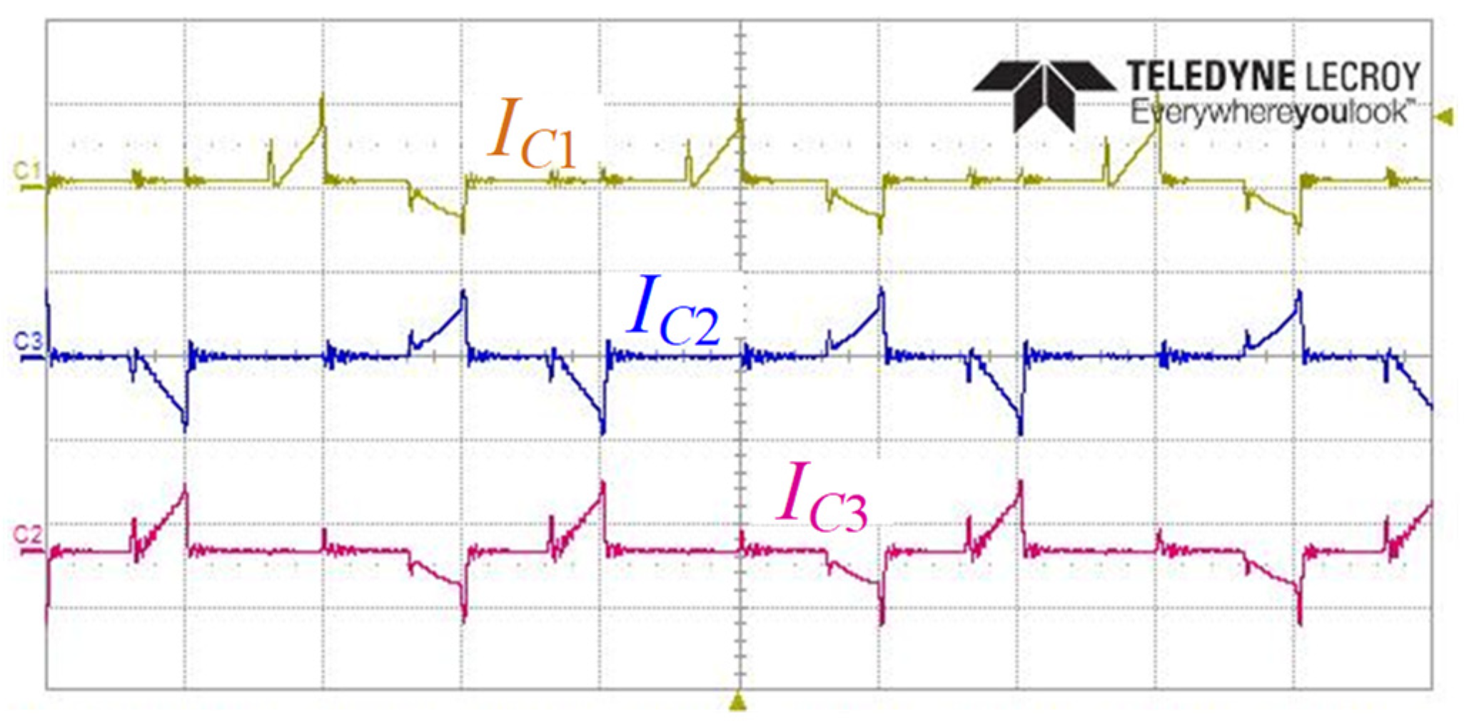
5. Simulation and Experimental Results

The verification and proof-of-concept demonstration of the design methodology are carried out by a simulation and experiments of a three-phase buck converter.
A steady-state simulation waveforms of 40 W, 48 V-to-1 V converter for an output current of 40 A with equal duty ratios of 1/12 is shown in Figure 7. The output voltage, inductors currents, and the sum of the inductor currents in the CCM mode are shown in Figure 7a. Note that due to the three-phase interleaved operation of the converter, the effective switching frequency at the output of the converter triples from 500 kHz to 1.5 MHz. From the results, natural current sharing is observed between phases and a ratio of 2:1 between IL2 to IL1 and IL3 can be seen. The simulation includes switch resistances RDS (on) as outlined in Table 3, so that the output voltage and current are slightly lower than theoretically expected. The maximum voltage stress of Vin/2 on the switches S2H, S2-3, and S3H is demonstrated in Figure 7b.
A simulation of a multiphase converter with two 1 × 3 modules is shown in Figure 8. The converter is rated at 80 W, steps the voltage down from 48 V-to-1 V, and operates at a switching frequency of 500 kHz per-phase. The converter consists of two modules (m = 2) that are connected in parallel, each with a chain of three cells (n = 3). Both converters are identical and operate with the same duty ratio that results in an output voltage of 1 V. Simulation results of Figure 8 demonstrate equal current levels and shapes for each of the modules, and the total output current is the sum of the two currents from each module, i.e., IoutT = Io1 + Io2.
To demonstrate the current sharing robustness of the topology in a presence of inductors mismatch, a simulation of the converter operating under heavy load conditions of Vin = 48 V, Vout = 1 V, and Iout = 100 A, with equal duty ratio and different inductance values of L1 = 0.6 µH, L2 = 0.2 µH, and L3 = 0.5 µH is shown in Figure 9. The simulation demonstrates a difference between L1 and L3 on the level of a component tolerance mismatch, and a major inductance disproportion is demonstrated using a very low inductance of L2 comparing to L1 and L3. The average currents are equal to IL1 = IL3 = Iout/4 = 25 A and IL2 = 2Iout/4 = 50 A, similar to the case of equal inductances, maintaining current sharing for even the high inductance difference. The change that could be observed is in the current ripple. It should be noted that a CCM operation mode needs to be maintained to ensure current sharing and overall correct converter operation.
To validate the operation of the three-phase topology at a high voltage and high conversion ratio, a 100 W laboratory prototype that operates at a switching frequency of 333 kHz per phase was built and tested. Table 3 lists the components’ values and nominal parameters of the experimental prototype. Each phase in the converter has been designed to be identical, as can be seen in the photograph of the experimental prototype (Figure 10). Each cell is comprised of an inductor, a flying capacitor that consists of two 10 µF capacitors connected in parallel to reduce the ESR, and a dual N-Channel MOSFET. A microchip dsPIC33 controller is used to generate complementary gate waveforms for switches SxL and SxH. The experiments are performed with an output voltage range of 1–1.5 V and maximum load of 100 A. Figure 11 shows the three-phase inductors currents and the output current, which is the sum of all three-inductors currents, (interleaved mode), i.e., Io = 10 A and Vo = 1.5 V. We measured average capacitors voltages, and the output voltages are VC1 ≈ 36 V, VC2 ≈ 24 V, VC3 ≈ 12 V, and Vo ≈ 1.5 V, as demonstrated in Figure 12, and fully support the theoretical derivations. The existence of soft charge has been demonstrated by measuring the capacitors currents (Figure 13). Please note that the minor spikes in Figure 13 are the result of a nonideal current measurement setup. The measured voltages on all the switches are shown in Figure 14. As can be seen from the experimental results, the maximum voltage stress on switches S1L, S2L, S1H, and S3L is Vin/4 and the maximum voltage stress on switches S2H, S2-3, and S3H is Vin/2. The results align well with the theoretical analysis that is summarized in Table 1. The power stage efficiency is shown in Figure 15. Three output voltages of 1.0 V, 1.2 V, and 1.5 V are demonstrated operating off a constant input voltage of 48 V.
Table 4 presents a performance review of state-of-the-art single-stage wide conversion ratio solutions and this work.

6. Conclusions

A modular construction approach of a very-high conversion ratio multiphase converter, based on a generic, switched LC cell is presented. The converter is built from a chain of identical building blocks, each consisting of a switched inductor–capacitor pair that forms a stacked series-capacitor converter at the input; while at the output, the converter has a structure of parallel or interleaved inductors. This modular stacking of generic cells allows flexibility in the design, enabling a high-power and high-conversion ratio without sacrificing the efficiency of the converter. It becomes possible due to the single-cycle power processing from the source to load operation principle, regardless of the number of modules stacked. Additional features of the architecture include the soft charging operation of the series capacitors, a voltage stress reduction of the switches due to the series capacitor’s structure, and current sharing across the phases. Current sharing is maintained throughout the multiphase output, allowing state-of-the-art performance in terms of power considerations and converter sizing for operation in both steady-state and transient modes. These characteristics contribute to a more compact system design and higher efficiency, particularly in direct 48 V-to-1.x V conversions, commonly required in data centers and other advanced applications. The performance of the proposed approach is validated through an interleaved three-phase modular prototype, which demonstrates excellent agreement with theoretical predictions and simulation results.
The technique of generic cell copying and multiplication presented here significantly reduces the complexity of the design and implementation of switched-mode power converters for multiple use cases. The concept of generalization extends the capability of supporting higher currents and power by connecting the m number of modules in parallel. Mismatches between phases or between modules can be adjusted by controlling the duty cycle of each cell independently if needed. The resulting architecture enables one to seamlessly achieve any conversion ratio using identical cells or modules. This ultimately establishes the enabling technology for reliable, fast, and power-oriented design of high conversion ratio power-converters, as a new baseline in the field.

Author Contributions

Conceptualization, E.H. and M.M.P.; methodology, E.H. and M.M.P.; software and hardware, E.H.; validation, E.H.; formal analysis, E.H., M.E., and M.M.P.; investigation, E.H., M.E. and M.M.P.; writing—original draft preparation, E.H., M.E. and M.M.P.; writing—review and editing, E.H., M.E. and M.M.P.; supervision, M.M.P. All authors have read and agreed to the published version of the manuscript.

Funding

This research received no external funding.

Institutional Review Board Statement

Not applicable.

Informed Consent Statement

Not applicable.

Data Availability Statement

The original contributions presented in this study are included in the article. Further inquiries can be directed to the corresponding author.

Conflicts of Interest

The authors declare no conflicts of interest.

References

  1. Ericsson Mobility Report. Available online: https://www.ericsson.com/en/mobility-report/reports (accessed on 20 June 2021).
  2. NRDC. Data Center Efficiency Assessment. Available online: https://www.nrdc.org/sites/default/files/data-center-efficiency-assessment-IP.pdf (accessed on 5 August 2014).
  3. Dayarathna, M.; Wen, Y.; Fan, R. Data center energy consumption modeling: A survey. IEEE Commun. Surv. Tutor. 2016, 18, 732–794. [Google Scholar] [CrossRef]
  4. Dumitrescu, C.; Pleşca, A. Overview on energy efficiency parameters in data centers. In Proceedings of the 2016 International Conference and Exposition on Electrical and Power Engineering (EPE), Iasi, Romania, 20–22 October 2016; pp. 153–156. [Google Scholar]
  5. Frachtenberg, E. Holistic datacenter design in the open compute project. Computer 2012, 45, 83–85. [Google Scholar] [CrossRef]
  6. Ahmed, M.H.; Fei, C.; Lee, F.C.; Li, Q. 48-V voltage regulator module with PCB winding matrix transformer for future data centers. IEEE Trans. Ind. Electron. 2017, 64, 9302–9310. [Google Scholar] [CrossRef]
  7. Ye, Z.; Lei, Y.; Pilawa-Podgurski, R.C.N. The cascaded resonant converter: A hybrid switched-capacitor topology with high power density and efficiency. IEEE Trans. Power Electron. 2020, 35, 4946–4958. [Google Scholar] [CrossRef]
  8. Liu, W.C.; Ye, Z.; Pilawa-Podgurski, R.C.N. A 97% peak efficiency and 308 A/in3 current density 48-to-4 V two-stage resonant switched capacitor converter for data center applications. In Proceedings of the 2020 IEEE Applied Power Electronics Conference and Exposition (APEC), New Orleans, LA, USA, 15–19 March 2020; pp. 468–474. [Google Scholar]
  9. Liu, W.C.; Pilawa-Podgurski, R.C. Bi-lateral energy resonant converter (berc) with merged two-stage inductor for 48-to-12V applications. In Proceedings of the 2020 IEEE 21st Workshop on Control and Modeling for Power Electronics (COMPEL), Aalborg, Denmark, 30 November 2020; pp. 1–6. [Google Scholar]
  10. Baek, J.; Wang, P.; Elasser, Y.; Chen, Y.; Jiang, S.; Chen, M. Legopol: A 48V-1.5V 300A merged-two-stage hybrid converter for ultrahigh-current microprocessors. In Proceedings of the 2020 IEEE Applied Power Electronics Conference and Exposition (APEC), New Orleans, LA, USA, 15–19 March 2020; pp. 490–497. [Google Scholar]
  11. Ursino, M.; Saggini, S.; Jiang, S.; Nan, C. High density 48V-to-PoL VRM with hybrid pre-regulator and fixed-ratio buck. In Proceedings of the 2020 IEEE Applied Power Electronics Conference and Exposition (APEC), New Orleans, LA, USA, 15–19 March 2020; pp. 498–505. [Google Scholar]
  12. Ye, Z.; Abramson, R.A.; Syu, Y.L.; Pilawa-Podgurski, R.C.N. MLB-PoL: A high-performance hybrid converter for direct 48 V to point-of-load applications. In Proceedings of the 2020 IEEE 21st Workshop on Control and Modeling for Power Electronics (COMPEL), Aalborg, Denmark, 30 November 2020. [Google Scholar]
  13. Batarseh, M.; Wang, X.; Batarseh, I. Nonisolated half bridge buck-based converter for VRM application. In Proceedings of the 2007 IEEE Power Electronics Specialists Conference, Orlando, FL, USA, 17–21 June 2007; pp. 2393–2398. [Google Scholar]
  14. Oraw, B.S.; Ayyanar, R. Voltage regulator optimization using multi winding coupled inductors and extended duty ratio mechanisms. IEEE Trans. Power Electron. 2009, 24, 1494–1505. [Google Scholar] [CrossRef]
  15. Xu, M.; Sun, J.; Lee, F.C. Voltage divider and its application in the two-stage power architecture. In Proceedings of the Twenty-First Annual IEEE Applied Power Electronics Conference and Exposition, APEC’06, Dallas, TX, USA, 19–23 March 2006; pp. 499–505. [Google Scholar]
  16. Ye, Z.; Abramson, R.A.; Pilawa-Podgurski, R.C.N. A 48-to-6V multi-resonant-doubler switched-capacitor converter for data center applications. In Proceedings of the 2020 IEEE Applied Power Electronics Conference and Exposition (APEC), New Orleans, LA, USA, 15–19 March 2020; pp. 475–481. [Google Scholar]
  17. Abramson, R.A.; Ye, Z.; Pilawa-Podgurski, R.C.N. A high performance 48-to-8 v multi-resonant switched-capacitor converter for data center applications. In Proceedings of the 2020 22nd European Conference on Power Electronics and Applications (EPE’20 ECCE Europe), Lyon, France, 7–11 September 2020; pp. 1–10. [Google Scholar]
  18. Ahmed, M.H.; Fei, C.; Lee, F.C.; Li, Q. Single-stage high-efficiency 48/1 V sigma converter with integrated magnetics. IEEE Trans. Ind. Electron. 2020, 67, 192–202. [Google Scholar] [CrossRef]
  19. Halamicek, M.; McRae, T.; Prodić, A. Cross-coupled series-capacitor quadruple step-down buck converter. In Proceedings of the 2020 IEEE Applied Power Electronics Conference and Exposition (APEC), New Orleans, LA, USA, 15–19 March 2020. [Google Scholar]
  20. Kirshenboim, O.; Peretz, M.M. High-efficiency nonisolated converter with very high step-down conversion ratio. IEEE Trans. Power Electron. 2017, 32, 3683–3690. [Google Scholar] [CrossRef]
  21. Das, R.; Seo, G.; Maksimovic, D.; Le, H.P. An 80-w 94.6%-efficient multi-phase multi-inductor hybrid converter. In Proceedings of the 2019 IEEE Applied Power Electronics Conference and Exposition (APEC), Anaheim, CA, USA, 17–21 March 2019; pp. 1–6. [Google Scholar]
  22. Das, R.; Le, H.P. A Regulated 48V-to-1V/100A 90.9%-Efficient Hybrid Converter for POL Applications in Data Centers and Telecommunication Systems. In Proceedings of the 2019 IEEE Applied Power Electronics Conference and Exposition (APEC), Anaheim, CA, USA, 17–21 March 2019; pp. 1997–2001. [Google Scholar]
  23. Jang, Y.; Jovanovic, M.M.; Panov, Y. Multi-phase buck converters with extended duty cycle. In Proceedings of the Twenty-First Annual IEEE Applied Power Electronics Conference and Exposition, APEC’06, Dallas, TX, USA, 19–23 March 2006; pp. 38–44. [Google Scholar]
  24. Youssef, M.; Jain, P.K. Analysis and design of a novel LLC 48V resonant self-oscillating voltage regulator module. In Proceedings of the 2007 IEEE Power Electronics Specialists Conference, Orlando, FL, USA, 17–21 June 2007; pp. 252–258. [Google Scholar]
  25. Youssef, M.; Jain, P.K. A 48V resonant voltage regulator module with a new current mode controller. In Proceedings of the 2006 37th IEEE Power Electronics Specialists Conference, Jeju, Republic of Korea, 18–22 June 2006; pp. 1–7. [Google Scholar]
  26. Jang, Y.; Jovanovic, M.M.; Panov, Y. Nonisolated Power Conversion System Having Multiple Switching Power Converters. U.S. Patent 7 230 405, 12 June 2007. [Google Scholar]
  27. Abe, K.; Nishijima, K.; Harada, K.; Nakano, T.; Nabeshima, T.; Sato, T. A novel three-phase buck converter with bootstrap driver circuit. In Proceedings of the 2007 IEEE Power Electronics Specialists Conference, Orlando, FL, USA, 17–21 June 2007; pp. 1864–1871. [Google Scholar]
  28. Nishijima, K.; Harada, K.; Nakano, T.; Nabeshima, T.; Sato, T. Analysis of double step-down two-phase buck converter for VRM. In Proceedings of the INTELEC 05-Twenty-Seventh International Telecommunications Conference, Berlin, Germany, 18–22 September 2005; pp. 497–502. [Google Scholar]
  29. Matsumoto, K.; Nishijima, K.; Sato, T.; Nabeshima, T. A two-phase high step down coupled-inductor converter for next generation low voltage CPU. In Proceedings of the 8th International Conference on Power Electronics-ECCE Asia, Jeju, Republic of Korea, 30 May–3 June 2011; pp. 2813–2818. [Google Scholar]
  30. Chuang, C.F.; Pan, C.T.; Cheng, H.C. A novel transformer-less interleaved four-phase step-down DC converter with low switch voltage stress and automatic uniform current-sharing characteristics. IEEE Trans. Power Electron. 2016, 31, 406–417. [Google Scholar] [CrossRef]
  31. Shanoy, P.S.; Amaro, M.; Morroni, J.; Freeman, D. Comparison of a buck converter and a series capacitor buck converter for high frequency, high conversion ratio voltage regulators. IEEE Trans. Power Electron. 2016, 31, 7006–7015. [Google Scholar] [CrossRef]
  32. Lee, I.O.; Cho, S.Y.; Moon, G.W. Interleaved buck converter having low switching losses and improved step-down conversion ratio. IEEE Trans. Power Electron. 2012, 27, 3664–3675. [Google Scholar] [CrossRef]
  33. Jain, P.; Prodic, A.; Gerfer, A. Wide-input high power density flexible converter topology for DC-DC applications. In Proceedings of the 2016 IEEE Applied Power Electronics Conference and Exposition (APEC), Long Beach, CA, USA, 20–24 March 2016; pp. 2553–2560. [Google Scholar]
  34. Hamo, E.; Evzelman, M.; Peretz, M.M. High-Conversion Ratio Multi-Phase VRM Realized with Stacking of Generic Series-Capacitor-Buck Converter Cells. In Proceedings of the 2022 IEEE 23rd Workshop on Control and Modeling for Power Electronics (COMPEL), Tel Aviv, Israel, 20–23 June 2022; pp. 1–6. [Google Scholar]
  35. Ahsanuzzaman, S.M.; Ma, Y.; Pathan, A.A.; Prodic, A. A low-volume hybrid step-down DC-DC converter based on the dual use of flying capacitor. In Proceedings of the 2016 IEEE Applied Power Electronics Conference and Exposition (APEC), Long Beach, CA, USA, 20–24 March 2016; pp. 2497–2503. [Google Scholar]
  36. Meynard, T.A.; Foch, H. Multilevel converters and derived topologies for high power conversion. In Proceedings of the IECON’95—21st Annual Conference on IEEE Industrial Electronics, Orlando, FL, USA, 6–10 November 1995; pp. 21–26. [Google Scholar]
  37. Du, X.; Zhou, L.; Tai, H.M. Double-frequency buck converter. IEEE Trans. Ind. Electron. 2009, 56, 1690–1698. [Google Scholar]
  38. Middlebrook, R.D. Transformerless DC-to-DC converters with large conversion ratios. IEEE Trans. Power Electron. 1988, 3, 484–488. [Google Scholar] [CrossRef]
  39. Oraw, B.; Ayyanar, R. Small signal modeling and control design for new extended duty ratio, interleaved multiphase synchronous buck converter. In Proceedings of the INTELEC 06-Twenty-Eighth International Telecommunications Energy Conference, Providence, RI, USA, 10–14 September 2006; pp. 1–8. [Google Scholar]
  40. Radić, A.; Prodić, A. Buck converter with merged active charge-controlled capacitive attenuation. IEEE Trans. Power Electron. 2012, 27, 1049–1054. [Google Scholar] [CrossRef]
  41. Roberts, G.; Prodić, A. Modulation improvements for high-phase-count series-capacitor buck converters. IEEE Open J. Power Electron. 2024, 5, 1071–1092. [Google Scholar] [CrossRef]
  42. Naradhipa, A.M.; Li, Q. Partial phase overlap control for multiphase series capacitor buck converter. In Proceedings of the 2023 IEEE 24th Workshop on Control and Modeling for Power Electronics (COMPEL), Ann Arbor, MI, USA, 25–28 June 2023; pp. 1–7. [Google Scholar]
  43. Li, C.Y.; Nien, C.F.; Lin, L.; Chen, H.C. A generalized current balancing control for series-capacitor buck converter with interleaved phase angle. In Proceedings of the 2023 IEEE 24th Workshop on Control and Modeling for Power Electronics (COMPEL), Ann Arbor, MI, USA, 25–28 June 2023; pp. 1–5. [Google Scholar]
  44. Majumder, P.; Kapat, S.; Kastha, D. Fast transient state feedback digital current mode control design in series capacitor buck converters. In Proceedings of the 2022 IEEE Applied Power Electronics Conference and Exposition (APEC), Houston, TX, USA, 20–24 March 2022; pp. 2080–2085. [Google Scholar]
  45. Wang, Z.; Fang, P. Modular series capacitor buck topology for point of load applications with duty cycle freer. In Proceedings of the 2023 IEEE 24th Workshop on Control and Modeling for Power Electronics (COMPEL), Ann Arbor, MI, USA, 25–28 June 2023; pp. 1–8. [Google Scholar]
  46. Ibarra, E.; Arias, A.; de Alegría, I.M.; Otero, A.; de Mallac, L. Digital control of multiphase series capacitor buck converter prototype for the powering of HL-LHC inner triplet magnets. IEEE Trans. Ind. Electron. 2022, 69, 10014–10024. [Google Scholar] [CrossRef]
  47. Yousefzadeh, V.; Alarcon, E.; Maksimovic, D. Three-level buck converter for envelope tracking applications. IEEE Trans. Power Electron. 2006, 21, 549–552. [Google Scholar] [CrossRef]
  48. Muhammad, H.R. Power Electronics: Circuits, Devices and Applications; Prentice-Hall: Hoboken, NJ, USA, 1993. [Google Scholar]
  49. Mohan, N.; Undeland, T.M.; Robbins, W.P. Power Electronics; Wiley: Hoboken, NJ, USA, 2003. [Google Scholar]
  50. Hart, D.W. Power Electronics; McGraw-Hill: New York, NY, USA, 2011. [Google Scholar]
  51. Shenoy, P.S.; Lazaro, O.; Amaro, M.; Ramani, R.; Wiktor, W.; Lynch, B.; Khayat, J. Automatic current sharing mechanism in the series capacitor buck converter. In Proceedings of the 2015 IEEE Energy Conversion Congress and Exposition (ECCE), Montreal, QC, Canada, 20–24 September 2015; pp. 2003–2009. [Google Scholar]
  52. Lei, Y.; Pilawa-Podgurski, R.C.N. A general method for analyzing resonant and soft-charging operation of switched-capacitor converters. IEEE Trans. Power Electron. 2015, 30, 5650–5664. [Google Scholar] [CrossRef]
  53. Evzelman, M.; Ben-Yaakov, S. Average-current-based conduction losses model of switched capacitor converters. IEEE Trans. Power Electron. 2013, 28, 3341–3352. [Google Scholar] [CrossRef]
  54. Hamo, E.; Evzelman, M.; Peretz, M.M. Modeling and analysis of resonant switched-capacitor converters with free-wheeling ZCS. IEEE Trans. Power Electron. 2015, 30, 4952–4959. [Google Scholar] [CrossRef]
  55. Texas Instruments. Multiphase Buck Design from Start to Finish. Application Report 2021. Available online: https://www.ti.com/lit/an/slva882b/slva882b.pdf?ts=1748214604321&ref_url=https%253A%252F%252Fwww.google.com%252F (accessed on 10 May 2025).
Figure 1. Circuit diagram of three-cell buck converter.
Applsci 15 06818 g001
Figure 2. Generic LC cell for a modular multiphase converter.
Applsci 15 06818 g002
Figure 3. Timing diagram and idealized waveforms of a three-phase converter.
Applsci 15 06818 g003
Figure 4. Operation states I-VI. (a) State I: phase 1 is ON, and phases 2 and 3 are OFF. (b) States II, IV and V: all phases are OFF. (c) States III: phase 2 is ON, phases 1 and 3 are OFF. (d) State V: phase 3 is ON, phases 1 and 2 are OFF.
Applsci 15 06818 g004
Figure 5. Circuit diagram of a multiphase buck converters topology of an m × n order.
Applsci 15 06818 g005
Figure 6. The voltage ratio (1/M) of the presented topology according to Equation (6): (a) a continuous combination of D1 and D2 ranging from 0.05 to 0.25, with two constant values of D3 (0.05 and 0.25); (b) a case where D1 = D3 and are the x axis, and black solid traces represent several D2 values. Dashed red traces represent some conversion ratios and demonstrate the flexibility of the converter to achieve the same conversion ratio with several different duty ratio options.
Applsci 15 06818 g006
Figure 7. Simulation results of a single module where all duty cycles are equal: (a) top and second from the top plots—inductors currents, second from the bottom plot—output current, bottom plot—output voltage; (b) the voltages across all the switches: S1L, S1H, S2L, S2H, S2-3, S3L, and S3H.
Applsci 15 06818 g007
Figure 8. Simulation results of a multiphase buck converter that consists of two (m = 2) three-phase (n = 3) modules, denoted 1 and 2, where all duty cycles are equal. The simulation demonstrates: (a) output voltage, output current and inductors currents, and (b) capacitors currents in soft charge/discharge mode and capacitors voltages. The currents and voltages per module are marked by numbers inside the brackets.
Applsci 15 06818 g008
Figure 9. Simulation results for the heavy load conditions and unbalanced inductances, where L1 = 0.6 µH, L2 = 0.2 µH and L3 = 0.5 µH, Vout = 1 V, Iout = 100 A.
Applsci 15 06818 g009
Figure 10. Experimental prototype PCB: (a) The top view of the power stage that includes a microcontroller, one dual N-Channel MOSFET per cell, power inductors, and flying capacitors. (b) The bottom view that includes a buffer, drivers, and isolated DC/DC supplies.
Applsci 15 06818 g010
Figure 11. Experimental results: inductors’ current waveforms, C1 (yellow)—inductor current of L1 (2 A/div), C2 (red)—inductor current of L2 (2 A/div), C3 (blue)—inductor current of L3 (2 A/div), C4 (green)—output current (5 A/div). Horizontal scale (1 μs/div). Inductor phases are interleaved by 120 degrees.
Applsci 15 06818 g011
Figure 12. Experimental results: capacitors DC level measurements, C1 (yellow)—capacitor C1 voltage (20 V/div), C2 (red)—capacitor C2 voltage (20 V/div), C3 (blue)—capacitor C3 voltage (10 V/div), C4 (green)—output voltage (1 V/div).
Applsci 15 06818 g012
Figure 13. Experimental results: capacitors current measurements, C1 (yellow)—capacitor C1 current, C2 (red)—capacitor C3 current, C3 (blue)—capacitor C2 current, all channels are 12 A/div.
Applsci 15 06818 g013
Figure 14. Experimental results: switches voltages, (a) C1 (yellow)—switch S1L voltage, C2 (red)—S1H voltage, C3 (blue)—S2L voltage, C4 (green)—S2H voltage, all channels are 15 V/div. (b) C1 (yellow)—switch S2-3 voltage, C2 (red)—S3L voltage, C3 (blue)—S3H voltage, all channels are 15 V/div.
Applsci 15 06818 g014
Figure 15. Efficiency results from experimental measurements for different output voltages.
Applsci 15 06818 g015
Table 1. Switches voltages of each state in the 3ph. converter.
StateStress
(Vin = 48 V, M = 1/48)
SwitchIIIIIIIVVVIVmax [V]
S1LVin-VC10000012
S1H0Vin-VC1Vin-VC1Vin-VC1Vin-VC1Vin-VC112
S2L00VC300012
S2HVin-VC2VC1-VC20VC1-VC2VC1-VC2VC1-VC224
S2-3VC3VC30VC3VC2VC324
S3L0000VC2-VC3012
S3HVC2-VC3VC2-VC3VC2VC2-VC30VC2-VC324
The blue shade indicates the highest stress per switch.
Table 2. An example of maximum switch voltages vs. the number of cells.
# of Cells2345678
Switch
SxL (x ≥ 1) 1(1/3)Vin(1/4)Vin(1/5)Vin(1/6)Vin(1/7)Vin(1/8)Vin(1/9)Vin
SxH (x > 1) 2(2/3)Vin(2/4)Vin(2/5)Vin(2/6)Vin(2/7)Vin(2/8)Vin(2/9)Vin
1 Includes S1H; 2 includes the switch between the last cell to the previous one, S(n−1) – (n).
Table 3. Experimental prototype parameters.
Power Stage
ComponentP/NValue/Type
Input voltage-Vin 48 V
Output voltage-Vout 1–1.5 V
Switching freq.-fsw 333 kHz per Ph.
Input capacitor-CinEEE-FK2A221AV220 µF, 100 V
Output capacitor-CoutEEF-GX0D561R560 µF, 2 V
Inductors-L1, L2, L3XAL1580_401MEB0.4 µH, 60 A
Capacitors-C1, C2, C3C5750X7S2A106M10 µF, 100 V
MOSFETs (RDS on)NVMFD5C446NL2.2 mΩ, 145 A
Load resistance-Rload 10–100 mΩ
Floating Driver
Driver2EDF7275F
Isolated DC/DCTDR 3-1212SM
Digital Section
MicrocontrollerdsPIC33FJ16GS50216 bit, 40 MIPS
Buffers and DriversMC74VHC244DWR2G
Table 4. A performance review of state-of-the-art single-stage wide conversion ratio solutions.
Topology
/Reference
Voltage
Ratio
(Vo/Vin)
Regulated Tested Range
(Vin to Vo)
# L 1# C 1 Capacitors Stress 2Active
Components
Switches Stress 2
(Vblocking)
Peak Efficiency [%]
(Power Stage)
This Work
-x3 LC Cells
D/4Yes48 to 1–1.8 V33(3Vin/4), (Vin/2), (Vin/4) 7 SW5 × (Vin/4), 2 × (Vin/2)97.8 (40 A/1.8 V)
95.6 (38 A/1 V)
Multiphase Buck-5ph. [55]DYes12 to 1.8 V50--10 SW10 × (Vin)94.8 (55 A/1.8 V)
Series Cap Buck-3ph. [27]D/3Yes19 to 1.2 V;
16.8 to 0.9 V
32(2Vin/3), (Vin/3) 6 SW2 × (2Vin/3), 4 × (Vin/3)93 (5 A/1.2 V)
Multi-Resonant-
Doubler [16]
Fixed-
ratio
No48 to 6 V13(4Vo), (2Vo), (Vo)10 SW4 × (4Vo), 3 × (2Vo), 3 × (Vo)98.6 (5 A/6 V)
Multi-Resonant Cascaded Series-Parallel Converter [17]Fixed-
ratio
No48 to 8 V131 × (3Vo), 2 × (Vo)10 SW4 × (3Vo), 2 × (2Vo), 4 × (Vo)99 (5 A/8 V)
Cross-Coupled Series-Capacitor Quadruple Buck Converter [19]D/4Yes48 to 1 V231 × (Vin/2), 2 × (Vin/3)8 SW,
2x Diodes
6 × (Vin/4), 2 × (Vin/2)94.5 (15 A/1 V) 95.1 (17 A/1.8 V)
Seven-Level Multiphase Multi-Inductor Hybrid Converter [21]D/6Yes48 to 1–2 V35(5Vin/6), (4Vin/6), (3Vin/6), (2Vin/6), (Vin/6)9 SWNA94.6 (8 A/2 V) 92 (7 A/1 V)
1 The total number of inductors or capacitors in the power stage. 2 The stress on the capacitors and switches is quantified as the product of the number of components and their respective voltage stress. For example, the stress is calculated as N × (Vin/k), where N capacitors or switches equally share a voltage stress of Vin/k.
Disclaimer/Publisher’s Note: The statements, opinions and data contained in all publications are solely those of the individual author(s) and contributor(s) and not of MDPI and/or the editor(s). MDPI and/or the editor(s) disclaim responsibility for any injury to people or property resulting from any ideas, methods, instructions or products referred to in the content.

