Article

Simplified Derivative-Based Carrierless PPM Using VCO and Monostable Multivibrator

1
School of Engineering, King Mongkut’s Institute of Technology Ladkrabang, Bangkok 10520, Thailand
2
School of Integrated Innovative Technology, King Mongkut’s Institute of Technology Ladkrabang, Bangkok 10520, Thailand
3
School of Information Technology, King Mongkut’s Institute of Technology Ladkrabang, Bangkok 10520, Thailand
*
Author to whom correspondence should be addressed.
Appl. Sci. 2025, 15(11), 6272; https://doi.org/10.3390/app15116272
Submission received: 21 April 2025 / Revised: 30 May 2025 / Accepted: 30 May 2025 / Published: 3 June 2025

Abstract

:
This study proposes a derivative-based, carrierless pulse position modulation (PPM) scheme utilizing a voltage-controlled oscillator (VCO) and a monostable multivibrator. In contrast to conventional PPM systems that rely on reference carriers or complex demodulation methods, the proposed architecture simplifies signal generation by directly modulating the time derivative of the message signal. The modulated signal, when processed through standard analog demodulators, inherently yields the derivative of the original message. This behavior is first established through theoretical derivations and then confirmed by simulations and circuit-level experiments. The proposed method includes a differentiator feeding into a VCO, followed by a monostable multivibrator to generate a carrierless PPM waveform. Experimental validation confirms that, under all tested demodulation approaches—integrator-based, PLL-based, and quasi-FM—the recovered output aligns with the differentiated message signal. The integration of this output to retrieve the original message was not performed to maintain focus on verifying the modulation principle. Additionally, the study aimed to ensure the consistency of derivative recovery. Signal-to-noise ratio (SNR) expressions for each demodulator type are presented and discussed in the context of their relevance to the proposed system. Limitations and directions for further study are also identified.

1. Introduction

Pulse Position Modulation (PPM) is a well-established technique in optical and wireless communication [1], encoding information through the temporal position of pulses. PPM is traditionally classified into carrier-based and carrierless types. Carrier-based methods, while effective, depend on reference signals, which add to system complexity. Carrierless PPM avoids reference signals but often requires elaborate demodulation systems such as phase-locked loops (PLLs) [2], time-to-voltage converters, or signal reconstruction circuits.
In this study, we propose a novel carrierless PPM modulation scheme based on the derivative of the input signal, a voltage-controlled oscillator (VCO), and a monostable multivibrator. This architecture eliminates the need for carrier generation or reconstruction, enabling a simple and compact implementation. Using Fourier analysis, we demonstrate that carrierless PPM inherently encodes the derivative of the message signal in its lowest frequency component. This allows signal recovery using basic analog operations, such as integration and low-pass filtering, without requiring complex recovery circuits.
The approach contributes to both the theoretical understanding and practical realization of simplified modulation systems by offering a direct mapping from the input signal to carrierless PPM using minimal analog components. The remainder of this paper outlines the theoretical basis, proposed circuit design, and simulation-based validation of the method.

1.1. Literature Review

PPM has evolved across various communication domains, including optical fiber, free-space optics, and underwater laser communication [3,4,5,6,7]. It has been implemented in analog and digital forms [8], with innovations targeting improved synchronization [9], demodulation accuracy [10], and bandwidth efficiency [11,12]. Recent designs have integrated PPM with OFDM, PWM, and other hybrid schemes [13,14], aiming to increase spectral efficiency and robustness.
Traditional PPM demodulation involves converting received signals into PWM, then applying low-pass filtering or integrating them for message recovery [15,16]. These methods are straightforward for carrier-based PPM, but carrierless variants require additional processing, such as carrier reconstruction using PLLs or time-to-voltage conversion techniques [17,18,19,20,21,22]. Other studies explore PFM and selective pulse methods to improve demodulation flexibility [23,24].
Spectral analyses confirm that both PWM and PPM belong to the phase modulation family, though practical implementations remain complex. Hybrid modulation schemes and energy-efficient transceivers have shown performance gains, but with increased circuit intricacy [25,26,27,28,29].
While the building blocks used in this study—taking the derivative of the message signal, voltage-controlled oscillators, and monostable multivibrators—are well-established, this work draws insight from common principles across multiple PPM demodulation strategies to construct a new, low-complexity carrierless PPM modulation scheme. The resulting architecture eliminates carrier reconstruction and aligns well with compact, cost-sensitive platforms such as Internet of Things (IoT) systems [30]. By integrating foundational concepts in a novel configuration, this approach addresses implementation challenges in carrierless PPM and demonstrates practical advantages.
Several studies have analyzed pulse position modulation (PPM) in terms of bandwidth trade-offs, implementation complexity, and modulation comparisons. While many existing techniques rely on digital processing, complex synchronization, or hybrid signal processing, the proposed method adopts a refined analog design with a differentiator, VCO, and monostable multivibrator. Table 1 provides a concise overview of relevant works, including various implementation approaches. In contrast, the proposed technique leverages a practical design, offering a carrierless and hardware-optimized solution for pulse position modulation.

1.2. Research Contributions

The key contributions of this research are:
  • To develop a unified analytical framework showing that PPM demodulation fundamentally yields the derivative of the message signal.
  • To analyze and compare several carrierless PPM demodulation methods, confirming their inherent link to the derivative of the message signal.
  • To propose and implement a novel PPM modulation scheme where the differentiated message signal drives a VCO and monostable multivibrator, streamlining carrierless PPM generation.
  • To validate the proposed approach through simulations and experiments, demonstrating effective signal recovery and highlighting performance benefits over conventional methods in tested scenarios.
This paper is organized as follows. Section 2 presents a signal component analysis of PWM and PPM, establishing their mathematical and spectral properties. Section 3 derives the proposed derivative-based carrierless PPM method—employing a VCO and monostable multivibrator—from a unified framework encompassing multiple carrierless PPM demodulation strategies. Section 4 analyzes the performance of the technique in comparison with existing approaches. Section 5 describes the experimental setup and results, while Section 6 discusses key considerations and future directions. Lastly, Section 7 concludes with a summary of contributions and directions for future work.

2. Principle of Signal Component Analysis for PWM and PPM

In this section, the components of PWM and PPM signals are analyzed, starting with the PWM signal and its Fourier series analysis, followed by the same analysis for the PPM signal. It is well-established that square waves with identical frequencies but varying duty cycles exhibit identical magnitude spectra, differing only in their phase spectra. PWM, a form of phase modulation, modulates the phase of the signal in each cycle in accordance with the information signal. Similarly, PPM is another phase modulation technique in which the phase varies with the information signal.

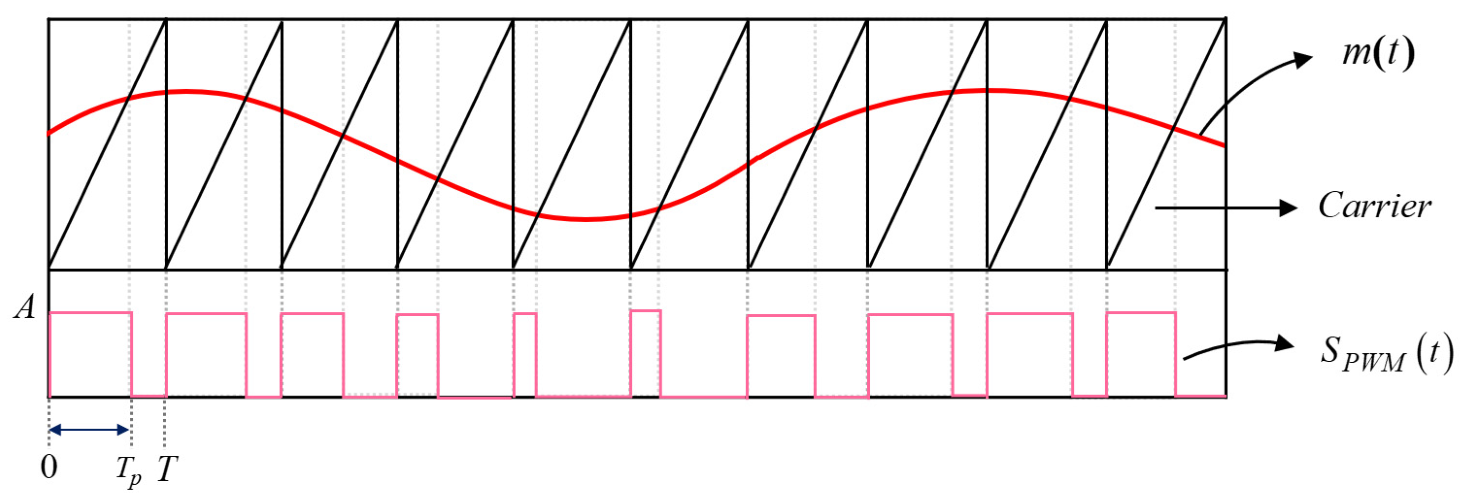
2.1. Analysis of Components in PWM Signals

PWM signal is represented by the S P W M ( t ) . PWM involves encoding information by varying the duration of the positive pulses within a square wave. The pulse width is directly proportional to the amplitude of the information signal. When the information signal exceeds the voltage of the sawtooth waveform, positive pulses are generated. Conversely, when the information signal is lower than the sawtooth waveform, negative pulses are produced. The relationship between the PWM signal and the sawtooth waveform is illustrated in Figure 1. It should also be noted that S P W M   ( t ) can interchangeably be expressed by ϕ P W M   ( t ) .
From Figure 1, the signal S P W M   ( t ) over a single period can be expressed by Equation (1), where A denotes the amplitude of the PWM signal. The variables t 0 and T p represent the initial time reference (usually set to 0) and the pulse width duration, respectively, while T determines the period of the PWM signal. This expression is then analyzed to determine the components of the signal using the Fourier series, where F 0 and F n denote the fundamental frequency and n -th harmonic frequency. Both are calculated using Equations (2) and (3), respectively, where the latter is expressed in a complex form, with j indicating the imaginary part. Later, for the complex form, j indicates the imaginary part.
S P W M t = A ; t 0 t t 0 + T p           0 ; t 0 + T p t   t 0 + T
F 0 = 1 T t 0 t 0 + T S P W M t d t = 1 T 0 T p A d t + T p T 0 d t = A T p T ,   w h e r e   t 0 = 0
F n = 1 T t 0 t 0 + T S P W M t · e j n ω 0 t d t = 1 T 0 T p A · e j n ω 0 t d t + T p T 0 · e j n ω 0 t d t       = A T j n ω 0 e j n ω 0 T p 1 ,   w h e r e   t 0 = 0
Subsequently, S P W M   ( t ) is re-expressed in terms of the Fourier series using F 0 and F n , yielding the PWM signal as shown in Equation (4). By substituting ω 0 = 2 π T , where ω 0 represents the angular fundamental frequency, into Equation (4) and rearranging, the original S P W M   ( t ) from Equation (1) is re-expressed as Equation (5). This re-expression, written in Equation (5), represents a summation of sinusoidal components.
S P W M t = F 0 + n = F n e j n ω 0 t                 = A T p T + n = 1 2 A T n ω 0 sin n ω 0 ( t T p ) + 2 A T n ω 0 sin n ω 0 t  
S P W M t = A T p T + n = 2 A T n 2 π T sin n ω 0 ( t T p ) + 2 A T n 2 π T sin n ω 0 t                 = A k p m ( t ) T + n = 1 A n π sin n ω 0 ( t k p m ( t ) ) + A n π sin n ω 0 t  
From Equation (5), the pulse width T p is proportional to the information signal m t , given by T p = k p m t T . The proportionality factor k p defines modulation depth in PWM, determining how m t influences pulse duration. It is observed that the PWM signal, S P W M   ( t ) , consists of a lowest frequency term, which is the information signal. In addition, it includes higher frequency terms, corresponding to phase modulation with a sine wave at various frequencies.

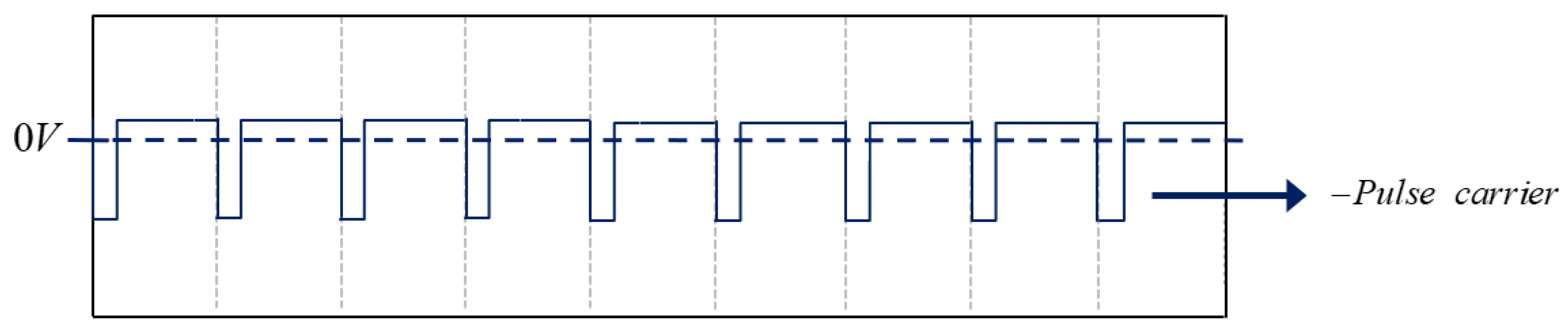
2.2. Analysis of Components in PPM Signals

For the analysis of PPM, we present an indirect approach, demonstrating that PPM arises from PWM with and without delay. The PPM signal is obtained by subtracting the delayed PWM signal, where the delay equals the width of the positive pulse, from the original PWM signal. The equation representing the components of the delayed PWM signal, where ε denotes the time delay, is derived from Equation (5). The delayed signal, S P W M D   t or S P W M   t ε , is expressed in Equation (6), where k p retains the same definition as in Equation (5).
S P W M D t = A k p m ( t ε ) T + n = 1 A n π sin n ω 0 ( t ε ) A n π sin n ω 0 ( t ε k p m ( t ε ) )
After obtaining the delayed PWM signal shown in Equation (6), the PWM signal without delay, as expressed in Equation (5), is first subtracted by the delayed PWM signal. The resulting expression is then rearranged, giving rise to Equation (7). As can be observed in Equation (7), the third term represents the pulse carrier signal, with the positive pulse width equal to ε .
ϕ P W M t ε ϕ P W M t = A k p m t m t ε T + n = 1 A n π sin n ω 0 t k p m t sin n ω 0 t ε k p m t ε n = 1 A n π sin n ω 0 t sin n ω 0 t ε
The subtraction process of the PWM signals with and without delay is illustrated in Figure 2. The first row of signal displays ϕ P W M   t , while the second row shows ϕ P W M   t ε . The third row illustrates the subtraction of the two upper signals, where the positive portion represents the PPM signal, ϕ P P M   t , and the negative portion corresponds to the pulse carrier signal. Finally, the last row shows the resulting output, which produces the PPM signal, ϕ P P M t .
Therefore, to isolate only the PPM modulation terms, the pulse carrier component is discarded. This pulse carrier term, illustrated in Figure 3, corresponds to a DC term that represents its duty cycle. In this context, the DC term is defined as D .
To ensure that the PPM signal maintains a low voltage level of 0 volts and a high pulse level of 1 volt (or any positive value), the DC component D of the pulse carrier term must be compensated. The resulting equation for the PPM signal is given in Equation (8).
ϕ P P M t = A k p m t m t ε T + n = 1 A n π sin n ω 0 t k p m t sin n ω 0 t ε k p m t ε + D
The term m t m ( t ε ) T in Equation (8), when compared with the period T , can be approximated as the derivative of the information signal ( d m t d t ). Based on this approximation, the equation for the components of the PPM signal, excluding the rectangular pulse carrier, is ultimately expressed in Equation (9).
ϕ P P M t = A k p d m t d t + n = 1 A n π sin n ω 0 t k p m t sin n ω 0 t ε k p m t ε + D
From Equation (9), it is shown that the components of the PPM signal consist of a low-frequency term, which is the direct current, and the information that has been differentiated. Meanwhile, the high-frequency components consist of the phase-modulated terms, which are the delayed and non-delayed versions subtracted from each other.

3. Proposed Techniques of Demodulation and Modulation

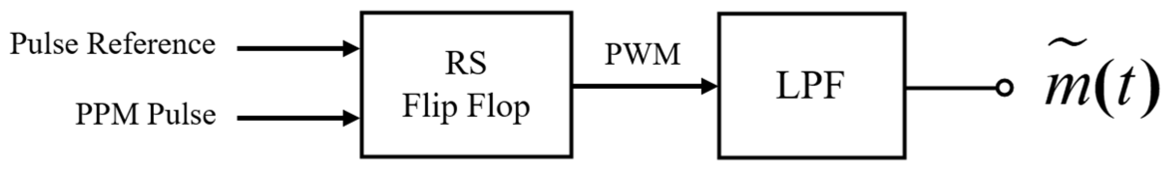
3.1. General PPM Demodulation

PPM demodulation generally involves converting PPM back into PWM, which requires a reference clock pulse signal and the PPM pulse as inputs to an RS Flip-Flop. Once the PWM signal is recovered, it is passed through a Low Pass Filter (LPF) to obtain the recovered information signal, m   ~ ( t ) . The block diagram of the demodulation process is shown in Figure 4.

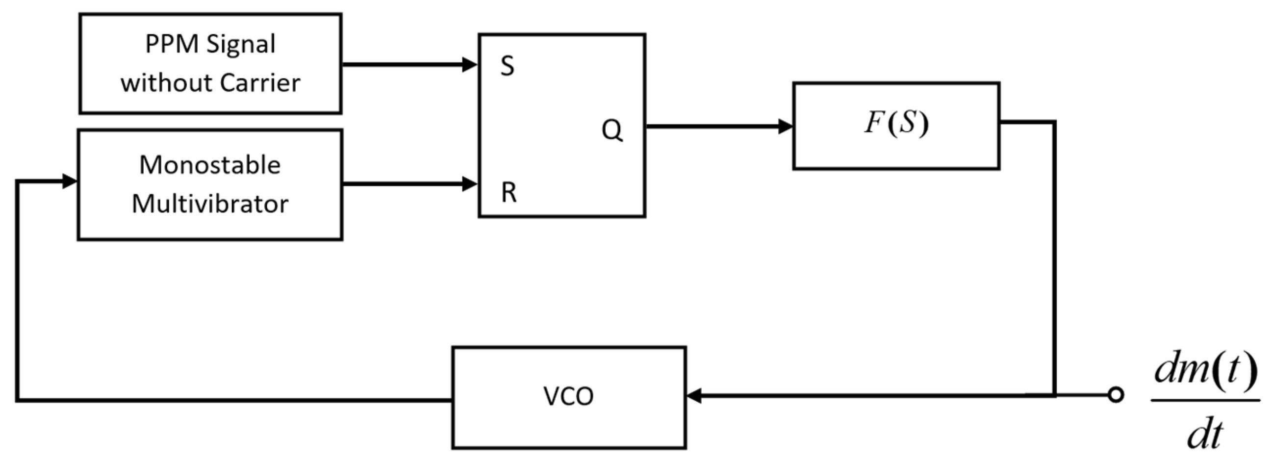
3.2. Proposed Carrierless PPM Techniques

The following sections analyze several classical carrierless PPM demodulation methods. Despite their different implementations—whether based on integration, PLL, or quasi-FM-PWM conversion—each approach consistently reveals that the demodulated output is fundamentally the derivative of the original message signal. Recognizing this common outcome motivates the development of a new modulation technique, presented in the subsequent section, which explicitly differentiates the message signal prior to PPM generation to simplify the overall system structure.

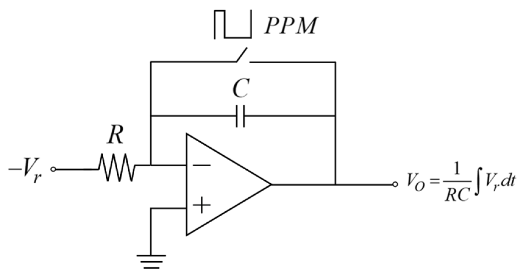
3.2.1. Demodulation via Integration: Derivative Recovery from PPM

PPM demodulation offers two options: converting PPM to PWM or converting PPM to PAM and then passing it through an LPF. Based on the analysis of the PPM signal without a carrier shown in Figure 5, the time interval ( t n ) between the n -th pulse and the previous pulse ( n 1 ) is analyzed. The relationship between these time intervals is then expressed in Equation (10), where m   ( t n ) equals to m   ( t n ) m   ( t n 1 ) after rearranging.
t n = n T + m t n n 1 T + m t n 1 = T + m t n
Hence, when the PPM signal controls the switch in an integrator circuit shown in Figure 6, the switch opens when the signal is LOW, causing the integrator to operate. When the signal is HIGH, the output of the integrator is set to 0. In this circuit, V r serves as a constant reference voltage, providing a fixed baseline for comparison. The output voltage, V o , is obtained through the mathematical method of integration and is given by Equation (11). The integration process is governed by the resistor R and capacitor C , where their values determine the rate of voltage accumulation over time.
V o = 1 R C n 1 T + m ( t n 1 ) n T + m t n V r d t = V r R C t n 1 T + m t n 1 n T + m t n     = V r R C n T + m t n n 1 T + m ( t n 1 )  
As shown in Equation (11), the terms in parentheses are like the ones presented in Equation (10) so Equation (11) is rewritten as Equation (12). Considering the term m   t n in relation to time T in Equation (12), the relationship for V o is expressed as in Equation (13) where the term m t n T appears. This term can be approximated as the derivative of the information signal m ( t ) with respect to time t .
V o = V r R C T + m t n
V o = V r × T R C 1 + m t n T V r × T R C + V r × T R C · d m t t
From Equation (13), V o represents the peak value of the sawtooth signal generated by the integration, as shown in Figure 7. When considering Equation (13), it can be observed that the result of the integration varies with the derivative of the information signal. Therefore, the demodulation process described above produces an output that is the derivative of the information signal, m ( t ) . To recover the original information signal, m ~   ( t ) , the value of V o from Equation (13) must be passed through a High-Pass Filter (HPF), and integration is required to recover the original information signal. This is because the DC term, when integrated, increases linearly. Thus, we can design the HPF in conjunction with the integrator to form a Band-Pass Filter (BPF). The low-frequency response of the BPF behaves like an HPF, while the high-frequency response behaves like an LPF, which is analogous to the behavior of the integrator.
This analysis demonstrates that the integration-based demodulation of carrierless PPM fundamentally produces the derivative of the original message signal. This recurring outcome suggests that differentiating the message signal prior to modulation could simplify the overall system.

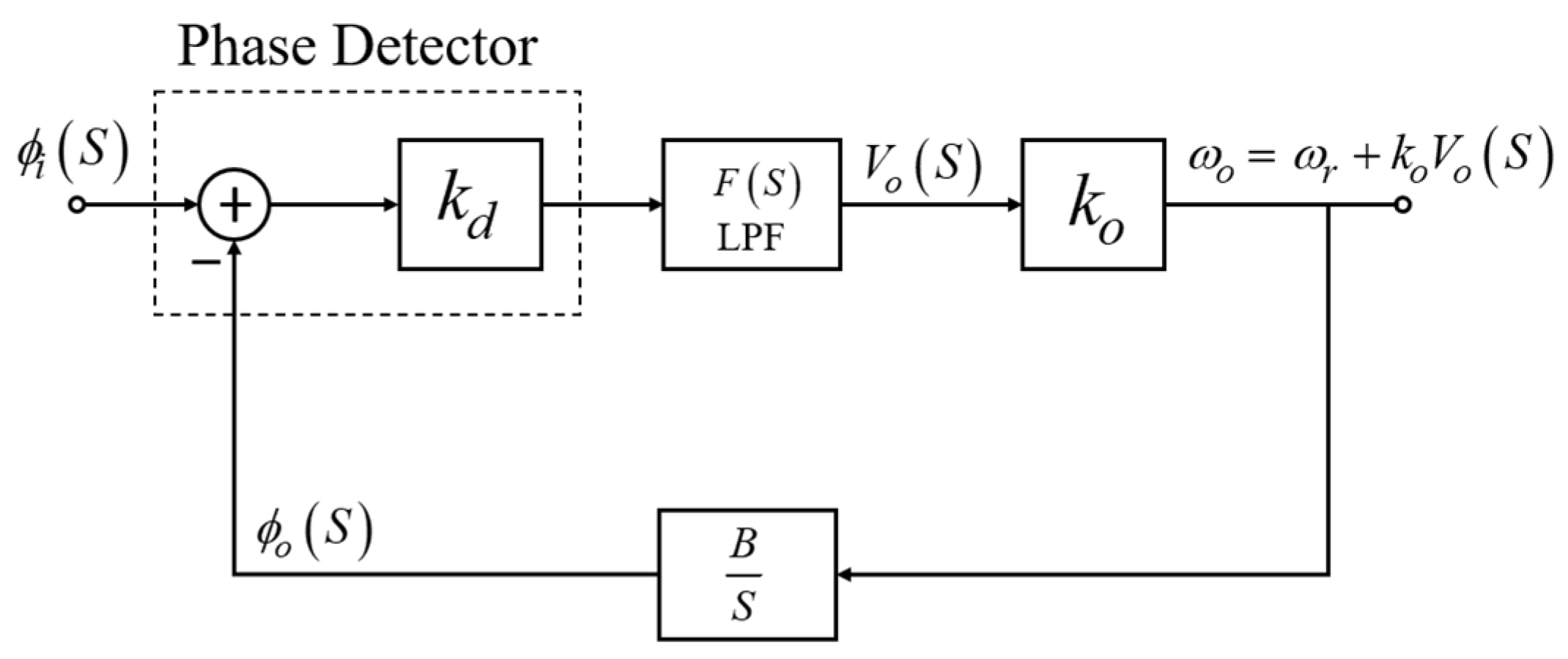
3.2.2. Demodulation via PLL: Phase-to-Derivative Relationship

For PPM demodulation using a PLL approach, the PPM signal is used as an input to the PLL circuit. The block diagram of the demodulation process is shown in Figure 8. In this approach, an RS flip-flop and a monostable multivibrator are used as a phase detector and the rest of the structure is abided by the conventional PLL structure.
To recover the information signal through the PPM demodulation process without the carrier using PLL, a conventional structure of PLL illustrated in Figure 9 is analyzed.
To elaborate the traditional block diagram of the PLL approach, key variables shown in Figure 9 are detailed as follows:
  • ϕ i ( S ) represents the Laplace transform of the phase input ϕ i   ( t ) ,
  • ϕ o ( S ) represents the Laplace transform of the phase output ϕ o   ( t ) ,
  • V o ( S ) represents the Laplace transform of the LPF output V o   ( t ) ,
  • ω r represents the Laplace transformation of a constant of free response,
  • ω L represents the cutoff frequency of the LPF,
  • F ( S ) refers to the transfer function of the LPF,
  • k b is a constant of a phase detection circuit,
  • k o is a constant of VCO sensitivity, and
  • B is a gain of an integrator circuit.
Referring to Figure 9, let us consider the points V o   ( S ) and ϕ o   ( S ) . The corresponding relationships are expressed in Equations (14) and (15), respectively.
V o ( S ) = F ( S ) k b ( ϕ i S ϕ o ( S ) )
ϕ o ( S ) = B S ω r + k o V o ( S )
Substituting Equation (15) into Equation (14) yields Equation (16) and later Equation (16) is adjusted, giving rise to Equation (17).
V o ( S ) = F ( S ) k b ϕ i S B S ω r + k o V o ( S )
V o ( S ) = F ( S ) k b ϕ i S B S ω r F ( S ) k b B S k o V o ( S ) F ( S ) k b
Translating the term B S k o V o ( S ) F ( S ) k b to the left-hand side (LHS) produces Equation (18). In the same equation, F ( S ) is defined as a first-order passive LHF, where its transfer function is expressed by ω L S + ω L and plugged into Equation (18), producing Equation (19).
V o S + B S k o V o ( S ) F ( S ) k b = F ( S ) k b ϕ i S B S ω r F ( S ) k b
V o S + B S k o V o ( S ) ω L S + ω L k b = ω L S + ω L k b ϕ i S B S ω r ω L S + ω L k b
After that, Equation (19) is rearranged, as shown in Equation (20). Once Equation (20) is obtained, the denominator, S ( S + ω L ) , is multiplied throughout Equation (20), resulting in Equation (21) with a slight rearrangement.
V o S + B ω L S ( S + ω L ) k o V o ( S ) k b = ω L S + ω L k b ϕ i S B ω L S ( S + ω L ) ω r k b
S 2 V o S + S ω L V o S + B ω L k o V o ( S ) k b = S ω L k b ϕ i S B ω L ω r k b
To facilitate the solution for the response, the inverse Laplace transform of Equation (21) is applied, resulting in Equation (22).
d 2 V o t d t 2 + ω L d V o t d t + B ω L k o V o ( t ) k b = ω L k b d ϕ i t t B ω L ω r k b
It is assumed that the PLL is a stable system that has reached a steady state. Consequently, the solution for the forced response is determined by setting ϕ i t = ω i t + θ i and substituting this expression into Equation (22), resulting in Equation (23).
d 2 V o t d t 2 + ω L d V o t d t + B ω L k o V o ( t ) k b = ω L k b ω i B ω L ω r k b
When the forcing function on the right-hand side of the equation is constant, the first and second derivatives of the assumed solution are equal to zero (according to the undetermined coefficient method). Thus, Equation (23) can be rewritten as Equation (24) and Equation (24) is reformulated as Equation (25).
B ω L k o V o ( t ) k b = ω L k b ω i B ω L ω r k b
V o ( t ) = k b ω i B k b ω r / B k b k o
For the sake of convenience in analyzing, let B be 1, and Equation (25) is simplified as shown in Equation (26). When considering the PPM signal equation as phase modulation, where ϕ i t is proportional to m t , the frequency term ω i in Equation (26) can be expressed as the derivative of ω i = d ϕ i t d t = d m ( t ) d t . Consequently, Equation (26) can be rewritten as Equation (27).
V o ( t ) = ω i ω r / k o
V o ( t ) = d m ( t ) d t ω r / k o
Finally, it is evident that the output voltage of the LPF in Equation (27), which is a component of the PLL, is the derivative of the transmitted message signal.
Thus, the PLL-based demodulation approach also confirms that the demodulated output is the derivative of the message signal. This further supports the idea of applying differentiation before modulation to streamline the process.

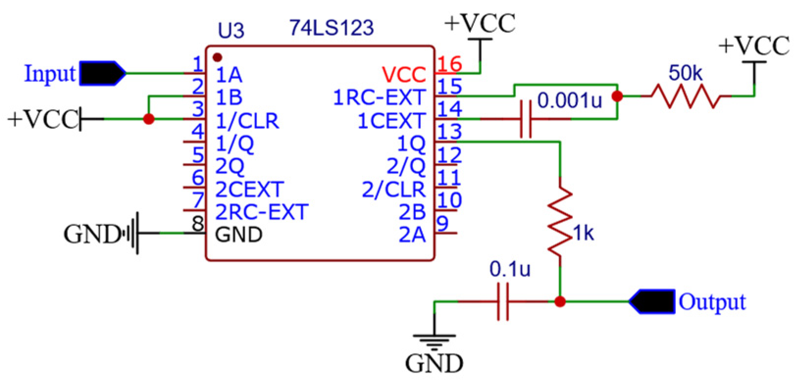
3.2.3. Demodulation via Quasi-FM-PWM: Frequency Modulation Perspective

The analysis of demodulating PPM signals without a carrier using a PLL reveals that, by nature, the PLL circuit is an FM demodulator or a phase demodulator where the information signal is differentiated. Consequently, we conclude that carrierless PPM can be considered a form of frequency modulation, where the information signal is differentiated. This offers an alternative perspective on the matter. Furthermore, in the research conducted by Rapeepong et al. [19], they proposed an FM demodulation technique by converting the information signal into a quasi-FM-PWM signal. Their analysis demonstrated that a quasi-FM-PWM signal contains low-frequency components that vary with frequency, which in turn also varies with the information signal, as expressed in Equation (28). In the same equation, A represents the amplitude and T i is the period of the information signal, m ( t ) . Additionally, k is a proportionality constant that influences the transformation of FM signals into quasi-FM-PWM signals. Based on their analysis, the quasi-FM-PWM signal is expressed as Equation (29), where the component of PWM signal is converted from FM signals by a monostable multivibrator circuit.
A T p T i = A T p k m ( t )
ϕ p w F M t = A T p T i + n = 1 A s i n ( n ω i t T p ) / n π + A s i n ( n ω i t ) / n π              
Plugging the expression in Equation (28) into Equation (29) leads to Equation (30), in which the information signal, m ( t ) , appears within the quasi-FM-PWM waveform.
ϕ p w F M t = A T p k m ( t ) + n = 1 A s i n ( n ω i t T p ) / n π + A s i n ( n ω i t ) / n π              
Therefore, in the case of a carrierless PPM signal, which is a form of phase modulation, if considered from the perspective of frequency modulation, it can be realized as frequency modulation where the information signal is differentiated. When it is converted into a quasi-FM-PWM signal using a monostable multivibrator, it yields its low-frequency term, which varies with the derivative of the information signal, as demonstrated by Equation (31) [19,23].
A T p T i = A T p k d m ( t ) d t
As a result, the PPM signal without a carrier can be demodulated by utilizing a monostable multivibrator, followed by passing its output through an LPF. This process produces an output that corresponds to the derivative of the information signal, with the rate of amplification being dependent on the pulse width of the monostable multivibrator. To retrieve the original message, the differentiated signal must be integrated. The block diagram of the system is shown in Figure 10.
The quasi-FM-PWM demodulation method likewise yields the derivative of the message signal as its output. This consistent finding across different demodulation techniques motivates the proposed approach of differentiating the message signal prior to PPM generation.

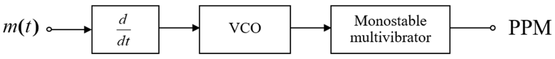
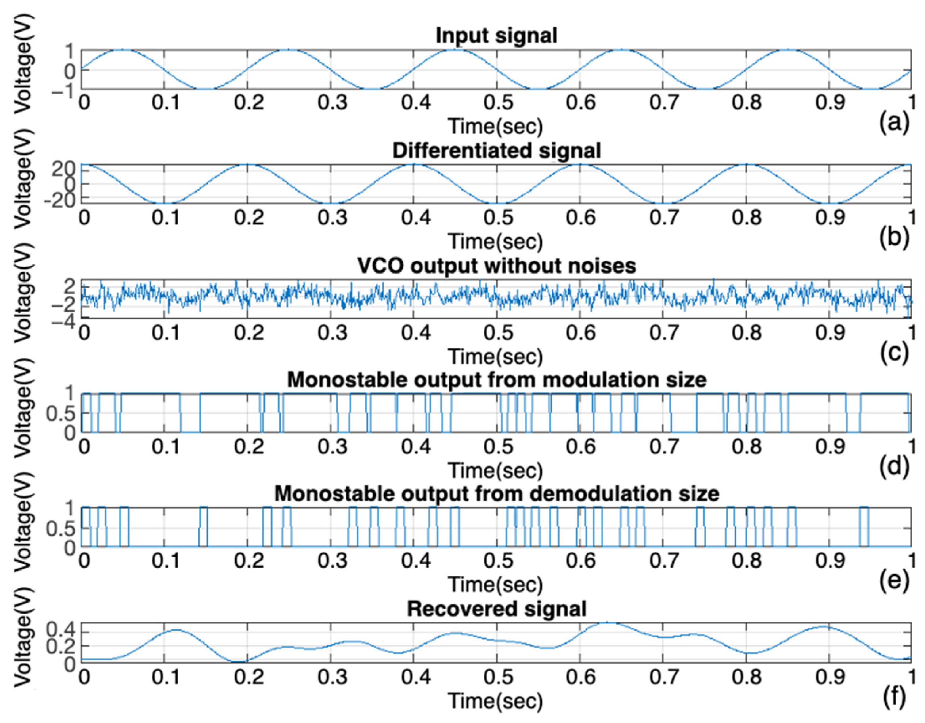
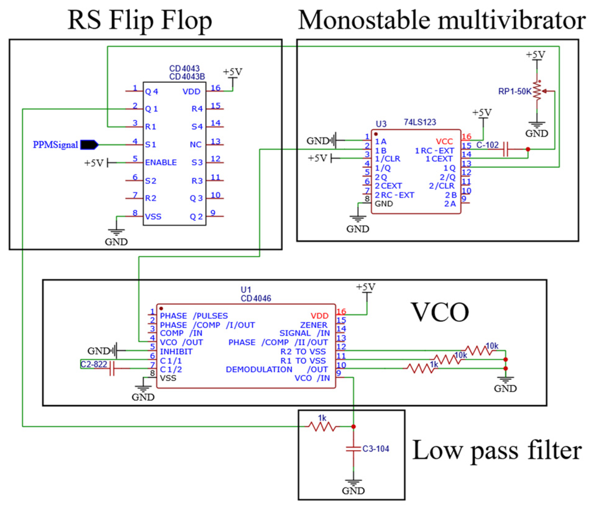
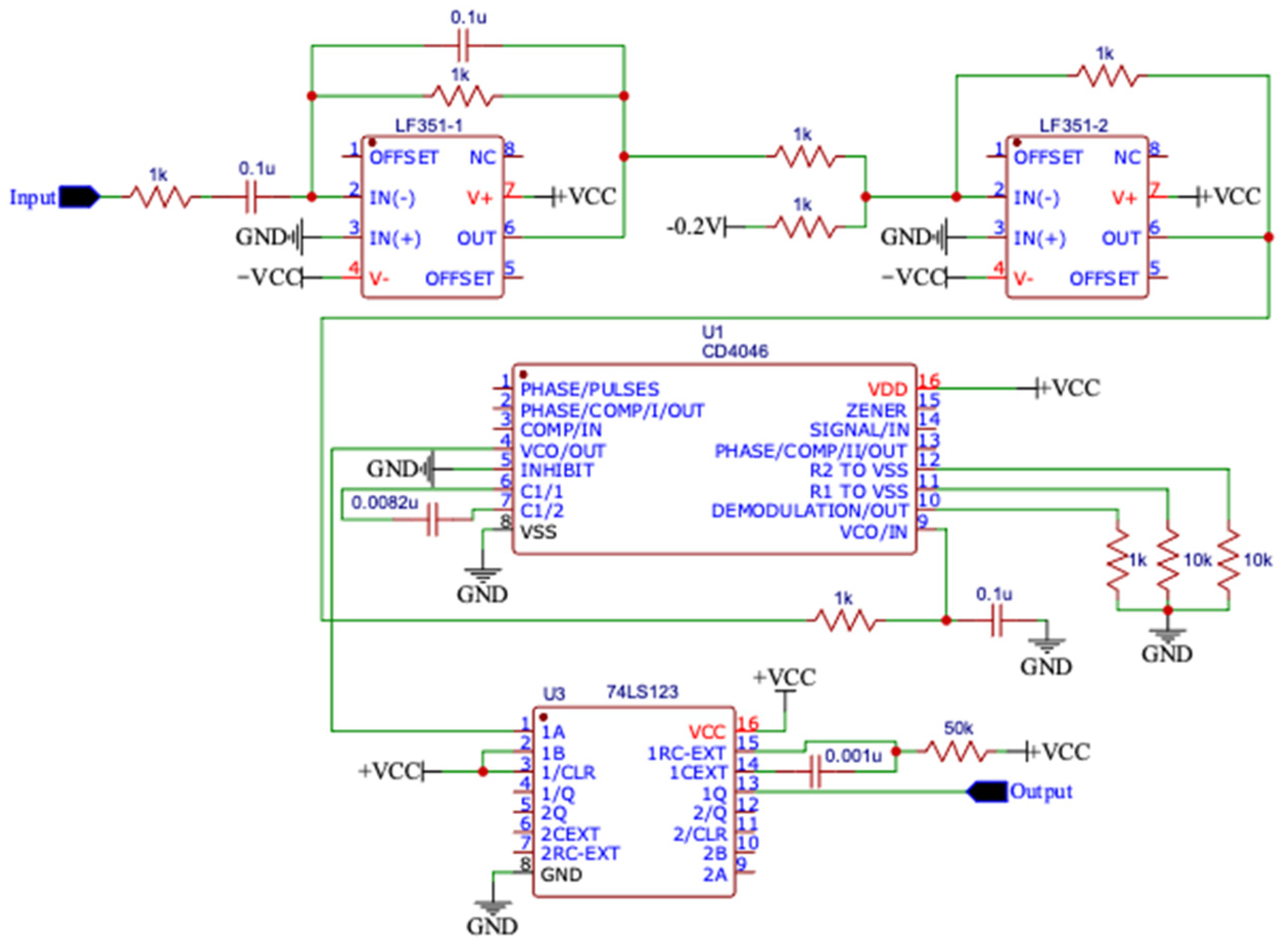
3.2.4. Proposed Derivative-Based PPM Modulation Using VCO and Monostable Multivibrator

Building on the previous analyses, which show that all major carrierless PPM demodulation methods yield the derivative of the message signal, we propose a novel modulation technique. Instead of generating PPM through conventional PWM comparison and monostable multivibrator circuits, this method first differentiates the message signal and then uses it to drive a voltage-controlled oscillator (VCO). The VCO output, representing a frequency-modulated signal, is then fed into a monostable multivibrator to generate the PPM signal. This approach leverages the fundamental relationship between phase, frequency, and pulse position modulation, and directly aligns the modulation process with the inherent properties revealed in demodulation. The block diagram of this simplified structure is shown in Figure 11. This method offers an efficient and structurally streamlined alternative for carrierless PPM generation.

4. Performance Analysis

The SNR analyses presented in Equations (38), (43), and (49) characterize the noise performance of the three demodulation methods under AWGN conditions for carrierless PPM signals. Since any practical PPM communication system requires one of these demodulation methods at the receiver, analyzing their individual performance characteristics provides essential insights into the overall system performance limits. These analyses are relevant to the proposed derivative-based modulation technique as follows. The demodulation methods examined—integration, PLL, and FM-PWM conversion—process the PPM pulse timing information regardless of the generation method used. Consequently, the fundamental noise conversion mechanisms from amplitude domain to time domain, as described in Equations (33)–(36), apply to PPM signals generated through our proposed VCO–monostable multivibrator approach.
The variables in this section retain the same definitions as those previously established. As these demodulation methods respond to pulse timing and amplitude characteristics rather than the modulation generation process, the derived SNR expressions remain applicable to the proposed system. However, the VCO and monostable multivibrator components may introduce their own noise contributions that are not captured in the current analysis. Therefore, while Equations (38), (43), and (49) provide a theoretical framework for understanding the demodulation performance, a complete SNR analysis of the proposed system would require additional consideration of these factors.

4.1. Error Analysis of Demodulation Using Integration

For the analysis of error values in demodulation using integration, we begin by comparing the PPM signal with added noise to recover the original PPM signal. When the PPM signal, combined with noise, is subjected to comparison through zero crossing detection, the output from the comparison is obtained, as depicted in Figure 12.
To illustrate the transmission of noise in the spatial domain to the time–domain noise, we consider the probability density function (PDF) of additive white Gaussian noise (AWGN), as shown in Equation (32). In Equation (32), the variance of AWGN denotes σ n 2 and n represents noise. When a noise signal is added to the PPM signal and subjected to signal comparison at any reference level, or even at a reference level of 0 (zero crossing), the result will be similar. The magnitude–domain interference that is converted to time–domain interference varies with the signal slope, where a higher slope results in less interference, as illustrated in Figure 12.
f ( n ) = 1 / 2 π σ n 2 e n 2 2 σ n 2
Following this, let s be the signal slope of the PPM signal, expressed by v t , where v denotes the PPM voltage signal and t represents time. Given this, the relationship of the interference transitioning from magnitude–domain interference to time–domain interference can be expressed by Equation (33). After that, Equation (32) is recast using the relationship in Equation (33), producing Equation (34).
t = v / s     v = n = s t
f ( t ) = 1 / 2 π σ n 2 e s t 2 2 σ n 2
When the time-shifted PPM signal without a carrier is used to control the integrator with a reference voltage input of V r , it influences the initial condition of n o . Consequently, the expression for n o , representing the magnitude of AWGN output, is formulated in Equation (35). With this initial condition, the PDF of n o , which is a noise output, is acquired and mathematically stated in Equation (36).
0 t V r d t = V r t = n o   t = n o / V r
f n o = 1 / 2 π σ n 2 e s n o V r 2 / 2 σ n 2 = 1 / 2 π σ n 2 e n o 2 / 2 σ n 2 V r 2 s 2
By calculating the power output from Equation (36), the power of the noise signal n o at the output of the integrator during demodulation is thus equal to N o V r 2 S 2 . From the perspective of PPM as a narrow rectangular positive pulse phase modulation, the maximum variation angle is less than 2 π k p m ( t ) , where k p is the modulation index and m ( t ) is the information signal. If the information signal is fully demodulated, the message signal power S m is obtained, as expressed by Equation (37), where a low-pass bandwidth B L is used along with the low-pass bandwidth B L , and the noise signal is attenuated to B L N o V r 2 S 2
S m = k p 2 m 2 ( t ) ¯
Once the power of both the information and filter noise signals is acquired, the signal-to-noise ratio is then calculated and presented in Equation (38).
S m N = k p 2 m 2 t ¯ / B L N o V r 2 S 2 = k p 2 S 2 V r 2 m 2 t ¯ B L N o  

4.2. PLL Error Analysis

Under the scenario where the phase detector is digital (RS flip-flop), the PPM input signal passing through the channel is first sent to a comparator. Consequently, the power of the time–domain noise signal is equivalent to that in integrator demodulation. When considering the transfer function at the point where the output is the derivative of the information signal, after the LPF component of the PLL, the transfer function becomes a BPF, as expressed by Equation (39).
H ( S ) = S ω L k b ϕ i ( S ) S 2 V o S + S ω L V o S + B ω L k b k o V o ( S )
If the bandwidth of this BPF is set to B P F , the noise power at the output of the LPF can be determined by transforming the time–domain noise into angle–domain noise, resulting in the following expression in Equation (40). When substituting the time–domain and angle–domain relationships into Equation (40), the PDF of AWGN in forms of the angle–domain noise is obtained in Equation (41).
θ = 2 π t / T
f ( θ ) = 1 / 2 π σ n 2 e s θ T 2 / 2 σ n 2 2 π 2
For simplicity, N o replaces 2 σ n 2 . In the same manner as the previous calculation of noise power, the phase noise power is given by N θ = N o 2 π 2 / S T 2 . After passing through the BPF with the bandwidth B P F , the noise power output, N B P , is attenuated and is expressed by Equation (42).
N B P = N o 2 π 2 S 2 T 2 H S 2 = N o 2 π 2 S 2 T 2 B P F
By using the same information signal mentioned previously, the signal-to-noise ratio in terms of power is given by Equation (43).
S m N B P = k p 2 m 2 t ¯ / N o 2 π 2 S 2 T 2 B P F = k p 2 S 2 T 2 2 π 2 m 2 t ¯ N o B P F

4.3. FM-PWM Error Analysis

Under the same assumptions as the signal-to-noise analysis for both the integrator control and PLL previously, the PPM signal contaminated with noise is first compared. This comparison results in a time error t , which in turn causes a frequency disturbance f , where the relationship is defined by Equation (44).
± f = 1 T ± t 1 T = t T ( T ± t )
Under the condition that T is very much greater than t ( T t ), f is approximated by Equation (45). Then, the PDF of AWGN in terms of the frequency–domain noise is generated in Equation (46), where Equation (45) is slightly adjusted to be t f T 2 .
f t / T 2
f ( f ) = 1 / 2 π σ n 2 e s f T 2 2 / 2 σ n 2
Subsequently, Equation (28), adapted from Rapeepong et al. [19], is rewritten in terms of frequency expression aligned with Equation (45) and rearranged, as shown by Equation (47). This is done to obtain the term of noise signal n o . At the same time, the information signal m ( t ) is superseded by the noise signal n o .
A T p T i = A T p k n 0 A T p f = A T p k n 0 f = k n 0
After determining the relationship of the noise signal n o , the PDF of AGWN in this quasi-FM-PWM approach is derived by substituting n o into Equation (46), resulting in Equation (48). The power corresponding to Equation (48) is computed, yielding N F M P W M = N o S T 2 k 2 .
f n 0 = 1 / 2 π σ n 2 e s T 2 k n o 2 / 2 σ n 2 = 1 / 2 π σ n 2 e n o 2 / N o s T 2 k 2
To gauge the effect of noise, the signal-to-noise ratio using the same PPM information signal in conjunction with this noise in terms of power is calculated and expressed by Equation (49).
S m N F M P W M = k p 2 m 2 t ¯ / N o S T 2 k 2 = S 2 T 4 k 3 k p 2 m 2 t ¯ N o

5. Experiments and Results

5.1. MATLAB Simulations

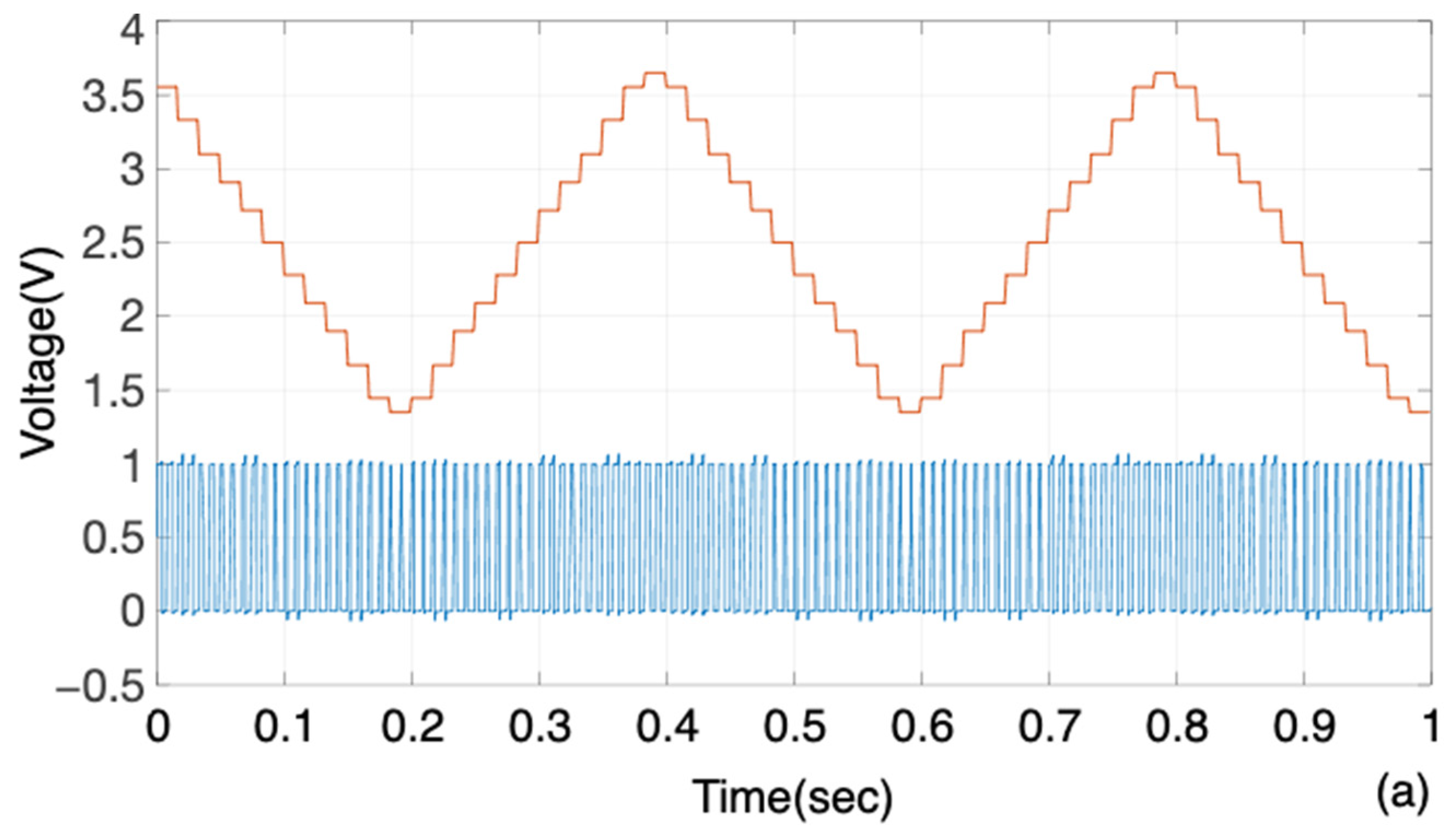
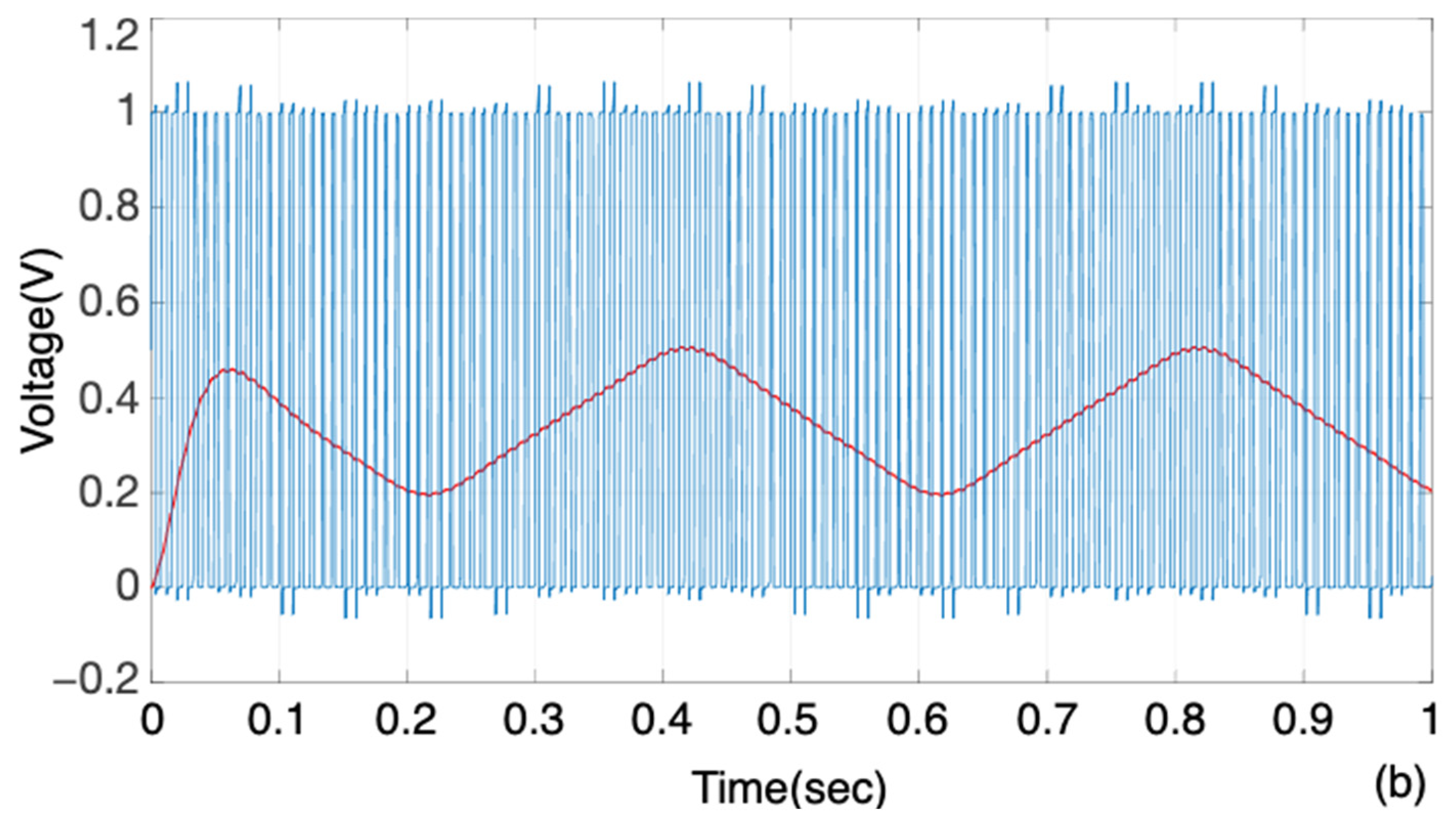
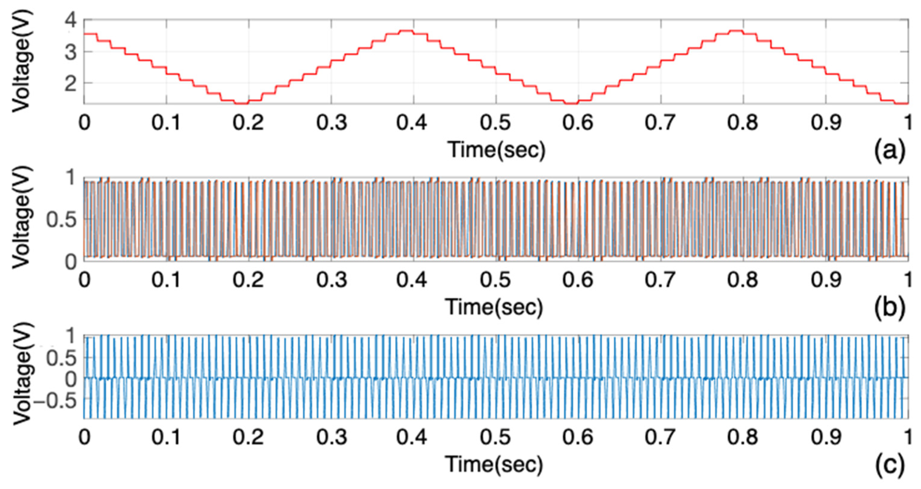
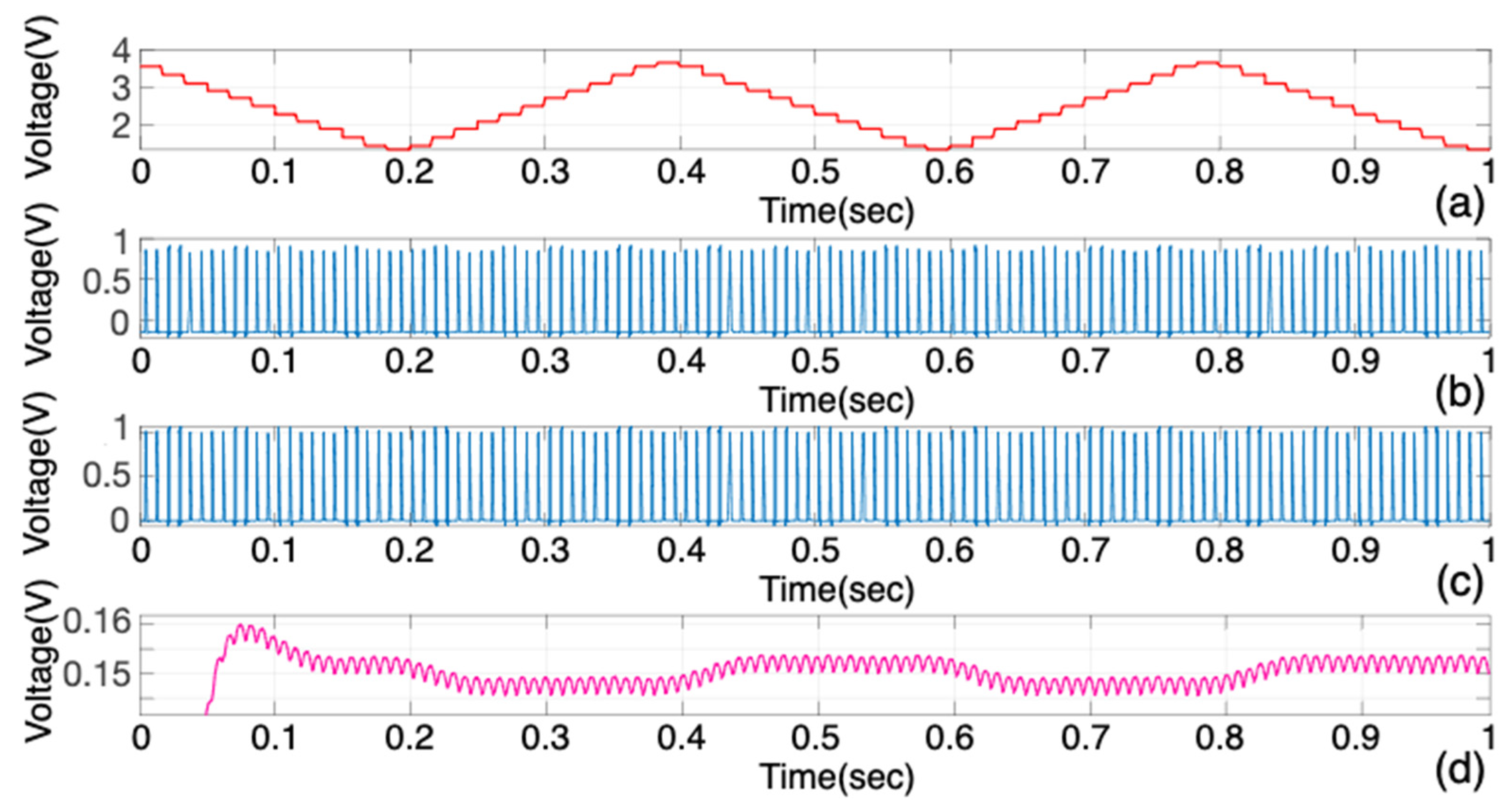
5.1.1. Syntheses of PWM and PPM Signals

To validate the analysis presented in the previous section, this section utilizes computer simulation via MATLAB under an academic license. The synthesis incorporates components of the PWM signal (see Equation (5)) and the PPM signal (see Equation (9)).
A.
PWM Signal Generation and Analysis
The PWM signal generation process utilizes a comparative approach where the input message signal is continuously compared against a reference sawtooth waveform. This fundamental technique produces a PWM output where the width of each individual pulse directly correlates with the instantaneous amplitude of the message signal at the sampling moment. This relationship ensures that the analog information content is accurately preserved within the digital pulse train format, enabling reliable signal transmission and subsequent recovery. The implementation code for this section can be found in Code S1 of the Supplementary Materials.
The synthesis results of the PWM signal components are demonstrated in Figure 13, which illustrates both the modulation process and the demodulation capability. The simulation reveals that the sampled-and-held information signal maintains a direct correspondence with the PWM pulse widths, while the demodulated output successfully reconstructs the original information signal with minimal distortion. This validates the effectiveness of PWM as a robust modulation technique for analog signal processing applications.
B.
PPM Signal Synthesis Through Signal Processing
Building upon the PWM foundation, the PPM signal synthesis employs sophisticated mathematical operations to convert width-modulated information into position-modulated pulses. The synthesis process involves the strategic manipulation of delayed and non-delayed PWM signals, where the temporal relationship between these components determines the final PPM characteristics. The implementation code for this section can be found in Code S2 of the Supplementary Materials.
Figure 14 presents the comprehensive results of this synthesis approach, demonstrating the subtraction process between delayed and non-delayed PWM signals. The simulation results reveal a critical insight: as higher harmonic components are incorporated into the synthesis process, the resulting PPM signal increasingly approaches the ideal theoretical response. This observation highlights the importance of harmonic content in achieving optimal PPM signal quality and suggests that bandwidth considerations play a crucial role in practical PPM system design.
C.
Signal Conditioning and Final Processing
The final stage of PPM signal processing requires careful signal conditioning to ensure optimal performance characteristics. This involves the systematic removal of reference pulse components that could introduce interference or bias into the demodulation process. Additionally, the introduction of appropriate DC offset compensation ensures proper signal level management throughout the processing chain. The implementation code for this section can be found in Code S3 of the Supplementary Materials.
Figure 15 illustrates the complete signal conditioning process and its effectiveness in producing a clean, de-modulable PPM signal. The results demonstrate successful reference pulse subtraction and DC offset addition, culminating in accurate signal recovery that closely matches the original information content. This multi-stage processing approach validates the practical feasibility of PPM implementation in real-world communication systems.
D.
Implementation Methodology
The MATLAB implementation provides straightforward visualization and analysis capabilities for both modulation techniques without requiring complex coding structures or extensive signal processing operations. This approach enables clear observation of the modulation processes, facilitating both educational understanding and practical system development. The simulation results confirm that both PWM and PPM techniques offer reliable methods for information encoding, transmission, and recovery, with each method providing distinct advantages depending on the specific application requirements and system constraints.

5.1.2. Noise Resistance Analysis

Building upon the fundamental PWM and PPM synthesis demonstrated in the previous section, this section addresses the critical practical consideration of noise immunity through comparative MATLAB simulation. The analysis specifically examines the robustness of the proposed derivative-based PPM technique when subjected to various noise conditions, providing quantitative assessment of system performance degradation. The implementation code for this section can be found in Code S4 of the Supplementary Materials.
A.
Experimental Configuration and Methodology
The experimental setup employs a derivative-based PPM generation system utilizing a voltage-controlled oscillator (VCO) with a monostable multivibrator for modulation. The VCO represents the most noise-susceptible component due to inherent capacitive and inductive characteristics, making it the logical injection point for noise analysis. The system parameters were standardized with a 5-Hz sinusoidal input signal at 1 Vpp amplitude, while the VCO operated at a base frequency of 20 Hz with frequency sensitivity of 1 Hz per volt. Both the modulation and demodulation monostable multivibrators employed identical threshold settings of 0.5 V for consistent comparison.
The demodulation process utilizes the Quasi-FM-PWM technique described in Section 3.2.3, selected for its implementation simplicity and computational efficiency. The demodulation chain consists of a monostable multivibrator followed by a sixth-order Butterworth low-pass filter with an 8 Hz cutoff frequency, providing adequate selectivity while maintaining signal integrity.
B.
Noise-free Performance Analysis
Figure 16 demonstrates the complete PPM generation and demodulation chain under ideal noise-free conditions. The signal processing sequence begins with the original input signal (first trace) and its mathematical derivative (second trace), which serves as the control input for frequency modulation. The VCO output (third trace) exhibits clear frequency variations corresponding to the derivative amplitude, while the monostable output (fourth trace) produces the desired PPM signal with position-modulated pulses.
The demodulation process, illustrated in traces five and six, shows successful signal recovery through the Quasi-FM-PWM technique. The monostable processing of the received PPM signal (fifth trace) and subsequent filtering produces a demodulated output (sixth trace) that closely matches the original input signal, demonstrating effective signal reconstruction under optimal conditions.
C.
Noise Impact Assessment
Figure 17 presents identical processing under realistic noise conditions, where additive noise is introduced at the VCO stage to simulate practical implementation challenges. The comparison reveals observable degradation in signal quality throughout the processing chain, with noise propagation affecting both the PPM generation accuracy and demodulation fidelity. Despite the presence of noise, the fundamental PPM structure remains recognizable, indicating inherent robustness of the position-modulation approach.
D.
Quantitative Performance Evaluation
Table 2 provides comprehensive quantitative analysis of system performance across varying SNR conditions using Pearson correlation coefficients as the primary metric for signal fidelity assessment. The correlation values compare the recovered signal with the differentiated input signal, as the demodulation process inherently recovers the derivative rather than the original input signal. The negative correlation coefficients, ranging from −0.1505 under severe noise conditions (SNR = −8.4387 dB) to −0.8908 under noise-free conditions, indicate that the recovered signal exhibits a phase shift relative to the differentiated signal while maintaining strong correlation magnitude, demonstrating successful derivative signal recovery.
The data reveals that the system maintains reasonable performance even under challenging noise conditions, with correlation coefficients improving systematically as SNR increases. Notably, at SNR = 6.1815 dB, the correlation coefficient reaches −0.8802, approaching the noise-free performance level of −0.8908, indicating effective noise tolerance within practical operating ranges.

5.2. Experiment of Carrierless PPM Demodulation Using an Integration Method

For the demodulation of carrierless PPM signals, the methods of integration, PLL, and conversion to quasi-FM-PWM have been implemented using hardware circuits. For the integration method, the circuit shown in Figure 6 is implemented. In the experiment, a 12 kHz PPM carrier was used with input signals of a 180 Hz sine wave and a 180 Hz triangle wave as the information signals. The demodulation results are manifested in Figure 18.

5.3. Experiment of Carrierless PPM Demodulation Using a PLL Method

For demodulation using PLL, a PPM carrier frequency of 12 kHz is utilized with a lock range of 9.6 kHz to 14.1 kHz. The circuit is portrayed in Figure 19. The input information signals are sine and triangle waves of the same frequency as those used for integrator demodulation. These signals are first modulated into PPM and then demodulated using the proposed methods. The demodulation results are shown in Figure 20.

5.4. Experiment of Carrierless PPM Demodulation Using Conversion to Quasi-FM-PWM Signal

For the experiment involving the demodulation of PPM signals without a carrier by converting them into a quasi-FM-PWM signal, a monostable circuit and an RC lowpass filter are used, as shown in Figure 21. For this experiment, PPM modulation without a carrier under the same conditions is experimented like those conducted for the first two demodulation methods. The experimental results are shown in Figure 22.

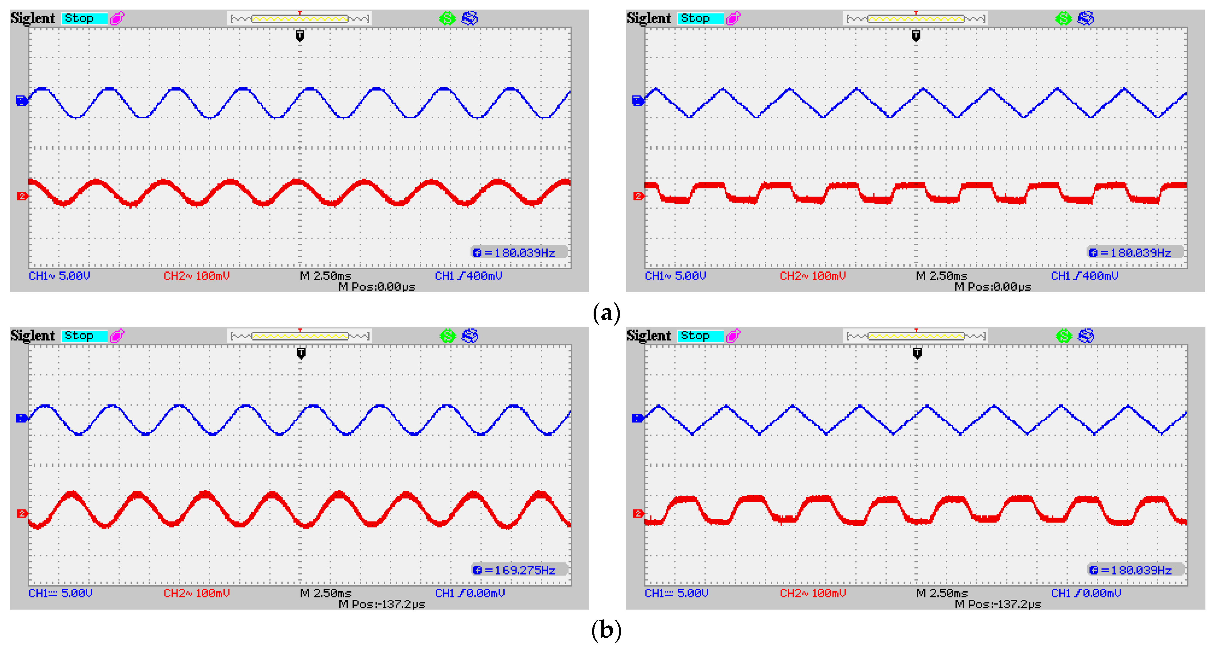
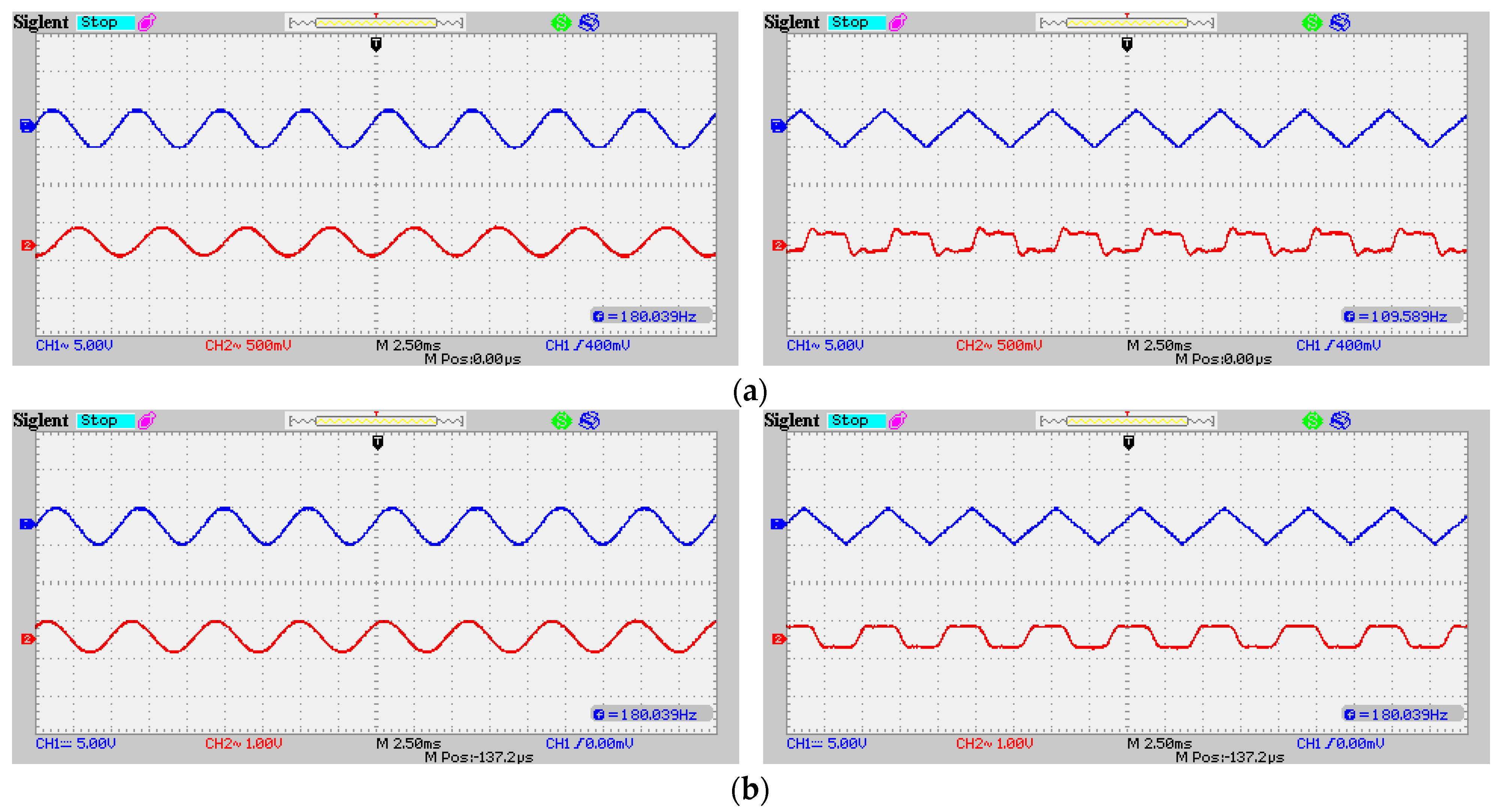
5.5. Experiment of Proposed Novel Derivative-Based PPM Modulation Using VCO and Monostable Multivibrator

For the novel method of generating PPM without a carrier, a differentiator circuit created using an operational amplifier is employed. The VCO utilizes the IC4046, and the 74LS123 is used as the monostable multivibrator. The circuit diagram is shown in Figure 23. The experimental results demonstrate a comparison between the traditional method, which uses a sawtooth wave compared with the information signal and feeds to the monostable circuit, and the novel proposed method. The comparison is shown in both the time domain and frequency domain, as illustrated in Figure 24.

6. Discussion and Analysis of Results

6.1. Non-Ideal Component Analysis

The theoretical analysis presented in previous sections assumes ideal component behavior. This section examines the impact of practical limitations on system performance through MATLAB (MATLAB Version R2024b Update 5 (24.2.0.2871072)) simulation incorporating non-ideal characteristics of the differentiator, VCO, and monostable multivibrator. The simulation code for Section 6.1.1 and Section 6.1.2 can be found in Code S5 of the Supplementary Materials.

6.1.1. Practical Limitations of System Components

The simulation employs a 5 Hz sinusoidal input signal sampled at 1 kHz over 1 s duration, maintaining consistency with the experimental parameters used in Section 5.1.2. The 1 kHz sampling frequency provides adequate oversampling (200:1 ratio) to capture system dynamics while remaining computationally efficient. Non-ideal parameters are selected to represent realistic component tolerances: differentiator noise factor of 0.1 reflects typical operational amplifier noise characteristics; VCO phase noise standard deviation of 0.05 radians corresponds to moderate-quality oscillator specifications; and timing jitter values of 0.001 s (VCO) and 0.002 s (monostable) represent achievable precision with standard integrated circuits. The VCO center frequency of 20 Hz with 1 Hz/V sensitivity ensures adequate frequency deviation range while maintaining linear operation, and the 10 ms monostable pulse duration provides sufficient resolution for PPM pulse positioning analysis.
A.
Differentiator Noise Amplification
The differentiator circuit exhibits inherent high-frequency noise amplification due to its frequency-proportional gain characteristic. Simulation results demonstrate significant noise amplification, with measured values of 196.52 dB for a 5 Hz input signal. The differentiator output SNR degrades to −13.06 dB, indicating substantial noise injection into the signal path. An examination of various signal frequencies demonstrates performance degradation that depends on frequency. At 1 Hz, noise amplification reaches 26.80 dB, whereas at 50 Hz, it decreases to −7.24 dB. This dependency on frequency significantly affects the suitability of the differentiator for different message signal bandwidths, with lower frequencies undergoing more pronounced noise amplification.
B.
VCO Phase Noise and Timing Jitter
VCO implementation introduces two primary non-idealities: phase noise and timing jitter. Simulation results show phase noise RMS of 1.1903 radians and timing jitter standard deviation of 1.0 ms. These impairments degrade the VCO output SNR to −2.87 dB, representing significant performance degradation from ideal conditions. Phase noise manifests as random variations in the VCO output phase, while timing jitter affects the precision of pulse positioning in the PPM signal. The combined effect reduces overall system correlation from the ideal case, with measured performance showing substantial deviation from theoretical predictions.
C.
Monostable Multivibrator Timing Inaccuracies
The monostable multivibrator exhibits timing inaccuracies characterized by ±2.0 ms standard deviation for a nominal 10.0 ms pulse duration. This represents 20% relative timing accuracy, significantly affecting PPM pulse positioning precision. These variations introduce systematic errors in the pulse position modulation process, degrading demodulation accuracy. Temperature effects, component aging, and supply voltage variations contribute additional timing uncertainties not captured in the current simulation model. These factors would further degrade system performance in practical implementations.
D.
System-Level Performance Impact
Combined non-ideal effects result in substantial system performance degradation. The overall system SNR measures −2.88 dB, with Pearson correlation coefficient of −0.1276 for the non-ideal system compared to −0.4028 for the ideal case. This represents a correlation loss of 0.2752, indicating significant signal fidelity reduction.

6.1.2. Message Signal Bandwidth and Slew Rate Limitations

A.
Differentiator Frequency Response Limitations
The performance of the differentiator varies significantly depending on the characteristics of the input signal. To ensure effective operation, the signal bandwidth should be restricted to less than fs/10 (100 Hz for a 1 kHz sampling rate), allowing noise levels to remain within acceptable limits. When signals exceed this bandwidth, they undergo severe noise amplification, which can overpower the desired signal content. Slew rate limitations become apparent for high-frequency or rapidly changing signals. The maximum recommended input signal slew rate is 100 V/s to prevent differentiator saturation and maintain linear operation. Signals with higher slew rates experience nonlinear distortion and increased noise sensitivity.
B.
Signal Frequency Dependencies
Simulation analysis across test frequencies (1, 5, 10, 20, 50 Hz) reveals optimal performance in the low-frequency range. Signal frequencies below 20 Hz maintain reasonable SNR performance, while frequencies above 50 Hz show improved noise characteristics but may approach system bandwidth limitations. The maximum derivative amplitude varies proportionally with frequency, reaching 309.02 for 50 Hz signals compared to 6.28 for 1 Hz signals. This scaling affects VCO sensitivity requirements and system dynamic range considerations.

6.2. Discussion and Perspectives

6.2.1. Interpretation of Results

The experimental validation demonstrates successful implementation of both conventional and proposed derivative-based PPM modulation techniques across multiple demodulation approaches. The MATLAB simulations and hardware implementations provide comprehensive evidence for the feasibility of carrierless PPM systems in practical communication applications.
A.
Signal Synthesis and Modulation Performance
The MATLAB simulations confirm that both PWM and PPM signals can be synthesized effectively using mathematical operations on delayed and non-delayed signal components. The PWM generation demonstrates direct correlation between message signal amplitude and pulse width, maintaining analog information integrity within the digital pulse train format. The PPM synthesis through differential processing of PWM signals successfully converts width-modulated information to position-modulated pulses, with signal quality improving as higher harmonic components are incorporated.
The derivative-based PPM approach demonstrates favorable performance in the tested conditions, as evidenced by the VCO-based implementation. The frequency modulation of the VCO output based on the differentiated input signal produces clear position-modulated pulses, validating the theoretical foundation presented in Section 3.2.1.
B.
Demodulation Method Comparison
Three demodulation techniques were evaluated: integration, PLL, and quasi-FM-PWM conversion. Each method successfully recovered the original information signals from both conventional and proposed PPM formats:
  • Integration Method: Demonstrated effective signal recovery for both sinusoidal and triangular waveforms, with the integrator circuit providing consistent demodulation performance across different signal types.
  • PLL Method: Operating with a 12 kHz carrier frequency and 9.6–14.1 kHz lock range, the PLL successfully tracked frequency variations and recovered the modulating signals with acceptable fidelity.
  • Quasi-FM-PWM Conversion: The monostable multivibrator approach with RC low-pass filtering showed robust performance, particularly suitable for applications requiring implementation simplicity.
C.
Noise Resistance Analysis
The quantitative noise analysis reveals important characteristics of the proposed system. Under noise-free conditions, the Pearson correlation coefficient of −0.8908 indicates strong signal recovery fidelity. The negative correlation values reflect the inherent phase relationship in derivative-based demodulation, where the recovered signal corresponds to the differentiated input rather than the original signal directly.
Performance degradation under noise conditions follows predictable patterns, with correlation coefficients ranging from −0.1505 at SNR = −8.44 dB to −0.8802 at SNR = 6.18 dB. The system maintains reasonable performance even under challenging noise conditions, demonstrating practical viability for real-world implementations.
D.
Clarification of Signal Recovery Characteristics
The experimental results demonstrate that all demodulation methods recover the derivative of the original message signal, representing the theoretically expected behavior of the proposed derivative-based PPM technique. This clarifies the conceptual framework and addresses signal recovery characteristics.
The negative Pearson correlation coefficients in Table 2 (−0.8908 to −0.1505) mathematically confirm that recovered signals correlate with the differentiated input signal, validating successful derivative-based implementation. Visual evidence in Figure 15, Figure 16, Figure 17, Figure 18, Figure 20, Figure 22, and Figure 24 shows consistent phase shifts characteristic of differentiation operations across all demodulation methods.
This derivative recovery provides system flexibility rather than limitation. Applications requiring the original signal can incorporate integration stages for signal reconstruction, while others can directly utilize derivative information for differential processing applications. The consistency across all three demodulation techniques confirms this characteristic is fundamental to the modulation approach, validating the robustness of the derivative-based PPM concept.
E.
Integration Circuit Implementation
The hardware experiments utilized simple test signals (sine, triangle, and square waves) with well-defined derivative relationships, allowing direct verification of the derivative recovery without requiring integration circuits. For sinusoidal inputs, the recovered cosine signals clearly demonstrate the expected 90° phase shift characteristic of differentiation. While integration circuits were not implemented in these experiments due to the predictable nature of the test waveforms, complex message signals would require an integration stage following demodulation to reconstruct the original signal from its recovered derivative. This approach maintains experimental clarity while acknowledging the integration requirement for practical applications involving arbitrary message signals.

6.2.2. Implications

The experimental work extends beyond basic MATLAB simulation of PWM signals to demonstrate a novel derivative-based PPM generation technique. While VCO and PLL implementations are established technologies, their application in derivative-based carrierless PPM represents a specific contribution to position modulation techniques. A key innovation is the practical use of a derivative-based framework to generate position-modulated pulses with reduced circuit complexity.
The comparative analysis between conventional and proposed methods provides quantitative evidence of system performance differences. The experimental validation using multiple demodulation approaches demonstrates the robustness and versatility of the proposed technique across different implementation scenarios.
A.
Laboratory-Scale Implementation Considerations
The experimental parameters (12 kHz PPM carrier, 180 Hz information signals) reflect laboratory-scale validation using available instrumentation and components. This approach follows established research methodology where proof-of-concept validation precedes system scaling. The frequency selection ensures adequate separation between carrier and information signal frequencies while remaining within the operational capabilities of the test equipment.
The principle demonstrated at these frequencies remains proportional when extended to higher frequencies suitable for optical wireless communication (OWC) applications. The fundamental mathematical relationships governing derivative-based PPM generation remain valid regardless of operating frequency, with implementation constraints determined by component specifications rather than theoretical limitations.
B.
System Performance Characteristics
The experimental results demonstrate several key performance characteristics:
1.
Modulation Fidelity: Both time–domain and frequency–domain analysis confirm accurate signal modulation and recovery across different signal types.
2.
Implementation Flexibility: Three distinct demodulation approaches validate system compatibility with various receiver architectures.
3.
Noise Tolerance: Quantitative analysis demonstrates acceptable performance degradation characteristics under realistic noise conditions.
4.
Circuit Simplicity: Hardware implementation using standard components (op-amps, VCO IC4046, monostable 74LS123) demonstrates practical feasibility without requiring specialized or expensive components.
C.
Design Simplification Rationale
Compared to typical carrierless PPM systems, the proposed architecture adopts a simplified structure in several specific aspects. First, it reduces the number of active components by not requiring phase-locked loops, carrier recovery circuits, or digital synchronization elements such as flip-flops. Second, the design relies on RC-defined time constants and VCO bias control for modulation and demodulation, which can reduce tuning complexity compared to systems involving loop filter design or digital clock recovery. Third, the implementation uses analog building blocks and does not depend on digital platforms or FPGA-based logic, which may offer practical benefits in scenarios where a compact circuit layout, ease of implementation, or minimal digital infrastructure is preferred.

6.2.3. Limitations

A.
Frequency Range Constraints
The experimental validation was conducted at laboratory-scale frequencies (12 kHz carrier, 180 Hz information signals) due to equipment limitations. While the theoretical framework scales to higher frequencies, practical implementation at OWC-relevant frequencies requires validation with appropriate high-frequency components and measurement systems.
B.
Component Performance Dependencies
The VCO-based implementation exhibits inherent sensitivity to component variations and environmental factors. Temperature stability, supply voltage fluctuations, and component aging can affect frequency accuracy and system performance. The noise analysis focused on additive noise but did not comprehensively address systematic errors introduced by component non-linearities.
C.
Demodulation Phase Relationships
The derivative-based approach inherently recovers the differentiated signal rather than the original information signal. While this characteristic was quantified through correlation analysis, practical applications may require additional signal processing to reconstruct the original waveform, potentially introducing complexity and processing delays.
D.
Power Consumption Analysis Gap
The current work does not provide quantitative power consumption analysis. While the circuit simplicity may suggest potential power efficiency advantages, comparative power measurements against alternative PPM generation techniques remain to be conducted.

6.2.4. Future Directions

A.
High-Frequency Implementation and OWC Integration
Future work should aim to extend the demonstrated principles to frequencies suitable for OWC systems by advancing circuit design and system integration. This includes the development and validation of high-frequency VCO circuits for efficient LED modulation in the MHz range, optimization of component selection and circuit performance for high-speed operation, and the integration of LED driver circuits with comprehensive optical channel characterization.
B.
Comprehensive Power Analysis
Quantitative power consumption analysis is necessary to substantiate the claimed efficiency advantages. This should include comparative power measurements between conventional and proposed PPM generation techniques, incorporating other state-of-the-art methods, as well as an evaluation of power consumption across varying modulation depths and signal frequencies. Furthermore, strategies for optimizing power usage in battery-operated OWC applications should be developed to enhance system efficiency.
C.
Advanced Signal Processing Integration
Enhancing signal processing capabilities could help overcome existing limitations. This includes implementing adaptive filtering techniques to improve noise resistance, developing automatic gain control systems to mitigate component variations, and exploring digital signal processing methods to enhance accuracy and flexibility.
D.
System-Level Performance Evaluation
A comprehensive system evaluation should encompass end-to-end testing with LED transmitters and photodetector receivers, comparative analysis of modulation techniques regarding bandwidth efficiency, implementation complexity, and power consumption, as well as bit error rate (BER) assessment under varying channel conditions. Moreover, simulation-based evaluation using MATLAB (MATLAB Version R2024b Update 5 (24.2.0.2871072)) should be conducted to benchmark SNR, jitter tolerance, and signal fidelity relative to conventional carrierless PPM systems.
E.
Practical Implementation Optimization
Further development should focus on practical deployment considerations, including temperature compensation techniques to enhance stability, circuit miniaturization and integration for improved feasibility, and cost analysis to assess manufacturability for commercial applications.
These future directions provide a clear pathway for advancing the demonstrated laboratory-scale proof-of-concept toward practical OWC system implementation while addressing the limitations identified in the current work.

7. Conclusions

This work introduces a simplified carrierless pulse position modulation (PPM) technique based on differentiating the input signal prior to modulation. The proposed system comprises a differentiator, voltage-controlled oscillator (VCO), and monostable multivibrator to form a compact analog transmitter that generates a PPM waveform without requiring a carrier or synchronization reference. This structure was motivated by the observation that existing carrierless PPM demodulators—whether based on integration, PLLs, or quasi-FM-PWM methods—consistently yield the derivative of the transmitted message.
Theoretical analysis demonstrated that PPM inherently encodes the derivative of the signal under various processing schemes. Building on this, the proposed modulation method intentionally differentiates the message signal at the outset, streamlining the architecture by aligning modulation and demodulation characteristics. The signal path and behavior were validated through MATLAB (MATLAB Version R2024b Update 5 (24.2.0.2871072)) simulations and hardware-level circuit experiments. In all tested demodulation configurations, the recovered signals closely match the time-derivative of the input message, as confirmed by waveform comparison and correlation metrics.
The integration of the output to retrieve the original message was not performed in this study to ensure alignment with the objective of demonstrating the simplified derivative-based modulation scheme. This approach also aimed to confirm the consistent recovery of the signal derivative across multiple demodulation methods. Signal-to-noise ratio (SNR) analyses for the three demodulator types are presented and shown to be applicable to the proposed system. The influence of non-ideal hardware characteristics—such as VCO jitter, differentiator noise amplification, and monostable timing drift—is discussed qualitatively.
Future work will focus on integrating full message recovery, modeling hardware non-idealities, and benchmarking the system against conventional carrierless PPM approaches.

Supplementary Materials

We have five codes for the Supplementary Materials which can be downloaded at: https://www.mdpi.com/article/10.3390/app15116272/s1, Code S1: PWM Signal Generation and Analysis for Section 5.1.1.(A), Code S2: PPM Signal Synthesis Through Signal Processing for Section 5.1.1.(B), Code S3: Signal Conditioning and Final Processing for Section 5.1.1.(C), Code S4: Noise Resistance Analysis for Section 5.1.2., Code S5: Simulation for Non Ideal Analysis and Bandwidth as well as Slew Rate for Section 6.1.

Author Contributions

Conceptualization, J.K., P.W., A.S., and P.T.; data curation, C.K.-i.; methodology, J.K., P.W., C.K.-i., and P.T.; formal analysis, J.K., P.W., A.S., and P.T.; investigation, A.S. and C.K.-i.; software, C.K.-i.; resources, C.K.-i.; validation, J.K., A.S., and P.T.; visualization, C.K.-i., writing—original draft, J.K., P.W., A.S., C.K.-i. and P.T.; writing—review and editing, J.K., P.W., A.S., and P.T.; supervision, J.K. and P.W.; Funding acquisition, P.W. All authors have read and agreed to the published version of the manuscript.

Funding

This work was financially supported by King Mongkut’s Institute of Technology Ladkrabang through the Research Fund under Grant Number KREF016727.

Institutional Review Board Statement

Not applicable.

Informed Consent Statement

Not applicable.

Data Availability Statement

Data is contained within the article or Supplementary Materials.

Acknowledgments

The authors express their gratitude to King Mongkut’s Institute of Technology Ladkrabang for providing facility support.

Conflicts of Interest

The authors declare no conflicts of interest. The authors also declare that they have no known competing financial interests or personal relationships that could have appeared to influence the work reported in this paper.

References

  1. Sarelius, D. FMS flight simulator encoder: Practice without crashing your models. Elektor-Electron. 2004, 30, 22–27. [Google Scholar]
  2. Wisartpong, P.; Koseeyaporn, J.; Wardkein, P. Pulse position modulation based on phase locked loop. In Proceedings of the 2009 6th International Conference on Electrical Engineering/Electronics, Computer, Telecommunications and Information Technology, Pattaya, Thailand, 6–9 May 2009; pp. 578–581. [Google Scholar]
  3. Wilson, B.; Ghassemlooy, Z. Pulse time modulation techniques for optical communications: A review. IEE Proc. J. Optoelectron. 1993, 140, 346–358. [Google Scholar] [CrossRef]
  4. Park, H.; Barry, J.R. Modulation analysis for wireless infrared communications. In Proceedings of the IEEE International Conference on Communications ICC ‘95, Seattle, WA, USA, 18–22 June 1995; pp. 1182–1186. [Google Scholar]
  5. Al-Gailani, S.A.; Salleh, M.F.M.; Salem, A.A.; Shaddad, R.Q.; Sheikh, U.U.; Algeelani, N.A. A survey of free space optics (fso) communication systems, links, and networks. IEEE Access 2021, 9, 7353–7373. [Google Scholar] [CrossRef]
  6. Tang, W.; Wang, S.; Xu, Y.; Yu, Z. The research process, application, and the future development of pulse-position modulation. J. Phys. Conf. Ser. 2022, 2384, 012026. [Google Scholar] [CrossRef]
  7. Yu, Z. Application of digital pulse position modulation. In Proceedings of the International Conference on Neural Networks, Information, and Communication Engineering (NNICE 2022), Qingdao, China, 25–27 March 2022. [Google Scholar]
  8. Mahdiraji, G.A.; Zahedi, E. Comparison of selected digital modulation schemes (ook, ppm and dpim) for wireless optical communications. In Proceedings of the 2006 4th Student Conference on Research and Development, Shah Alam, Malaysia, 27–28 June 2006; pp. 5–10. [Google Scholar]
  9. Liu, Y. Design of pulse position modulation system based on programmable logic device. In Proceedings of the International Conference on Neural Networks, Information, and Communication Engineering (NNICE 2022), Qingdao, China, 25–27 March 2022. [Google Scholar]
  10. Li, B. Design of digital pulse-position modulation system based on minimum distance method. In Proceedings of the International Conference on Neural Networks, Information, and Communication Engineering (NNICE 2022), Qingdao, China, 25–27 March 2022. [Google Scholar]
  11. Gopal, P.; Jain, V.K.; Kar, S. Spectral analysis of intensity modulation schemes in free space optical communications. IET Commun. 2015, 9, 909–916. [Google Scholar] [CrossRef]
  12. Gu, S.; Liang, C.; Zhang, J. Spectral analysis of (multi-) pulse-position modulation. J. Phys. Conf. Ser. 2021, 2093, 012024. [Google Scholar] [CrossRef]
  13. Ebrahimi, F.; Ghassemlooy, Z.; Olyaee, S. Investigation of a hybrid ofdm-pwm/ppm visible light communications system. Opt. Commun. 2018, 429, 65–71. [Google Scholar] [CrossRef]
  14. Xu, Y.; Chen, Z.; Gong, Z.; Xia, Z.; Yuan, T.; Gu, Z.; Zhao, W.; Chen, J. Hybrid modulation scheme for visible light communi-cation using cmos. Opt. Commun. 2019, 440, 89–94. [Google Scholar] [CrossRef]
  15. Carlson, A.B.; Crilly, P.B. Communication Systems: An Introduction to Signals and Noise in Electrical Communication, 5th ed.; McGraw-Hill: New York City, NY, USA, 2010; pp. 275–279. [Google Scholar]
  16. Chiang, H.H. Electronic Wave Forming and Processing Circuits; Wiley: Hoboken, NJ, USA, 1986. [Google Scholar]
  17. Lathi, B.P.; Ding, Z. Modern Digital and Analog Communication, 5th ed.; Oxford University Press: Oxford, UK, 2018. [Google Scholar]
  18. Furihata, M. FM Detector Using Monostable Multivibrators. US4504792A, 12 March 1985. [Google Scholar]
  19. Boongsri, R.; Wardkein, P.; Chodkaveekityada, P. FM demodulation based on fm to pwm conversion with voltage gain con-trol. In Proceedings of the International Conference on Computer, Networks and Communication Engineering (ICCNCE 2013), Beijing, China, 23–24 May 2013; pp. 140–143. [Google Scholar]
  20. Safyannikov, N.M.; Bureneva, O. Time-to-voltage converters based on the time-sharing principle. IEEE Access 2020, 8, 17442–17453. [Google Scholar] [CrossRef]
  21. Shin, S.; Jung, Y.; Kweon, S.-J.; Lee, E.; Park, J.-H.; Kim, J.; Yoo, H.-J.; Je, M. Design of reconfigurable time-to-digital converter based on cascaded time interpolators for electrical impedance spectroscopy. Sensors 2020, 20, 1889. [Google Scholar] [CrossRef] [PubMed]
  22. Crepaldi, M.; Casu, M.R.; Graziano, M.; Zamboni, M. A mixed-signal demodulator for a low-complexity ir-uwb receiver: Methodology, simulation and design. Integration 2009, 42, 47–60. [Google Scholar] [CrossRef]
  23. Haykin, S.; Moher, M. Communication Systems, 5th ed.; John Wiley & Sons, Inc: Hoboken, NJ, USA, 2009. [Google Scholar]
  24. Kozawa, Y. Selective multi-pulse pulse position modulation for lighting constrained visible light communications. In Proceedings of the 2024 IEEE International Symposium on Circuits and Systems (ISCAS), Singapore, 19–22 May 2024. [Google Scholar]
  25. Li, M.; Zhang, B.; Zhang, B.; Liu, W.; Kim, T.; Wang, W.; Zhao, X.; Wang, C. Multi-carrier based positional modulation design with discrete phase values for metasurface elements. Digit. Signal Process. 2023, 137, 104047. [Google Scholar] [CrossRef]
  26. Bamiedakis, N.; Penty, R.V.; White, I.H. Carrierless amplitude and phase modulation in wireless visible light communication systems. Philos. Trans. R. Soc. A 2020, 378, 20190181. [Google Scholar] [CrossRef] [PubMed]
  27. Pulkkinen, M.; Haapala, T.; Salomaa, J.; Halonen, K. Low-power wireless transceiver with 67-nW differential pulse-position modulation transmitter. IEEE Trans. Circuits Syst. I Regul. Pap. 2020, 67, 5468–5481. [Google Scholar] [CrossRef]
  28. Khani, H. Improved detection schemes for non-coherent pulse-position modulation. Wirel. Pers. Commun. 2023, 131, 2173–2192. [Google Scholar] [CrossRef] [PubMed]
  29. Elsayed, E.E.; Yousif, B.B. Performance enhancement of M-ary pulse-position modulation for a wavelength division multi-plexing free-space optical systems impaired by interchannel crosstalk, pointing error, and ase noise. Opt. Commun. 2020, 475, 126219. [Google Scholar] [CrossRef]
  30. Kim, J.; Clerckx, B. Wireless information and power transfer for iot: Pulse position modulation, integrated receiver, and ex-perimental validation. IEEE Internet Things J. 2022, 9, 12378–12394. [Google Scholar] [CrossRef]
Figure 1. Comparison between the information signal and the sawtooth waveform (carrier) yields the output S P W M   ( t ) .
Applsci 15 06272 g001
Figure 2. Subtraction of delayed and non-delayed PWM signals, resulting in the PPM signal.
Applsci 15 06272 g002
Figure 3. Pulse carrier signal obtained from the third term of Equation (7).
Applsci 15 06272 g003
Figure 4. A block diagram of general PPM demodulation.
Applsci 15 06272 g004
Figure 5. Analysis of the carrierless PPM signal, focusing on the time interval ( t n ) between consecutive pulses.
Applsci 15 06272 g005
Figure 6. Integrator circuit controlled by the PPM signal through the switch.
Applsci 15 06272 g006
Figure 7. An illustration of the relationship between the integration process and the resulting V o , where the black dashed line represents the approximated signal derived from Equation (13), the red line denotes the integrator circuit output, and the navy-blue line corresponds to the PPM signal.
Applsci 15 06272 g007
Figure 8. Block diagram of the PLL used for PPM demodulation.
Applsci 15 06272 g008
Figure 9. Conventional block diagram of the PLL approach.
Applsci 15 06272 g009
Figure 10. Demodulating PPM from the perspective of FM modulation, in conjunction with its conversion to PWM. Derived with permission from Ref [19].
Applsci 15 06272 g010
Figure 11. Novel derivative-based PPM modulation using VCO and monostable multivibrator.
Applsci 15 06272 g011
Figure 12. Comparison of the noise signal added to the PPM signals, where v is the PPM voltage signal, and t represents time. (a) Low slope input, and (b) High slope input.
Applsci 15 06272 g012
Figure 13. MATLAB simulation results demonstrating PWM signal generation and demodulation performance. (a) Comparison between the original information signal (smooth curve) and the generated PWM signal (pulse train), showing the direct relationship between signal amplitude and pulse width; (b) PWM signal input and successfully demodulated output signal, demonstrating effective signal recovery with minimal distortion.
Applsci 15 06272 g013aApplsci 15 06272 g013b
Figure 14. PPM signal synthesis through mathematical manipulation of PWM signals. (a) Original information signal serving as the modulation reference; (b) Delayed PWM signal (dashed) and non-delayed PWM signal (solid) used for differential processing; (c) Resulting PPM signal obtained by subtracting the delayed PWM from the non-delayed PWM, effectively converting pulse width information to pulse position information.
Applsci 15 06272 g014
Figure 15. Complete PPM signal processing chain with conditioning and demodulation. (a) Original information signal for reference comparison; (b) PPM signal after reference pulse subtraction; (c) PPM signal with reference pulse removed and DC offset added; (d) Successfully demodulated output signal demonstrating accurate information recovery through the complete PPM processing chain.
Applsci 15 06272 g015
Figure 16. PPM generation and demodulation performance under noise-free conditions. (a) Input sinusoidal signal (5 Hz, 1 Vpp); (b) Differentiated input signal serving as VCO control; (c) VCO output with frequency modulation based on derivative amplitude; (d) PPM signal generated by monostable multivibrator processing of VCO output; (e) Demodulated signal after monostable processing of received PPM; (f) Final recovered signal following low-pass filtering, representing the reconstructed derivative of the original input.
Applsci 15 06272 g016
Figure 17. PPM generation and demodulation performance with VCO noise injection. (a) Input sinusoidal signal (5 Hz, 1 Vpp); (b) Differentiated input signal serving as VCO control; (c) Noise-corrupted VCO output showing degraded frequency modulation characteristics; (d) PPM signal generated from noisy VCO output, exhibiting reduced position accuracy; (e) Demodulated signal after monostable processing showing noise-induced distortion; (f) Final recovered signal with noise-related degradation, demonstrating system performance under realistic operating conditions.
Applsci 15 06272 g017
Figure 18. Demodulation results using an integrator circuit: (a) Output of the integrator demodulation with a 180 Hz sine wave and triangle wave input from conventional PPM signal; (b) Output of the integrator demodulation with a 180 Hz sine wave and triangle wave input from proposed PPM signal. (CH1) Information signal (upper line); (CH2) Demodulated output signal using the integrator circuit (lower line).
Applsci 15 06272 g018
Figure 19. Carrierless demodulating circuit using the PLL technique.
Applsci 15 06272 g019
Figure 20. Demodulation results using the PLL circuit: (a) Output of the PLL demodulation with sine wave and triangle wave input from conventional PPM modulation signal; (b) Output of the PLL demodulation with sine wave and triangle wave input from proposed PPM modulation signal. (CH1) Information signal (upper line); (CH2) Demodulated output signal using the PLL circuit (lower line).
Applsci 15 06272 g020
Figure 21. Demodulation circuit for carrierless PPM using a monostable multivibrator circuit and an RC lowpass filter.
Applsci 15 06272 g021
Figure 22. Demodulation results using the approach of conversion to a quasi-FM-PWM signal: (a) Output of the quasi-FM and PWM demodulation with sine wave and triangle wave input from conventional PPM modulation signal; (b) Output of the quasi-FM and PWM demodulation with sine wave and triangle wave input from proposed PPM modulation signal. (CH1) Information signal (upper line); (CH2) Demodulated output signal using the monostable circuit and LPF (lower line).
Applsci 15 06272 g022
Figure 23. Novel proposed circuit for generating carrierless PPM using VCO.
Applsci 15 06272 g023
Figure 24. PPM modulating results: (a) Traditional technique, and (b) Novel proposed approach.
Applsci 15 06272 g024
Table 1. Summary of selected related works on PPM and their comparison to the proposed method.
Ref. No.Authors/Title (Year)Application/System ContextAdvantagesLimitationsComparison to Proposed Method
[2]Wisartpong et al. (2009) PLL-based analog PPM circuit with carrier/no-carrier optionsSimple tuning, compact implementationRequires PLL, RS flip-flop; medium complexityProposed system eliminates PLL and flip-flop, yielding lower complexity and fewer analog blocks
[6]Tang et al. (2022) Overview of PPM developments and experimentsBroad analysis; discusses BER/SNR trendsNo specific hardware design or simplificationProposed work contributes practical, minimal hardware design and theoretical modeling validated by experiments
[8]Mahdiraji & Zahedi (2006) Comparative study of OOK, PPM, and DPIMPPM has best power efficiencyRequires complex synchronization for PPMProposed method avoids synchronization overhead by leveraging simplified analog processing
[9]Liu (2022) Remote communication with frame head/tail for syncFrame sync via Gray code; low BERRelies on FPGA and digital logicProposed design avoids digital complexity, using analog VCO + monostable
[10]Li (2022) PPM system modeled with AWGN and BER analysisTheoretical BER validation via simulationNo hardware implementation or simplification focusProposed work validates modulation/demodulation both in MATLAB and on physical circuit level (MATLAB Version R2024b Update 5 (24.2.0.2871072))
[13]Ebrahimi et al. (2018) Combines OFDM with PWM/PPM for VLCHandles PAPR well; improves BEROFDM integration increases circuit complexityProposed system is free of OFDM blocks and uses lower-power analog modules instead
[19]Boongsri et al. (2013) Analog FM demodulation via PWM generation and LPFSimple architecture; adjustable gainLimited to audio signalsInspired FM-to-PPM block structure in the proposed work with general signal applicability
Table 2. Quantitative performance analysis of PPM demodulation under varying noise conditions.
SNRPearson Correlation
No noise−0.8908
−8.4387−0.1505
−3.0871−0.6692
1.4888−0.8291
6.1815−0.8802
Disclaimer/Publisher’s Note: The statements, opinions and data contained in all publications are solely those of the individual author(s) and contributor(s) and not of MDPI and/or the editor(s). MDPI and/or the editor(s) disclaim responsibility for any injury to people or property resulting from any ideas, methods, instructions or products referred to in the content.

