1. Introduction
Derating is the process of intentionally reducing the maximum operating parameters of a device, component, or system to increase its reliability, durability, and safety. In the context of electrical, mechanical, and thermal engineering, derating refers to decreasing the current, voltage, thermal, mechanical, or other loads relative to the nominal values that a given component can theoretically withstand under laboratory conditions [
1,
2].
The primary purpose of derating is to prevent overloading components in practical application scenarios, which are often more demanding and less predictable than laboratory conditions [
3,
4]. In practice, derating accounts for factors such as temperature fluctuations, voltage variations, environmental conditions (e.g., humidity, contamination), and material aging [
5,
6]. By doing so, derating minimizes the risk of failures that could occur due to the degradation of components during extended use [
7].
In electrical systems, derating involves reducing the maximum current or voltage allowed for components such as wires, connectors, transistors, and resistors [
8]. For example, an electrical wire may have a nominal current-carrying capacity of 10 A, but under higher ambient temperatures (e.g., 50 °C), its maximum load may be reduced to 8 A to prevent overheating [
9]. Similarly, in transistors, derating may involve reducing the allowable power dissipation to avoid thermal damage [
10].
In mechanical systems, derating entails reducing the maximum permissible load, torque, or speed to avoid mechanical failures such as material fatigue or breakage [
11]. For example, in bearing design, applying a derating factor is recommended to adjust load capacity to real-world operating conditions, such as dynamic loads or irregular lubrication [
12].
Derating in electrical contacts refers to reducing allowable operating parameters, such as maximum current, voltage, or temperature, below their nominal values to ensure the reliability, durability, and safety of the contacts in practical application scenarios [
1,
3]. Electrical contacts are critical components in electrical circuits responsible for conducting current between elements. Their physical and electrical properties are crucial for the system’s performance, and their durability depends on factors such as temperature, humidity, mechanical vibrations, and electrical loads [
7,
13].
The main objective of derating in electrical contacts is to prevent overloading, potentially resulting in material degradation or failure. Operationally, this implies that a contact capable of conducting a specified maximum current under laboratory conditions (e.g., 6 A) is designed to handle a lower load in real operating conditions, such as 4 A [
2,
8,
12]. This reduction incorporates a safety margin that protects the contact from overheating, surface damage, and reduced conduction efficiency [
5].
A fundamental phenomenon justifying derating in electrical contacts is their susceptibility to changes in contact resistance due to operation [
3,
6,
11]. Contact resistance depends on the quality of the contact, which is influenced by factors such as contact force, surface area, and surface condition (e.g., contamination, oxidation, or mechanical damage) [
4,
7]. An increase in contact resistance leads to higher power losses in the form of heat, which can cause localized overheating, material degradation, and ultimately, failure [
9,
14].
Derating also considers the effects of temperature on the materials used in contacts. High temperatures can soften metals, reduce the force of contact springs, and accelerate chemical processes such as oxidation and corrosion [
10,
13,
15]. Moreover, in contacts with high resistance, micro-arcing can occur, further degrading the contact’s condition [
16]. Reducing the current flowing through the contact decreases heat generation and mitigates these negative effects [
14].
Environmental factors, such as humidity, air contamination, or the presence of chemicals, also influence derating in electrical contacts. For instance, in high-humidity environments, there is an increased risk of corrosion, which raises contact resistance and reduces conduction efficiency [
17]. Derating takes these factors into account, reducing the load on contacts to extend their lifespan and reliability in such conditions [
18].
The use of derating in electrical contacts is significant in various fields, such as the automotive, aerospace, energy, and consumer electronics industries [
12,
16,
19]. In these sectors, system reliability is critical, and failures resulting from insufficient protection of contacts can lead to severe consequences, including equipment damage, financial losses, or threats to human life and safety.
In summary, derating in electrical contacts is a design strategy that involves intentionally reducing maximum operating parameters relative to nominal values to enhance the reliability and durability of contacts under actual operating environments. This process considers factors such as changes in contact resistance, thermal effects, environmental factors, and mechanical wear [
14,
20]. Through derating, electrical systems can operate more reliably and safely, even in challenging operating conditions.
Derating in the context of machined electrical contacts refers to the necessity of reducing the rated parameters of these components, such as maximum current, voltage, or power dissipation, to ensure their reliability and durability under non-ideal conditions. Machined electrical contacts, produced through mechanical processing, have specific surface and geometric properties that directly affect their electrical and thermal performance [
3,
7,
15] and the required level of derating [
18].
The turning process plays a crucial role in shaping the contact surface, which is one of the most important factors affecting the performance and reliability of electrical contacts. Ideally, the contact surface should be smooth and free from defects to minimize contact resistance and energy losses. However, turning, as a method of mechanical machining, often leaves surface micro-roughness and chip patterns that can influence contact quality. Surfaces with high roughness reduce the actual contact area, leading to localized increases in current density and heat generation, raising the risk of overheating and material degradation [
21].
Surface irregularities created during turning can also impact the mechanical properties of contacts. High localized stresses at contact points can accelerate mechanical wear processes such as material fatigue or abrasion, further increasing contact resistance and decreasing conduction efficiency. Consequently, derating is necessary to minimize the risk of failure caused by heat accumulation and surface degradation [
22].
Turning also affects the chemical properties of contact surfaces, which is significant in the context of derating. The machining process may leave residues of oils, contaminants, or oxides on the surface, increasing contact resistance. The high operating temperatures resulting from increased resistance can accelerate oxidation or corrosion, particularly in harsh environmental conditions such as high humidity or the presence of aggressive chemical substances. To mitigate these effects, the operating parameters of contacts are deliberately reduced, accounting for additional safety margins [
22].
The geometry of turned contacts also directly impacts derating. Turning enables precise shaping of contacts; however, slight deviations from the ideal shape can affect the uniformity of pressure and current distribution on the contact surface. In cases where contact pressure is too low or uneven, the actual contact area decreases further, leading to localized current concentrations and accelerated heating in those regions. As a result, the current flowing through the contact must be limited, reflected in the derating values [
23].
Another critical aspect is the impact of turning on heat dissipation from electrical contacts. Turned surfaces, due to their microstructure, may exhibit lower thermal conductivity efficiency compared to surfaces produced by other methods, such as polishing or precision grinding. Reduced heat dissipation from the contact increases the risk of overheating and necessitates further reductions in the maximum operating parameters of contacts to ensure their reliability [
23].
Finally, turning affects the quality and homogeneity of the material in the contact, which is also significant in the context of derating. Machining processes can introduce structural defects such as microcracks or internal stresses that reduce the material’s resistance to mechanical and thermal fatigue. Under real-world operating conditions, these defects can lead to premature contact failure. Therefore, derating incorporates an additional safety margin to counteract these effects [
21].
At the microscopic level, surfaces are never perfectly smooth, meaning that when two rough surfaces make contact, the actual area of contact is much smaller than the apparent contact area. The real contact area is determined by the flat regions of the asperities that physically touch, which typically constitute a much smaller proportion of the surface compared to the apparent area. This reduction in contact area leads to an increase in the electrical contact resistance because the resistance is inversely proportional to the contact area. As the contact area decreases due to surface roughness, the resistance increases. This effect is particularly pronounced in cases of higher roughness, where fewer microscopic junctions form between the two surfaces. Consequently, more electrical energy is dissipated as heat at these contact points, leading to an increase in the local temperature [
3].
The physical mechanism underlying this is the theory of asperity contacts, which posits that the real contact area between two rough surfaces is a function of the heights and distribution of the asperities. As the contact force increases, more asperities come into contact, reducing the contact resistance. However, when the surfaces are rougher, fewer asperities actually make contact, which increases resistance and, consequently, heat generation. The increased resistance results in a greater power loss at the junction, contributing to a rise in temperature. This phenomenon can be modeled using the Greenwood and Williamson theory, which describes how surface roughness influences the electrical contact area and resistance, and provides insights into how temperature rises at contact points due to resistive heating [
3].
The relationship between contact resistance and temperature rise can also be explained by the thermal contact resistance, which arises from microscopic imperfections in the interface. As the temperature increases, the physical properties of the materials, such as electrical conductivity, may change, further complicating the contact behavior. This thermal effect is an important consideration in applications where electrical contacts experience high currents and elevated temperatures. A notable study by Slade discusses how surface roughness and contact resistance contribute to the overall heat dissipation and degradation of electrical contacts with prolonged operation [
24].
Furthermore, heat dissipation at the contact interface depends not only on the contact resistance but also on the heat conductivity of the materials involved and the size of the contact area. When the contact area is small, it creates localized hotspots, which can accelerate wear, corrosion, or even complete failure of the electrical connection. This issue is particularly important in power electronics and connectors, where thermal management is critical for reliability and long-term operation. Experimental investigations, such as those conducted by Semenyuk (2019), further support these theories by showing that rougher contacts lead to significantly higher resistive heating, which in turn accelerates the degradation of the electrical connection [
25].
In summary, micro-roughness increases contact resistance by reducing the real contact area between surfaces, and this increased resistance leads to greater heat dissipation. Theoretical models, such as those by Greenwood and Williamson, combined with empirical studies, provide strong evidence for this relationship. The resulting heat generation can degrade the contact during extended use, making thermal management an essential aspect of electrical contact design and reliability [
3].
In summary, turning, as a mechanical machining method, significantly influences the derating of electrical contacts. This process shapes the surface and geometry of contacts, which in turn determines their electrical, mechanical, and thermal properties. While turning allows for precise manufacturing of components, the resulting micro-roughness, geometric deviations, and material defects can necessitate the reduction of maximum operating parameters of contacts to ensure their reliability and durability in real-world operating conditions.
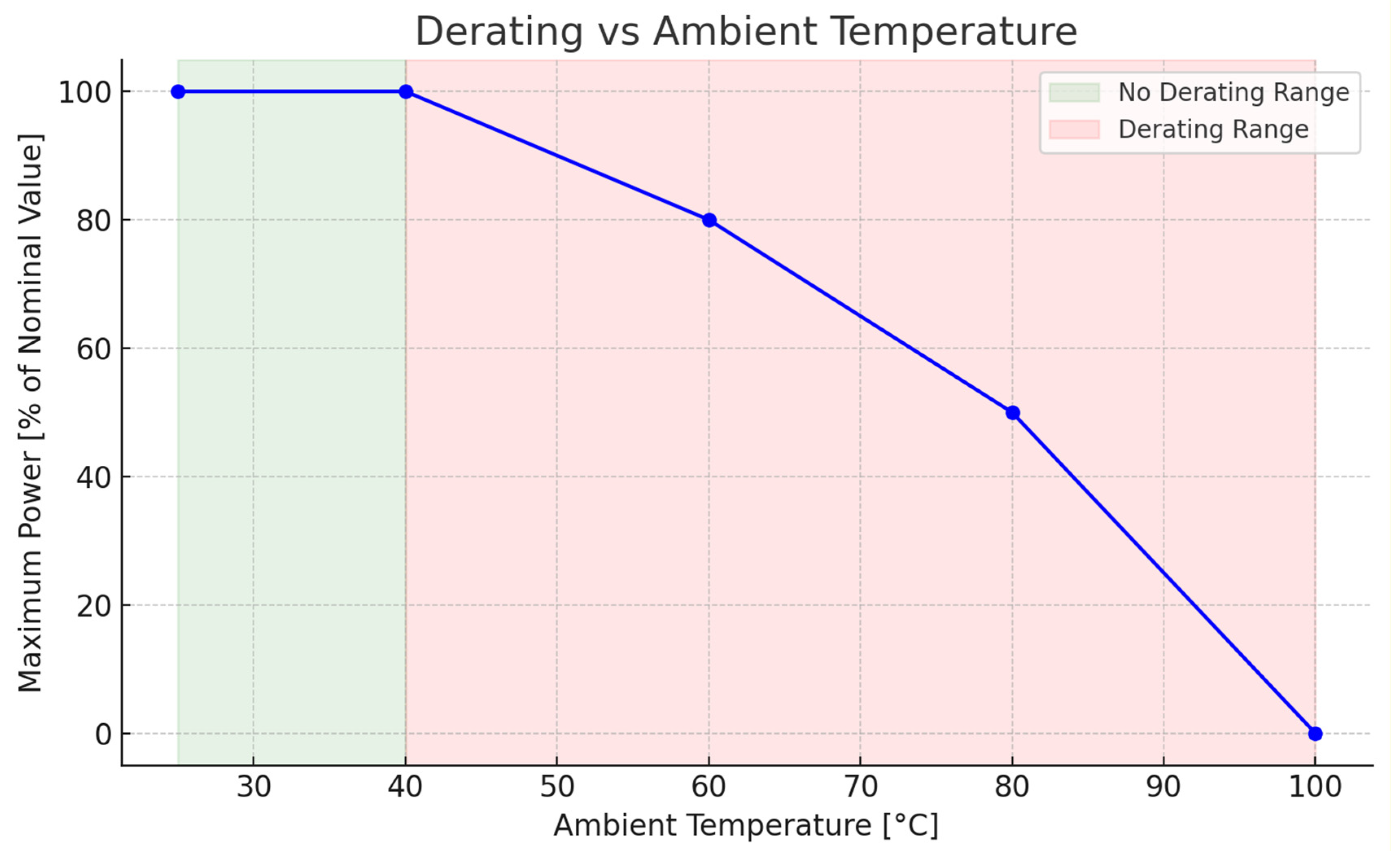
The derating curve illustrates the maximum continuous current that can flow through all possible connections of a component at varying ambient temperatures, up to its specified upper limit [
26].
This upper limit temperature is defined by the materials used in the component. The sum of the ambient temperature and the temperature increase due to current flow (resulting from power loss in resistance) must not exceed this limit; otherwise, the component could be damaged or even completely fail [
26].
As a result, the current-carrying capacity is not a fixed value—it decreases as the surrounding temperature rises. Additionally, factors like the component’s shape, the number of poles, and the type of connected conductors also impact its capacity. To determine this capacity, empirical testing is conducted following the DIN IEC 60512-3 standard [
26].
As illustrated in
Figure 1, the resulting ambient-temperature profile follows the derating behaviour reported by Weidmüller [
27].
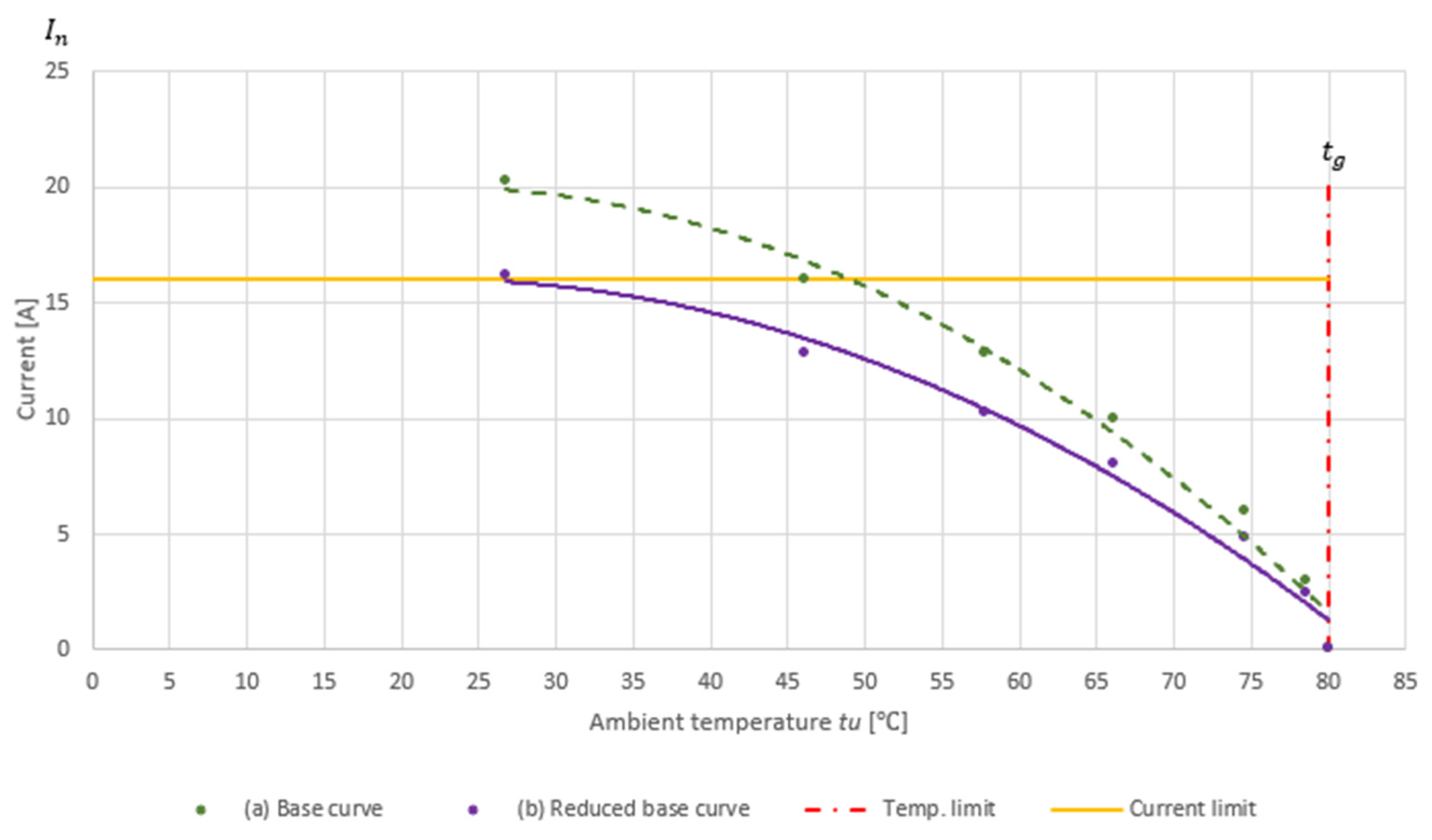
On
Figure 2, the values are represented on the figure using a linear coordinate system to visualize the relationship between current, ambient temperature, and the temperature rise within the component. The
y-axis displays the loading currents, while the
x-axis represents the ambient temperature of the component, where
is the upper limit temperature of component,
is the ambient temperature, and
is the current.
If the derating curve surpasses the current limits in the low ambient temperature range—determined by the current-carrying capacity of the connected conductor cross sections—it should be adjusted to match the lower current value in that range.
2. Materials and Methods
In order to analyze the impact of surface roughness on the derating parameters of electrical contacts, three samples of M12 turned contacts were prepared. The samples were made from the same conductive material CuZn42, following the same geometric and technological specifications, but they differed in the surface roughness of the contact area, expressed as Rz. Two roughness values were selected for the tests:
Rz = 2 μm: representing a high-quality surface that minimizes micronotches and maximizes the actual contact between the components.
Rz = 10 μm: representing a surface of much lower quality, with larger irregularities that reduce the effective contact area.
The selection of R
z = 2 µm and R
z = 10 µm as reference values for surface roughness is based on established industrial and metrological classifications, where lower values indicate smoother, more refined surfaces, and higher values signify increased surface roughness. According to standardized manufacturing and metrology guidelines (e.g., ISO 4287, DIN 4768), surfaces with R
z ≈ 2 µm are typically associated with precision machining, grinding, or polishing, indicative of high-quality surface finishes. In contrast, R
z ≈ 10 µm corresponds to rougher surface textures commonly produced by casting, milling, or rough turning, representing lower-quality finishes. In precision engineering applications, such as those in the aerospace, medical, and high-performance mechanical sectors, an R
z value of 2 µm or lower is desirable, as it contributes to reduced friction, enhanced wear resistance, and improved dimensional accuracy. Conversely, in general manufacturing, surfaces with R
z ≈ 10 µm are often sufficient for non-critical applications, structural components, or parts intended for subsequent finishing processes [
28].
Each sample was prepared using precise turning techniques and checked for compliance with the target Rz parameters using an optical profilometer. The samples were then cleaned to remove any machining residues, such as oils and fine chips, that could interfere with the test results.
The initial contact resistance of each specimen is measured using a low DC current, 16A as recommended for this type of contact cross section, with a four-wire measurement technique. This step ensures accurate resistance readings by minimizing the effects of lead and contact resistance.
The derating test follows the guidelines in DIN EN 60512-5-2 [
29]. Initial setup is based on the electrical contacts being placed in a test circuit with a variable DC power supply. Thermocouples are attached to the contact surfaces to monitor the temperature rise. The contacts are tested under controlled conditions in a temperature- and humidity-regulated chamber.
A stepwise increasing current is applied to the contacts, starting from about 50% of the maximum rated current (Imax). The temperature of the contact surfaces is monitored throughout the test. The current is progressively increased until the temperature stabilizes or reaches the maximum allowable limit.
After determining the maximum current (Imax) that the contact can carry without exceeding the temperature limit, the derating factor of 0.8 (as per DIN EN 60512-5-2) is applied. This means the recommended operational current is 80% of the maximum rated current.
The tests aimed to determine the impact of surface roughness on the maximum allowable operating parameters (e.g., current and temperature) of the M12 contacts. The analysis was to include changes in contact resistance, heat generation, and surface stability under electrical overload conditions. The samples were subjected to:
And the results are summarised in
Table 1.
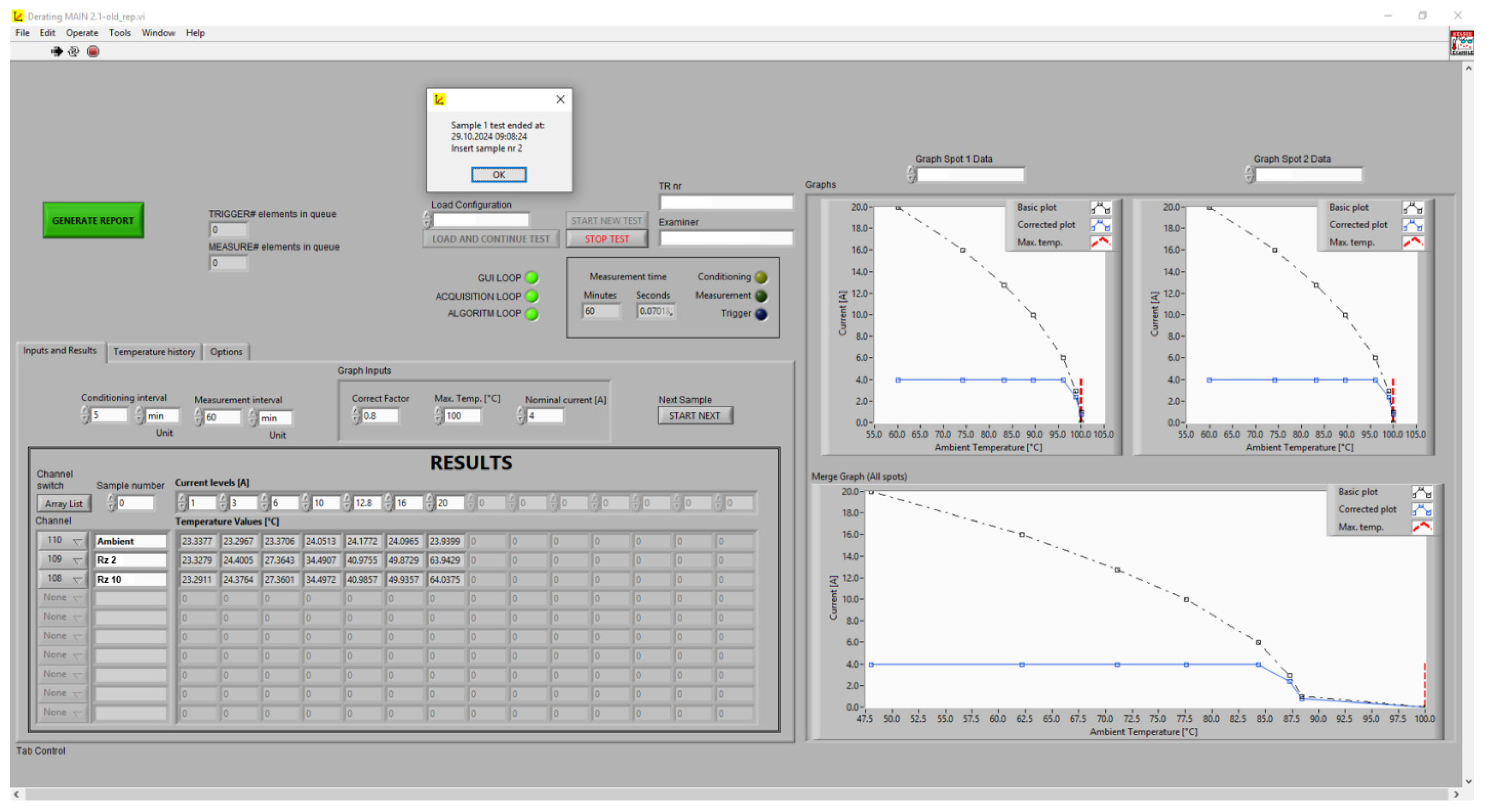
The software interface shown in
Figure 3 is used to conduct derating tests for electrical components, including electrical contacts. The program allows for the analysis of operating parameters such as maximum current, contact resistance, and operating temperatures to determine the limiting conditions of devices based on the environment and load. The program is divided into several functional sections:
INPUTS and RESULTS: A panel for entering test parameters and displaying results.
RESULTS: A table containing test data such as sample number, test current, ambient temperature, and contact resistance values for each sample.
Configuration panel (on the left side):
LOAD CONFIGURATION: The ability to load a previously saved test configuration.
TRIGGER: Indicates the status of the measurement trigger (e.g., activation of the test under specific conditions).
The three graphs visible in the top right corner show the derating test results:
Graph 1 (Current vs. Temp): The relationship between maximum current and ambient temperature.
Graph 2 (Resistance vs. Temp): The relationship between contact resistance and temperature.
Graph 3 (Combined data): A summary of key parameters in one graph.
The graphs display measurement points and trend lines illustrating how parameters change with increasing ambient temperature or current load. The program automatically identifies threshold values, such as the maximum current for a given temperature (intersection point of the graphs), which helps determine derating values.
3. Results
The formula
in DIN EN 60512-5-2 is a standard derating factor used to determine the safe operational current for electrical connectors and conductors. This means that the maximum allowable current should be reduced to 80% of the rated maximum current (Imax) to prevent excessive heating, ensure long-term reliability, and account for real-world variations in operating conditions [
29].
Table 2,
Table 3 and
Table 4 present the measurement data of current values and the corresponding ambient temperatures during testing for R
z2 and R
z10 values. The first row contains the current values in amperes, ranging from 1 A to 20 A. The second row includes the ambient temperature values in degrees Celsius, measured for each current value. The ambient temperature changes depending on the current intensity, but not in a linear manner. The data shows the variation in ambient temperature depending on the measurement conditions.
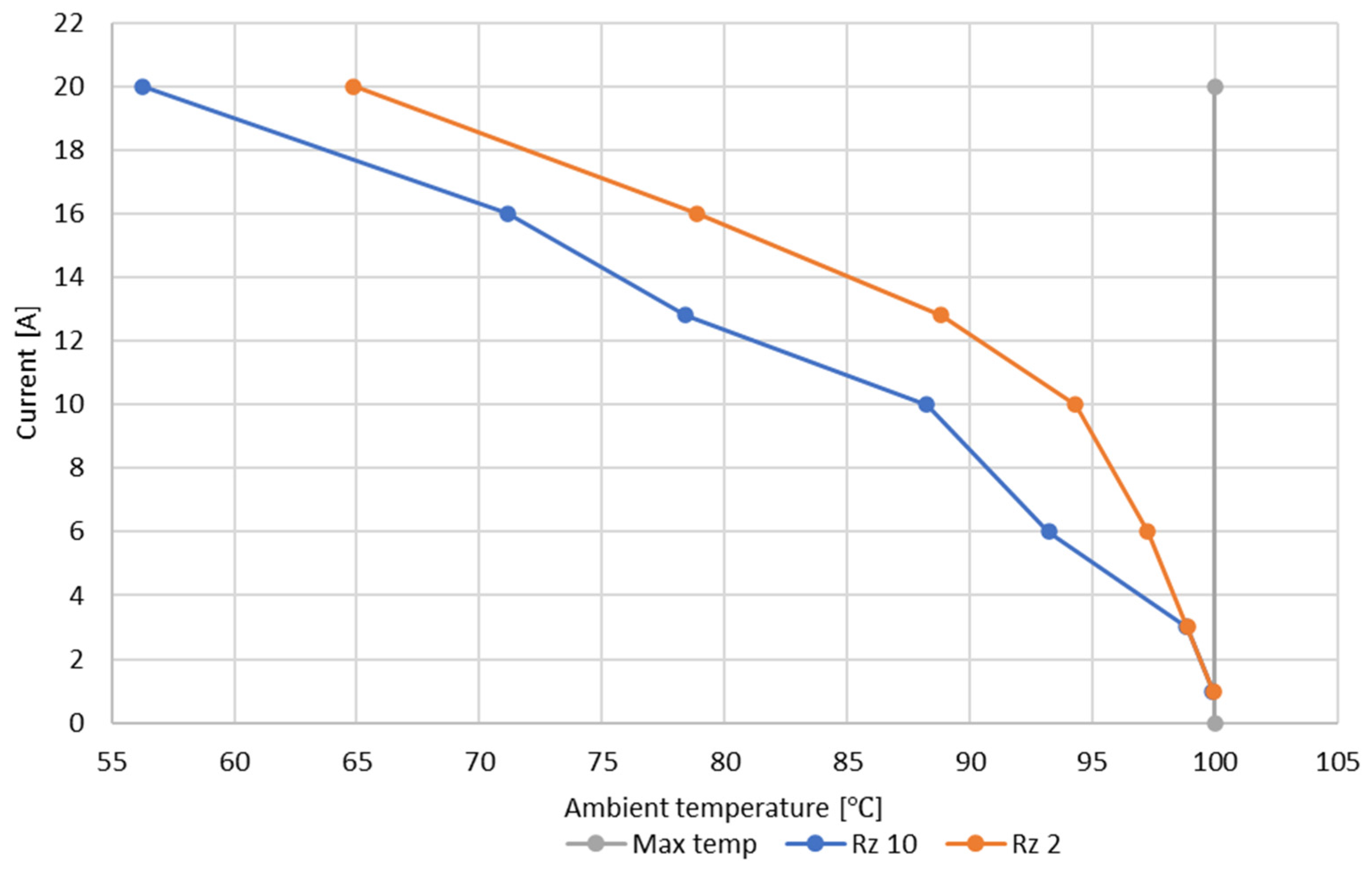
Figure 4 illustrates the relationship between current (A) and ambient temperature (°C) in two different cases, labeled as contact with a roughness of R
z 10 (blue line) and contact with a roughness of R
z 2 (orange line). The horizontal axis represents the ambient temperature ranging from 55 to 100 °C, while the vertical axis shows the current value in amperes, ranging from 0 to 22 A. The current values decrease as the ambient temperature increases, indicating an inverse relationship between these two variables. Additionally, it highlights the maximum temperature (marked by a red dashed line), which is 100 °C. The values for R
z 10 drop slightly faster than for R
z 2, suggesting that at higher R
z values, the current is more sensitive to increases in ambient temperature.
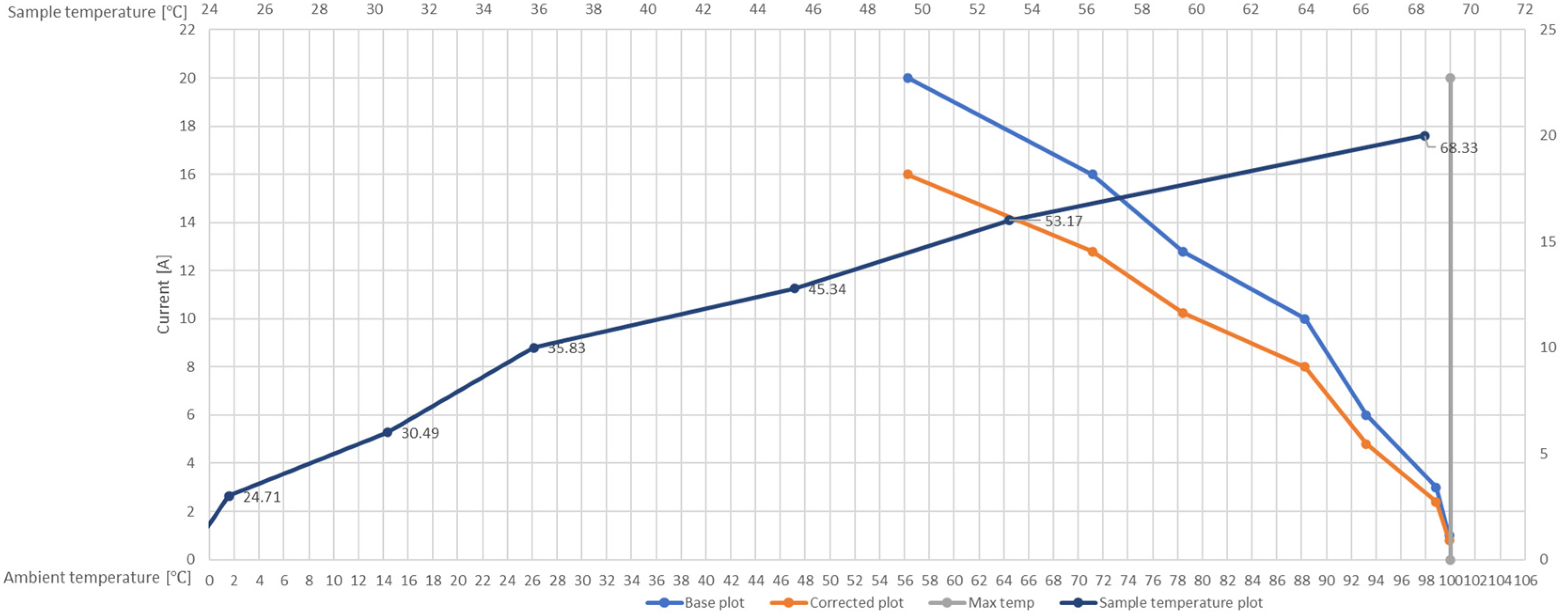
The image (
Figure 5) shows the derating curve for a contact with a surface roughness of R
z10. The graph illustrates the relationship between current (A), ambient temperature (°C), and sample temperature (°C). The vertical axis represents the current value, while the lower horizontal axis denotes the ambient temperature, and the upper horizontal axis indicates the sample temperature. For further context,
Figure 6 complements this plot by charting the allowable current for the same R
z 10 surface as a function of ambient temperature, thereby revealing how thermal constraints tighten as the operating temperature rises.
The curve labeled “Base plot” (orange line) and “Corrected plot” (dashed line) show the gradual decrease in current values with increasing ambient temperature, indicating the limitation of current conduction capability at higher temperatures. The maximum temperature (indicated by the dashed red line) is 100 °C. Additionally, the “Sample temperature plot” (blue line) shows a linear increase in the sample temperature depending on the ambient temperature. The marked points on the figure represent specific current values and their corresponding temperatures. It helps to understand how the increase in temperature affects the ability to conduct current through a contact with a specific roughness.
The table presents values related to the derating curve from the previous graph. It contains data on current, sample temperatures, average temperatures, and temperature increases under various conditions. The first row lists current values in amperes, from 1 A to 20 A, and the second row shows the corrected current values, which gradually increase from 0.8 A to 16 A. The following rows present the temperatures measured for three samples in degrees Celsius, which increase as the current increases, indicating the heating effect.
The “Average” row contains the average temperature values for the three samples in each tested situation. There is a systematic increase in the average temperature from 23.66 °C for the lowest current to 66.66 °C for the highest. The “Temp. increase” row shows the difference between the initial temperature and the final temperature, illustrating the temperature rise from 0.09 °C at 1 A to 42.08 °C at 20 A. The last row, “Max. amb. Temp.”, shows the maximum possible ambient temperature for the given current, decreasing from 99.91 °C at 1 A to 57.92 °C at 20 A. The
Table 5 provides a detailed overview of the impact of current intensity on sample temperatures and the temperature limitations of the contact with roughness R
z10.
The conclusions for contacts with a roughness of Rz10 derived from the presented data highlight the key properties of this type of surface in the context of current conduction and temperature management. The roughness of Rz10 can affect the thermal characteristics of the contact, as seen in the relationship between current and temperature. As the current increases, a systematic rise in the temperature of the samples is observed, which is the result of heat losses due to current conduction through a contact with a specific roughness. The corrected current values indicate a limitation due to temperature, which can be crucial for protecting the material from overheating. The increase in the sample temperature, shown in the table as the difference between the initial and final temperature, grows nonlinearly, meaning that at higher current values, the heating effect is more intense. The maximum allowable ambient temperature decreases with increasing current, reflecting the limitation of operating at higher ambient temperatures under high current loads.
The roughness of Rz10 suggests that the contact may be less effective in terms of heat conduction compared to smoother surfaces. This characteristic may require reducing the maximum current loads to prevent overheating. This could affect the design of systems that require reliable operation under high-load conditions, such as electrical connectors in high-power devices.
In practice, this means that when using materials with this roughness, the thermal effects must be carefully considered in engineering designs. Contacts with a roughness of Rz10 may be suitable for applications with moderate current intensity, but under high-load conditions, additional measures are required to maintain safe operation.
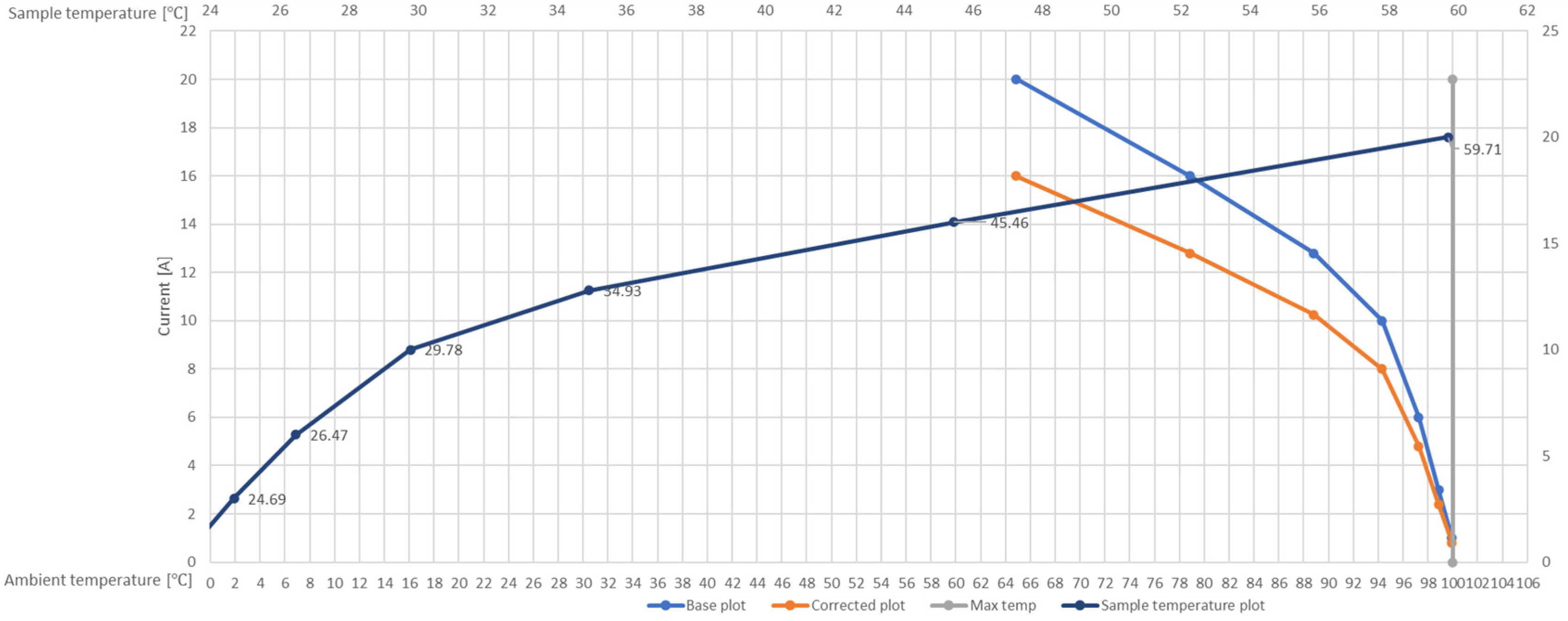
Figure 7 shows the permissible current as a function of ambient temperature, illustrating thermal limitations under increasing load conditions for samples with surface roughness R
z 2. While
Table 6 provides a detailed overview of the impact of current intensity on sample temperatures and the temperature limitations of the contact with roughness R
z 2.
4. Conclusions and Summary
This study provides new scientific insights into the role of surface roughness in shaping the thermal and electrical performance of electrical contacts, particularly in the context of derating behavior. The results demonstrate that surface roughness is not merely a mechanical property but a critical factor influencing contact resistance, thermal conductivity, and overall current-carrying capability.
The analysis of the impact of surface roughness on the derating parameters of electrical contacts revealed significant differences in the behavior of the tested samples. Surfaces with lower roughness (Rz = 2 μm) exhibit higher contact quality, which translates into better current conduction. The larger actual contact area allows for more efficient heat dissipation, reducing the risk of overheating at higher current levels. On the other hand, surfaces with higher roughness (Rz = 10 μm) show greater contact resistance, leading to higher heat losses and a faster temperature rise as the current load increases.
Measurement data indicate a direct correlation between increased contact surface roughness and elevated temperature limitations. Higher current intensities lead to more pronounced thermal loading of the samples, thereby reducing the maximum permissible ambient temperature. The derating characteristics observed for contacts with a surface roughness of Rz = 10 μm demonstrate a heightened sensitivity to ambient temperature variations, as evidenced by a more rapid decline in allowable current with increasing temperature compared to contacts with smoother surfaces.
The thermal tests and contact resistance measurements showed that contacts with smooth surfaces (Rz = 2 μm) are more effective in applications requiring stable operating parameters under high current loads. High roughness (Rz = 10 μm) limits the thermal conductivity of the contacts, requiring the use of lower operating temperatures or reduced maximum current values to avoid overheating. Therefore, when designing systems using electrical contacts, surface roughness parameters must be considered as a key factor influencing their thermal characteristics.
The analysis of the derating characteristics further reveals that the curve corresponding to Rz = 2 μm is notably smoother compared to that of Rz = 10 μm, which exhibits more abrupt temperature increases. The derating behavior for Rz = 2 μm, associated with a smoother contact surface, indicates a more gradual temperature rise with increasing current. In contrast, the Rz = 10 μm curve, representative of a rougher surface, displays pronounced temperature spikes under similar current conditions. This behavior suggests that contacts with lower surface roughness are better suited to sustain higher current loads with reduced thermal stress, whereas those with higher roughness require more stringent thermal management due to their elevated susceptibility to rapid overheating.
The findings of this study underscore the critical role of surface quality in the performance of electrical contacts, particularly in applications demanding high reliability and efficient current conduction. Contacts exhibiting lower surface roughness demonstrate superior suitability for high-load operational conditions, while those with increased roughness are more appropriate for moderate current applications where thermal constraints are less stringent. In practical terms, this necessitates careful thermal analysis and the implementation of effective cooling strategies, especially for contacts with a surface roughness of Rz = 10 μm.
The novel contribution of this work lies in the quantitative assessment of the thermal and electrical implications of contact surface roughness on derating behavior, thereby providing a more rigorous basis for engineering design decisions. Smoother contact surfaces offer enhanced thermal stability and are thus more compatible with high-current, high-reliability environments. Conversely, rougher surfaces exhibit increased susceptibility to thermal stress, limiting their applicability unless accompanied by robust thermal management strategies.
This research advocates for the elevation of surface roughness from a mere manufacturing artifact to a fundamental design parameter. In systems where thermal reliability and energy efficiency are paramount, the surface finish should be integrated into the early stages of design to ensure compliance with contemporary performance standards. The results reaffirm the necessity of stringent surface quality control to meet the evolving demands of modern electrical systems.


