Article

Electronic Structures of Molecular Beam Epitaxially Grown SnSe2 Thin Films on 3×3-Sn Reconstructed Si(111) Surface

by
Zhujuan Li
1,†,
Qichao Tian
1,†,
Kaili Wang
1,
Yuyang Mu
1,
Zhenjie Fan
1,
Xiaodong Qiu
1,
Qinghao Meng
1,
Can Wang
1,2,3 and
Yi Zhang
1,2,4,5,*
1
National Laboratory of Solid State Microstructure, School of Physics, Nanjing University, Nanjing 210093, China
2
Collaborative Innovation Center of Advanced Microstructures, Nanjing University, Nanjing 210093, China
3
Hunan Provincial Key Laboratory of Flexible Electronic Materials Genome Engineering, School of Physics and Electronic Sciences, Changsha University of Science and Technology, Changsha 410114, China
4
Jiangsu Physical Science Research Center, Nanjing University, Nanjing 210093, China
5
Hefei National Laboratory, Hefei 230088, China
*
Author to whom correspondence should be addressed.
These authors contributed equally to this work.
Appl. Sci. 2025, 15(11), 6150; https://doi.org/10.3390/app15116150
Submission received: 7 May 2025 / Revised: 24 May 2025 / Accepted: 28 May 2025 / Published: 29 May 2025

Abstract

:
SnSe2, as a prominent member of the post-transition metal dichalcogenides, exhibits many intriguing physical phenomena and excellent thermoelectric properties, calling for both fundamental study and potential application in two-dimensional (2D) devices. In this article, we realized the molecular beam epitaxial growth of SnSe2 films on a 3 × 3 -Sn reconstructed Si(111) surface. The analysis of reflection high-energy electron diffraction reveals the in-plane lattice orientation as SnSe2[110]// 3 -Sn [112]//Si [110]. In addition, the flat morphology of SnSe2 film was identified by scanning tunneling microscopy (STM), implying the relatively strong adsorption effect of 3 -Sn/Si(111) substrate to the SnSe2 adsorbates. Subsequently, the interfacial charge transfer was observed by X-ray photoemission spectroscopy. Afterwards, the direct characterization of electronic structures was obtained via angle-resolved photoemission spectroscopy. In addition to proving the presence of interfacial charge transfer again, a new relatively flat in-gap band was found in monolayer and few-layer SnSe2, which disappeared in multi-layer SnSe2. The interface strain-induced partial structural phase transition of thin SnSe2 films is presumed to be the reason. Our results provide important information on the characterization and effective modulation of electronic structures of SnSe2 grown on 3 -Sn/Si(111), paving the way for the further study and application of SnSe2 in 2D electronic devices.

1. Introduction

Post-transition metal dichalcogenides (PTMCs), composed of III-VA metal elements (Ga, In, Sn, Bi etc.) and chalcogen elements (S, Se, Te), are a new class of layered two-dimensional (2D) materials that have attracted extensive study recently. In addition to the highly anisotropic lattice structure and unique electronic structures, many outstanding electrochemical, thermoelectric, and optoelectronic properties were observed in PTMCs. Therefore, PTMCs have been applied in many fields like electrochemistry [1,2], electronics [3,4], optoelectronics [5,6] and gas sensing [7]. As a prominent member of PTMCs, SnSe2 is an intrinsic layered semiconductor, exhibiting considerable bandgap and excellent thermoelectric properties like ultra-low thermal conductivity and high carrier mobility [8,9]. Together with a high abundance of Sn, SnSe2 shows potential applications in optoelectronics [10,11,12,13], thermoelectric devices [14], lithium-ion batteries [15] and phase change memory [16,17].
In addition, intriguing physical properties like charge density wave (CDW), superconductivity and interfacial polarons were observed in SnSe2 from previous works [18,19,20]. The interface properties of monolayer (ML) SnSe2 could be effectively tuned by choosing different substrates. For examples, a recent study showed that ML and bilayer SnSe2 films grown on Si(111) undergo a commensurate CDW transition at TC ~78 K driven by Fermi surface nesting between symmetry inequivalent electron pockets, forming a corresponding (2 × 2) superlattice [20]. In addition, the formation of interfacial polarons induced by charge accumulation and electron–phonon coupling between SrTiO3 and SnSe2 was evidenced [19]. Furthermore, the superconductivity in SnSe2, which can be modulated by cation intercalation [21] and dielectric gating techniques [22], was reported to be enhanced in the epitaxial SnSe2 on graphitized SiC(0001) substrate [18]. However, there are only a few studies on SnSe2 film grown on Si(111), with the study on direct characterization of band structures still lacking in particular. In this paper, we synthesize SnSe2 films on Si(111) by molecular beam epitaxy (MBE), and employ in situ reflection high energy electron diffraction (RHEED), scanning tunneling microscopy (STM), X-ray photoemission spectroscopy (XPS) and angle-resolved photoemission spectroscopy (ARPES) to characterize the atomic and electronic structures of them. We found that the SnSe2 shows layer-by-layer growth mode on 3 -Sn/Si(111) substrate with a high quality of flatness. The interfacial charge transfer effect is observed in the SnSe2 film grown on 3 -Sn/Si(111) substrate. Moreover, an emerging band above the original valence band of bulk SnSe2 is found in the SnSe2 thin film, resulting in the reduction of the indirect band gap. This emerging band is suggested to be induced by the interfacial strain-driven structural phase transition of the grown SnSe2. Our results provide important information for further applications of SnSe2 film in 2D electronic devices.

2. Materials and Methods

All of the experiments were performed in a combined MBE-STM-ARPES ultra-high vacuum (UHV) system with a base pressure of ~2 × 10⁻¹⁰ mbar. First, to obtain a clean Si(111)-(7 × 7) reconstructed surface, a Si(111) substrate (n-doped by P) was initially degassed at 650   ° C , followed by flash-annealing to ~ 1250   ° C for 20 cycles. To passivate the dangling bonds of the Si(111)-(7 × 7) surface and enhance the surface diffusion for the growth of SnSe2, we evaporated 1 / 3 ML of Sn on the Si(111)-(7 × 7) surface at 550   ° C , leading to a well-ordered 3 × 3   R 30 ° -Sn recontruction surface on the Si(111) ( 3 -Sn/Si(111)) surface. Next, the SnSe2 films were grown by co-depositing high-purity Sn (99.99%) and Se (99.99%) from standard Knudsen cells separately onto the 3 -Sn/Si(111) substrate at 200   ° C . The temperatures of the Sn and Se sources were maintained at 920   ° C and 130   ° C , respectively, keeping the flux ratio at Sn:Se ~1:20, and leading the growth rate of SnSe2 films as about ~15 min/layer. During the film growth, an in situ RHEED was used for real time monitoring and surface structural characterization. The electron beam energy of RHEED was kept at 18 keV. After growth, the surface morphology was further characterized by an in situ room temperature STM (RT-STM), whose set point was kept at Vb = 1.0 V and It = 100 pA. Subsequently, to investigate the electronic structures, the in situ low temperature (~10 K) XPS and ARPES were performed by a shared DA30 analyzer (Scienta Omicron AB, Uppsala, Sweden). The monochromatic X-ray of XPS and the ultraviolet light source of ARPES were generated from an Al electrode excitation source (Al Kα, 1486.7 eV) and a Helium lamp with a monochromator (He I, 21.218 eV), respectively.

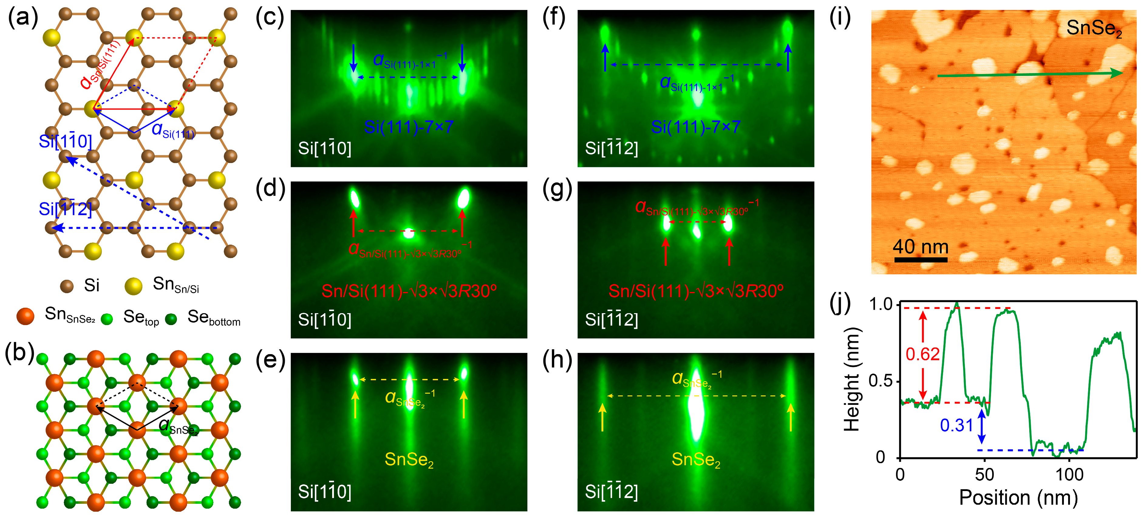
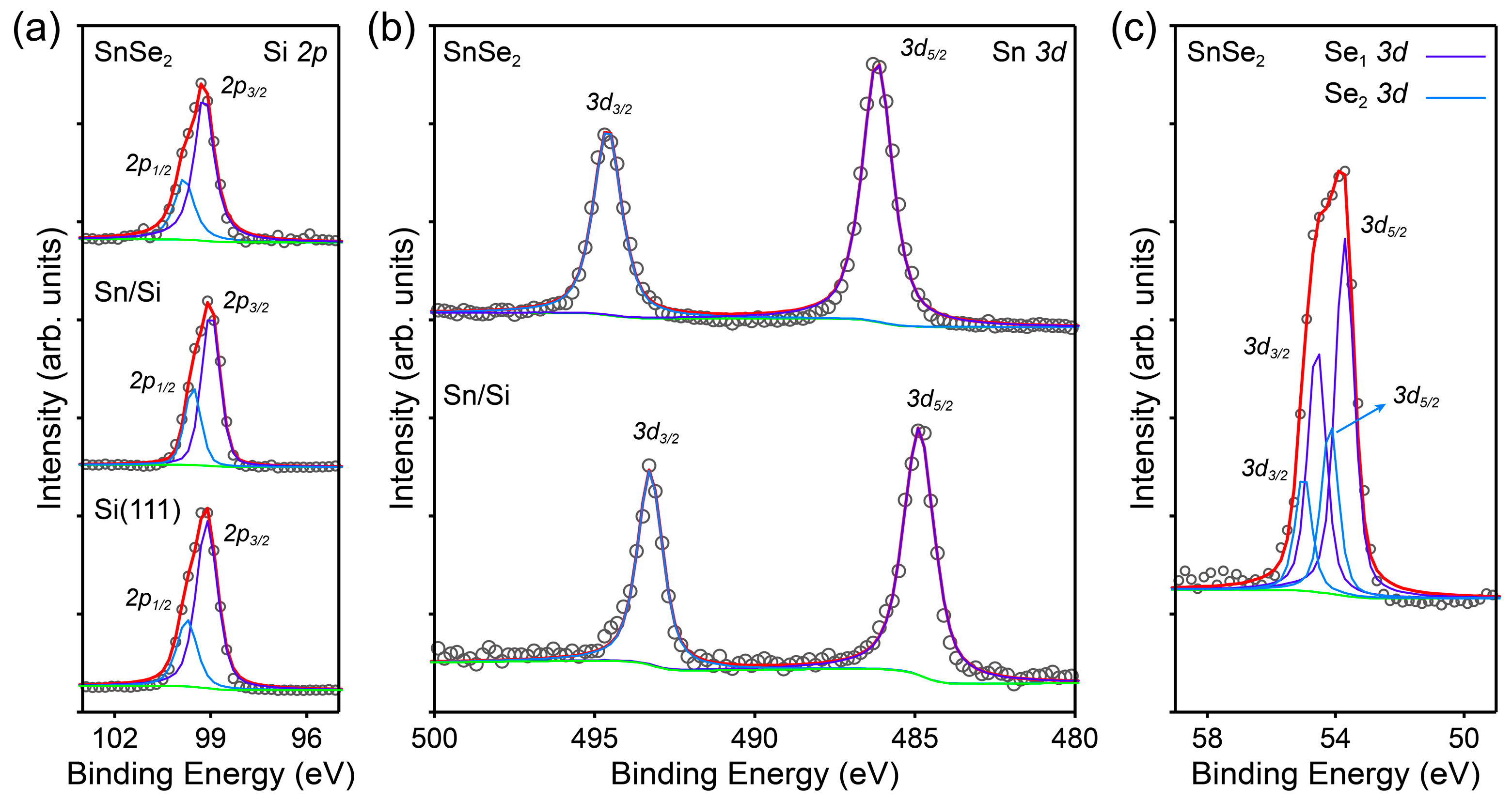
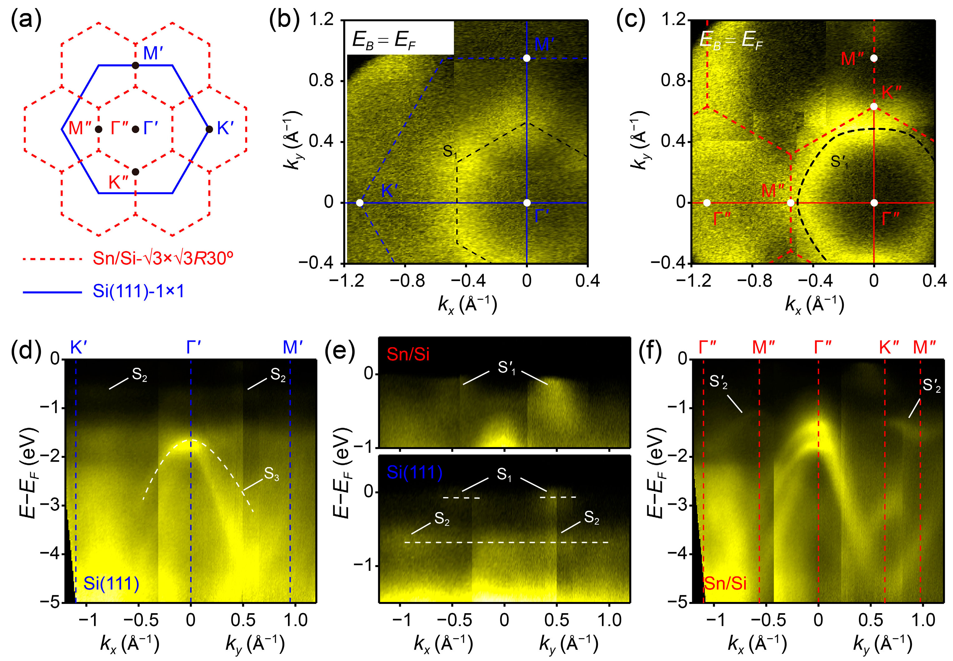
3. Results and Discussion

The lattice structure of the 3 -Sn/Si(111) surface is illustrated in Figure 1a, showing an in-plane 30° rotation and 3 × 3 reconstruction of a Sn layer relative to a Si(111) surface. Each Sn atom is back-bonded to three Si atoms beneath, with a remaining dangling bond at the surface. Figure 1b presents the lattice structure of T-phase SnSe2 (T-SnSe2). As a typical MX2 of PTMCs, single layer T-SnSe2 consists of two layers of chalcogenides and a layer of transition metal sandwiched between them, presenting a Se-Sn-Se sandwich-like structure. Within the layer, covalent bonding is achieved through Se-Sn, while interlayer stacking is achieved through Se-Se van der Waals interactions, presenting the lattice constants as a = 3.81   Å and c = 6.14   Å [23].
Figure 1c–e present the RHEED patterns of an annealed Si(111)-(7 × 7) surface, a 3 -Sn/Si(111) surface and an ML SnSe2 film along the Si 1 1 ¯ 0 direction, respectively. Corresponding RHEED patterns along the Si 1 ¯ 1 ¯ 2 direction are also obtained by 30° rotating the sample in-plane, as shown in Figure 1f–h. From Figure 1c,f, we can see the clearly (7 × 7) reconstructed patterns of the annealed Si surface, which disappear and are displaced by a new pair of (1 × 1) diffraction stripes after the 3 -Sn passivation, as shown in Figure 1d,g. Subsequently, from Figure 1e,h, we can see the new (1 × 1) diffraction stripes from the epitaxial SnSe2 film, which are very clear and sharp, implying the high-quality crystallization.
By performing Lorentz fittings on the corresponding RHEED patterns, we can accurately obtain the (1 × 1) main diffraction stripe spacings of both substrates and the SnSe2 films (see Figure S1 of the Supplementary Materials for details), on which we can conduct more detailed analysis and calculations. The orientation of the 3 -Sn buffer layer is in-plane rotated by 30° relative to the Si(111), with the calculated lattice constant as a 3 Sn = 6.66 ± 0.05   , approximately equal to 3 times a Si 111 = 3.84   . This result is consistent with the previous reports [24,25]. Subsequently, the epitaxial SnSe2 film is rotated by 30° again relative to the 3 -Sn/Si surface, resulting in the same in-plane orientation with the Si(111) substrate. Furthermore, the in-plane lattice constant of ML SnSe2 is also obtained as a SnSe 2 = 3.83 ± 0.05   , which is in agreement with the previous report [23], and shows no obvious interfacial strain effect considering the ± 0.05   errors in RHEED analysis.
After growth, we utilized the in situ STM to investigate the surface morphology of ML SnSe2 grown on 3 -Sn/Si(111), as shown in Figure 1i. Different from three-dimensional (3D) island growth mode on graphene substrates [26], the SnSe2 grown on 3 -Sn/Si(111) tends to be layer-by-layer growth mode, which provides the better film flatness. The different growth modes of SnSe2 on two substrates may be attributed to the larger local density of states of 3 -Sn/Si(111) than that of graphene substrate, leading to an increased interface adsorption ability [27,28]. The height of ML SnSe2 is ~0.62 Å [Figure 1j], which is consistent with the previous report [23].
Having determined the lattice structure, we then investigated the chemical states of the SnSe2 film via in situ XPS. The full XPS spectra of Si(111), 3 -Sn/Si(111) and SnSe2 are shown in the Supplementary Materials Figure S2. Figure 2a presents the Si 2p core-level spectra of the Si(111)-(7 × 7) surface, 3 -Sn/Si(111) and ML SnSe2 film. For the Si(111)-(7 × 7) surface, the core levels of Si 2p1/2 and Si 2p3/2 orbitals are located at 99.7 eV and 99.1 eV, in accordance with the previous literature [29]. The peaks red-shift by about 0.1 eV compared to the core levels of Si 2p1/2 (99.6 eV) and Si 2p3/2 (99.0 eV) orbitals of the 3 -Sn/Si(111), indicating a charge transfer effect from Sn to Si upon the surface Sn-Si bond formation, which is reasonable since the electronegativity of Si is stronger than that of Sn. In addition, after the growth of ML SnSe2, the core levels of Si 2p1/2 (99.8 eV) and Si 2p3/2 (99.2 eV) again shift toward higher binding energies, which suggests interfacial charge transfer from the 3 -Sn/Si(111) substrate to ML SnSe2.
Subsequently, in Figure 2b, the core levels of Sn 3d3/2 (493.3 eV) and 3d5/2 (484.9 eV) orbitals of 3 -Sn/Si(111) exhibit obvious blue-shift compared to the core levels of Sn 3d3/2 (494.6 eV) and 3d5/2 (486.2 eV) orbitals of ML SnSe2. This shift can be explained by the much stronger bond polarity of Sn-Se than that of Sn-Si, which leads to the weakened screening to the Coulomb potential created by the positive core of Sn, and finally resulting in the higher binding energies of the remaining electrons. Moreover, in Figure 2c the core levels of Se 3d orbitals of ML SnSe2 split into two sets, Se1 3d3/2 (54.6 eV) and Se1 3d5/2 (53.7 eV), and Se2 3d3/2 (55.0 eV) and Se2 3d5/2 (54.2 eV), respectively. The splitting of Se 3d orbitals implies the presence of two nonequivalent chemical environments of Se atoms in ML SnSe2. This can be attributed to the fact that the bottom layer of Se atoms is adjacent to the √3-Sn surface, while the top layer of Se atoms is located at the top surface of SnSe2.
To further investigate the interface effect, we characterized the electronic structures of the SnSe2/ 3 -Sn/Si(111) system via in situ ARPES. Figure 3 shows the electronic structures of the Si(111)-(7 × 7) and 3 -Sn/Si(111) surface. The constant energy mappings near the Fermi level of the Si(111)-(7 × 7) and 3 -Sn/Si(111) surface clearly display the six-fold symmetry and the relative 30° rotation with respect to each other [Figure 3b,c], in accordance with the corresponding schematic of the Brillouin zone (BZ) illustrated in Figure 3a. The band structure of Si(111)-(7 × 7) surface is shown in Figure 3d, with the intensity enhanced zoom-in spectra plotted at the bottom panel of Figure 3e for more detailed observation. Three surface states marked as S1, S2 and S3 can be clearly observed, in agreement with the previous literature [30]. The S3 is induced by the back bonds of the (7 × 7) reconstruction, showing the obvious band dispersion with its maximum located at about −1.8 eV. The nearly flat S2, induced by the rest-atoms, is located at about −0.9 eV, while the S1, induced by the adatoms of the surface reconstruction, lies near the Fermi level.
The band structure of the 3 -Sn/Si(111) surface and its zoom-in spectra with enhanced intensity are plotted in Figure 3f and the top panel of Figure 3e, respectively. The surface states S2’ is located at −1~−2 eV, and the minimum of surface states S1’ is located at −0.7 eV. The S2’ and S1’ are attributed to the three back bonds with Si and the one remaining dangling bond of each Sn adatom, respectively [31,32]. Our results indicate the well processed substrate, on which the SnSe2 films can be grown with high-quality flatness and crystallization.
Finally, we investigated the electronic structures of SnSe2 films grown on the 3 -Sn/Si(111) surface, as shown in Figure 4. Recent first-principles calculations and an ARPES study of SnSe2 showed that bulk SnSe2 possesses an indirect band gap of ~1.07 eV, whose conduction band minimum (CBM) and valence band maximum (VBM) are located along the M-L and Γ-M (K) directions, respectively [33,34]. In contrast, ML SnSe2 film exhibits an indirect band gap of ~1.69 eV, with CBM and VBM located at the M and Γ points, respectively [34]. The increased band gap of ML SnSe2 is attributed to the quantum confinement of electrons in quasi-2D samples and the reduction of the screening. The CBM of both ML and bulk SnSe2 are higher than the Fermi level, making it difficult to be characterized directly via ARPES in pristine SnSe2.
Figure 4a is the constant energy mapping taken near the Fermi level of ML SnSe2, presenting clear six-fold symmetry, with electron pockets centered at the M points of BZ. It is quite similar to that of the potassium(K)-doped SnSe2 single crystals, suggesting the charge transfer from the 3 -Sn/Si(111) substrate to the grown SnSe2 film. In addition, the CBM of different layers of SnSe2 are obtained from energy distribution curve (EDC) fittings, as shown in Figure S3. It can be clearly seen that all the CBM features appear near the Fermi level at the M point, shifting from −199 meV in ML SnSe2 to −112 meV in few-layer (FL) SnSe2 (the thickness of FL SnSe2 is estimated to be ~3 ML), and finally to the edge of the Fermi level in multi-layer (Multi-L, the estimated thickness is about ~6 ML) SnSe2 [Figure 4i–k]. The upward shift in CBM with the increase in layers again confirms the interfacial charge transfer scenario.
Furthermore, the ARPES spectra of ML, FL and Mult-L SnSe2 along the Γ-M direction are plotted in Figure 4b–d, respectively. The VBM are all located at the Γ point. For more detailed observation, the zoom-in ARPES spectra near the VBM around the Γ point and corresponding EDCs along the red lines are illustrated in Figure 4e–h. Intriguingly, we note that a new band α above the original VBM of bulk SnSe2 emerges in the ML and FL SnSe2 films, which disappears in the Mult-L SnSe2. The emerging α band can be better resolved in the second-derivative spectra, as shown in Figure S4. From the EDC fittings in Figure 4h, the maximum of the α band is located at −1.05 eV and −0.97 eV in ML and FL SnSe2, respectively, leading to the reduced band gaps as 0.85 eV in both of them. The position, as well as the relatively flat dispersion of the α band, is quite similar to the top valence band of H-phase SnSe2 (H-SnSe2), which was characterized and marked as ‘7/8’ band in a previous study [35]. Moreover, a recent first-principle calculation showed a reduced band gap of H-SnSe2 compared to T-SnSe2, in accordance with our ARPES results [36]. Therefore, we believe that the newly emerged energy band α would be attributed to the presence of a small amount of H-SnSe2 formed in ML and FL SnSe2. Indeed, a pressure-induced structural phase transition to H-SnSe2 has been reported before [37]. Therefore, we assume that the interfacial strain from 3 -Sn/Si(111) substrate would be the main reason for the emergence of H-SnSe2, which vanishes gradually as the film becomes thicker. Similar interfacial-induced structural phase transitions in other 2D materials were also observed in previous studies. For example, the lattice structure of WSe2 grown on SrTiO3 substrate was 1T’-phase [38], while the mixture of 1T’- and 1H-phase WSe2 was found on graphene [39,40]. However, this interfacial strain effect is hard to be directly detected by RHEED due to the large relative error (~1.3%) in RHEED analysis, while the lattice constants of H-SnSe2 and T-SnSe2 are quite similar. Furthermore, the indistinct band structures of ML and FL SnSe2, contrary to the clear band structures in Multi-L SnSe2, also provide evidence for our assumption, since the band structures of both T-SnSe2 and H-SnSe2 can be detected by ARPES and eventually overlap together in the spectra, as shown in Figure 4b,c.
Our results indicate the potential application prospects of SnSe2/ 3 -Sn/Si(111) in 2D devices. First of all, the Si is a traditional semiconductor with mature large-scale device fabrication processes, which is beneficial for the practical application of SnSe2 grown on Si substrate. Actually, there have been several studies on SnSe2/Si-based 3D devices in the past, such as temperature-dependent phase change memory [17] and self-powered broadband photodetectors which can be enhanced by Rhenium doping [12,13]. In our study, the 3 -Sn passivated Si(111) substrate can not only effectively prevent the formation of Sn and Se clusters on the surface of Si, but also provide relatively strong adsorption effects, which allows us to achieve the growth of SnSe2/ 3 -Sn/Si(111) thin films with better crystallization and film flatness. Moreover, the interfacial charge transfer gives rise to the n-doped SnSe2 film, allowing us to build atomically thin SnSe2-based p-n junction devices. Furthermore, our results also show that the band gap of thin SnSe2 film grown on 3 -Sn/Si(111) substrate can be more effectively modulated by changing the number of layers because of the appearing α band in ML and FL SnSe2. Therefore, SnSe2/ 3 -Sn/Si(111) would appeal to higher performance tunable, broad-spectrum photodetection, showing its possible application in 2D optoelectronics. In addition, the possible partial lattice distortion may lead to changes in resistivity, indicating its prospect in phase change memory application. However, to determine the specific performance of the SnSe2/ 3 -Sn/Si(111) system, electric transport measurements are still needed to further explore its application prospects.

4. Conclusions

In summary, we have realized the MBE growth of SnSe2 films on 3 -Sn passivated Si(111) substrate. The analysis of RHEED patterns demonstrates the successful growth and the same in-plane lattice orientation of the grown SnSe2 with Si(111) substrate, whereas the Sn buffer layer conducts a 3 × 3 reconstruction with in-plane rotation by 30° relative to both Si(111) and SnSe2. In addition, the layer-by-layer growth mode of SnSe2 identified by STM indicates the relatively stronger adsorption effect of 3 -Sn/Si(111) on SnSe2 adsorbates than the commonly used graphene substrate. Subsequently, from the XPS measurements, we observed the interfacial charge transfer from substrate to SnSe2, which was further confirmed in the ARPES measurements. Moreover, a new valence band α located above the original VBM of bulk SnSe2 emerges in the ML and FL SnSe2 films, which disappears in the Multi-L SnSe2 film. We attribute it to the partial T→H structural phase transition of thin SnSe2 films grown on 3 -Sn/Si(111) substrate, probably driven by the interfacial strain. The direct characterizations of electronic structures of SnSe2 films, as well as the layer-dependent structural transition, along with the effective band modulation provide significant and important information for the further applications of SnSe2 films in 2D electronic devices, such as optoelectronics and phase change memory.

Supplementary Materials

The following supporting information can be downloaded at: https://www.mdpi.com/article/10.3390/app15116150/s1, Section SA. Method for calculating lattice constants from RHEED patterns; Section SB. Full XPS spectra; Section SC. EDCs fitting for determining the CBMs; Section SD. Second-derivative ARPES spectra.

Author Contributions

Conceptualization, Y.Z.; methodology, Z.L., Q.T., K.W., Y.M., Z.F., X.Q., Q.M., C.W. and Y.Z.; software, Y.Z.; validation, Z.L., Q.T., K.W., Y.M. and Y.Z.; formal analysis, Z.L., Q.T., K.W., Y.M. and Y.Z.; investigation, Z.L. and Q.T.; resources, Y.Z.; data curation, Z.L., Q.T., K.W., Y.M. and Y.Z.; writing—original draft preparation, Z.L.; writing—review and editing, Y.Z.; visualization, Z.L., Q.T., K.W. and Y.M.; supervision, C.W. and Y.Z.; project administration, Y.Z.; funding acquisition, Y.Z. All authors have read and agreed to the published version of the manuscript.

Funding

This research was funded by the National Natural Science Foundation of China (No. 92165205), the Fundamental Research Funds for the Central University (No. 0204/14380228), the Fundamental Research Program of Natural Science Foundation of Jiangsu Province (BK20243011), and the Natural Science Foundation of Hunan Province of China (No. 2024jj6009).

Institutional Review Board Statement

Not applicable.

Informed Consent Statement

Not applicable.

Data Availability Statement

The raw data supporting the conclusions of this article will be made available by the authors on request.

Conflicts of Interest

The authors declare no conflicts of interest.

Abbreviations

The following abbreviations are used in this manuscript:
2DTwo-dimensional
PTMCsPost-transition metal dichalcogenides
CDWCharge density wave
MLMonolayer
MBEMolecular beam epitaxy
RHEEDReflection high energy electron diffraction
STMScanning tunneling microscopy
XPSX-ray photoemission spectroscopy
ARPESAngle-resolved photoemission spectroscopy
UHVUltra-high-vacuum
3DThree-dimensional
BZBrillouin zone
CBMConduction band minimum
VBMValence band maximum
EDCEnergy distribution curve
FLFew-layer
Multi-LMulti-layer

References

  1. Tan, S.M.; Chua, C.K.; Sedmidubský, D.; Sofer, Z.B.; Pumera, M. Electrochemistry of layered GaSe and GeS: Applications to ORR, OER and HER. Phys. Chem. Chem. Phys. 2016, 18, 1699–1711. [Google Scholar] [CrossRef]
  2. Wang, Y.; Szökölová, K.; Nasir, M.Z.M.; Sofer, Z.; Pumera, M. Electrochemistry of Layered Semiconducting AIIIBVI Chalcogenides: Indium Monochalcogenides (InS, InSe, InTe). ChemCatChem 2019, 11, 2634–2642. [Google Scholar] [CrossRef]
  3. Sucharitakul, S.; Goble, N.J.; Kumar, U.R.; Sankar, R.; Bogorad, Z.A.; Chou, F.-C.; Chen, Y.-T.; Gao, X.P.A. Intrinsic Electron Mobility Exceeding 103 cm2/(V s) in Multilayer InSe FETs. Nano Lett. 2015, 15, 3815–3819. [Google Scholar] [CrossRef] [PubMed]
  4. Xu, K.; Yin, L.; Huang, Y.; Shifa, T.A.; Chu, J.; Wang, F.; Cheng, R.; Wang, Z.; He, J. Synthesis, properties and applications of 2D layered MIIIXVI (M = Ga, In; X = S, Se, Te) materials. Nanoscale 2016, 8, 16802–16818. [Google Scholar] [CrossRef]
  5. Hu, P.; Wen, Z.; Wang, L.; Tan, P.; Xiao, K. Synthesis of few-layer GaSe nanosheets for high performance photodetectors. ACS Nano 2012, 6, 5988–5994. [Google Scholar] [CrossRef]
  6. Hu, P.; Zhang, J.; Yoon, M.; Qiao, X.-F.; Zhang, X.; Feng, W.; Tan, P.; Zheng, W.; Liu, J.; Wang, X.; et al. Highly sensitive phototransistors based on two-dimensional GaTe nanosheets with direct bandgap. Nano Res. 2014, 7, 694–703. [Google Scholar] [CrossRef]
  7. Marvan, P.; Mazánek, V.; Sofer, Z. Shear-force exfoliation of indium and gallium chalcogenides for selective gas sensing applications. Nanoscale 2019, 11, 4310–4317. [Google Scholar] [CrossRef]
  8. Li, G.; Ding, G.; Gao, G. Thermoelectric properties of SnSe2 monolayer. J. Phys. Condens. Matter 2017, 29, 015001. [Google Scholar] [CrossRef] [PubMed]
  9. Shafique, A.; Samad, A.; Shin, Y.-H. Ultra low lattice thermal conductivity and high carrier mobility of monolayer SnS2 and SnSe2: A first principles study. Phys. Chem. Chem. Phys. 2017, 19, 20677–20683. [Google Scholar] [CrossRef]
  10. Huang, Y.; Xu, K.; Wang, Z.; Shifa, T.A.; Wang, Q.; Wang, F.; Jiang, C.; He, J. Designing the shape evolution of SnSe2 nanosheets and their optoelectronic properties. Nanoscale 2015, 7, 17375–17380. [Google Scholar] [CrossRef]
  11. Zhou, X.; Gan, L.; Tian, W.; Zhang, Q.; Jin, S.; Li, H.; Bando, Y.; Golberg, D.; Zhai, T. Ultrathin SnSe2 Flakes Grown by Chemical Vapor Deposition for High-Performance Photodetectors. Adv. Mater. 2015, 27, 8035–8041. [Google Scholar] [CrossRef] [PubMed]
  12. Kumar, M.; Huang, B.-R.; Saravanan, A.; Sun, H.; Chen, S.-C. Self-Powered Broadband Photodetectors Based on Si/SnS2 and Si/SnSe2 p–n Heterostructures. Adv. Electron. Mater. 2024, 10, 2400164. [Google Scholar] [CrossRef]
  13. Chauhan, P.; Patel, A.B.; Solanki, G.K.; Patel, K.D.; Pathak, V.M.; Sumesh, C.K.; Narayan, S.; Jha, P.K. Rhenium substitutional doping for enhanced photoresponse of n-SnSe2/p-Si heterojunction based tunable and high-performance visible-light photodetector. Appl. Surf. Sci. 2021, 536, 147739. [Google Scholar] [CrossRef]
  14. Luo, Y.; Zheng, Y.; Luo, Z.; Hao, S.; Du, C.; Liang, Q.; Li, Z.; Khor, K.A.; Hippalgaonkar, K.; Xu, J.; et al. n-Type SnSe2 Oriented-Nanoplate-Based Pellets for High Thermoelectric Performance. Adv. Energy Mater. 2018, 8, 1702167. [Google Scholar] [CrossRef]
  15. Choi, J.; Jin, J.; Jung, I.G.; Kim, J.M.; Kim, H.J.; Son, S.U. SnSe2 nanoplate–graphene composites as anode materials for lithium ion batteries. Chem. Commun. 2011, 47, 5241–5243. [Google Scholar] [CrossRef]
  16. Wang, R.Y.; Caldwell, M.A.; Jeyasingh, R.G.D.; Aloni, S.; Shelby, R.M.; Wong, H.S.P.; Milliron, D.J. Electronic and optical switching of solution-phase deposited SnSe2 phase change memory material. J. Appl. Phys. 2011, 109, 113506. [Google Scholar] [CrossRef]
  17. Sun, M.; Yifeng, H.; Bo, S.; Jiwei, Z.; Sannian, S.; Song, Z. Si/SnSe2 Multilayer Films for Phase Change Memory Applications. Integr. Ferroelectr. 2012, 140, 1–7. [Google Scholar] [CrossRef]
  18. Zhang, Y.-M.; Fan, J.-Q.; Wang, W.-L.; Zhang, D.; Wang, L.; Li, W.; He, K.; Song, C.-L.; Ma, X.-C.; Xue, Q.-K. Observation of interface superconductivity in a SnSe2 epitaxial graphene van der Waals heterostructure. Phys. Rev. B 2018, 98, 220508. [Google Scholar] [CrossRef]
  19. Mao, Y.; Ma, X.; Wu, D.; Lin, C.; Shan, H.; Wu, X.; Zhao, J.; Zhao, A.; Wang, B. Interfacial Polarons in van der Waals Heterojunction of Monolayer SnSe2 on SrTiO3 (001). Nano Lett. 2020, 20, 8067. [Google Scholar] [CrossRef]
  20. Wang, S.-Z.; Zhang, Y.-M.; Fan, J.-Q.; Ren, M.-Q.; Song, C.-L.; Ma, X.-C.; Xue, Q.-K. Charge density waves and Fermi level pinning in monolayer and bilayer SnSe2. Phys. Rev. B 2020, 102, 241408. [Google Scholar] [CrossRef]
  21. Wu, H.; Li, S.; Susner, M.; Kwon, S.; Kim, M.; Haugan, T.; Lv, B. Spacing dependent and cation doping independent superconductivity in intercalated 1T 2D SnSe2. 2D Mater. 2019, 6, 045048. [Google Scholar] [CrossRef]
  22. Zeng, J.; Liu, E.; Fu, Y.; Chen, Z.; Pan, C.; Wang, C.; Wang, M.; Wang, Y.; Xu, K.; Cai, S.; et al. Gate-Induced Interfacial Superconductivity in 1T-SnSe2. Nano Lett. 2018, 18, 1410–1415. [Google Scholar] [CrossRef] [PubMed]
  23. Schlüter, M.; Cohen, M.L. Valence-band density of states and chemical bonding for several non-transition-metal layer compounds: SnSe2, PbI2, BiI3, and GaSe. Phys. Rev. B 1976, 14, 424. [Google Scholar] [CrossRef]
  24. Zhachuk, R.A.; Rogilo, D.I.; Petrov, A.S.; Sheglov, D.V.; Latyshev, A.V.; Colonna, S.; Ronci, F. Atomic structure of a single step and dynamics of Sn adatoms on the Si(111)−√3×√3-Sn surface. Phys. Rev. B 2021, 104, 125437. [Google Scholar] [CrossRef]
  25. Wu, X.; Ming, F.; Smith, T.S.; Liu, G.; Ye, F.; Wang, K.; Johnston, S.; Weitering, H.H. Superconductivity in a Hole-Doped Mott-Insulating Triangular Adatom Layer on a Silicon Surface. Phys. Rev. Lett. 2020, 125, 117001. [Google Scholar] [CrossRef]
  26. Zhang, Y.; Wang, C.; Tian, Q.; Meng, Q.; Zong, J.; Zhang, Y. Epitaxial Growth of Monolayer SnSe2 Films on Gd-Intercalated Quasi-Free-Standing Monolayer Graphene with Enhanced Interface Adsorption. J. Phys. Chem. C 2022, 126, 5751–5758. [Google Scholar] [CrossRef]
  27. Jiang, P.; Ma, X.; Ning, Y.; Song, C.; Chen, X.; Jia, J.-F.; Xue, Q.-K. Quantum Size Effect Directed Selective Self-Assembling of Cobalt Phthalocyanine on Pb(111) Thin Films. J. Am. Chem. Soc. 2008, 130, 7790–7791. [Google Scholar] [CrossRef]
  28. Huttmann, F.; Martínez-Galera, A.J.; Caciuc, V.; Atodiresei, N.; Schumacher, S.; Standop, S.; Hamada, I.; Wehling, T.O.; Blügel, S.; Michely, T. Tuning the van der Waals Interaction of Graphene with Molecules via Doping. Phys. Rev. Lett. 2015, 115, 236101. [Google Scholar] [CrossRef] [PubMed]
  29. Barr, T.L. An XPS study of Si as it occurs in adsorbents, catalysts, and thin films. Appl. Surf. Sci. 1983, 15, 1–35. [Google Scholar] [CrossRef]
  30. Sheverdyaeva, P.M.; Mahatha, S.K.; Ronci, F.; Colonna, S.; Moras, P.; Satta, M.; Flammini, R. Signature of surface periodicity in the electronic structure of Si(111)-(7 × 7). J. Phys. Condens. Matter Inst. Phys. J. 2017, 29, 215001. [Google Scholar] [CrossRef]
  31. Kinoshita, T.; Kono, S.; Sagawa, T. Angle-resolved photoelectron-spectroscopy study of the Si(111) √3×√3-Sn surface: Comparison with Si(111) √3 × √3-Al, -Ga, and -In surfaces. Phys. Rev. B 1986, 34, 3011. [Google Scholar] [CrossRef]
  32. Lobo, J.; Tejeda, A.; Mugarza, A.; Michel, E.G. Electronic structure of Sn/Si(111)-√3 × √3R30° as a function of Sn coverage. Phys. Rev. B 2003, 68, 235332. [Google Scholar] [CrossRef]
  33. Lochocki, E.B.; Vishwanath, S.; Liu, X.; Dobrowolska, M.; Furdyna, J.; Xing, H.G.; Shen, K.M. Electronic structure of SnSe2 films grown by molecular beam epitaxy. Appl. Phys. Lett. 2019, 114, 091602. [Google Scholar] [CrossRef]
  34. Gonzalez, J.M.; Oleynik, I.I. Layer-dependent properties of SnS2 and SnSe2 two-dimensional materials. Phys. Rev. B 2016, 94, 125443. [Google Scholar] [CrossRef]
  35. Bertrand, Y.; Solal, F.; Levy, F. Experimental band structure of 2H-SnSe2 by synchrotron radiation photoemission spectroscopy. J. Phys. C Solid State Phys. 1984, 17, 2879. [Google Scholar] [CrossRef]
  36. Brizolla, G.M.S.; Chaves, A.J.; Teles, L.K.; Guilhon, I.; Junior, J.M.P. Electrically controlled charge qubit in van der Waals heterostructures: From ab initio calculation to tight-binding models. Phys. Rev. B 2024, 109, 125416. [Google Scholar] [CrossRef]
  37. Ge, B.; Li, C.; Lu, W.; Ye, H.; Li, R.; He, W.; Wei, Z.; Shi, Z.; Kim, D.; Zhou, C.; et al. Dynamic Phase Transition Leading to Extraordinary Plastic Deformability of Thermoelectric SnSe2 Single Crystal. Adv. Energy Mater. 2023, 13, 2300965. [Google Scholar] [CrossRef]
  38. Chen, W.; Hu, M.; Zong, J.; Xie, X.; Meng, Q.; Yu, F.; Wang, L.; Ren, W.; Chen, A.; Liu, G.; et al. Epitaxial Growth of Single-Phase 1T’-WSe2 Monolayer with Assistance of Enhanced Interface Interaction. Adv. Mater. 2021, 33, 2004930. [Google Scholar] [CrossRef]
  39. Ugeda, M.M.; Pulkin, A.; Tang, S.; Ryu, H.; Wu, Q.; Zhang, Y.; Wong, D.; Pedramrazi, Z.; Martín-Recio, A.; Chen, Y.; et al. Observation of topologically protected states at crystalline phase boundaries in single-layer WSe2. Nat. Commun. 2018, 9, 3401. [Google Scholar] [CrossRef]
  40. Chen, W.; Xie, X.; Zong, J.; Chen, T.; Lin, D.; Yu, F.; Jin, S.; Zhou, L.; Zou, J.; Sun, J.; et al. Growth and Thermo-driven Crystalline Phase Transition of Metastable Monolayer 1T′-WSe2 Thin Film. Sci. Rep. 2019, 9, 2685. [Google Scholar] [CrossRef]
Figure 1. (a) Top-view lattice structure of 3 -Sn/Si(111) reconstruction. (b) Top-view lattice structure of a ML T-SnSe2. (ce) RHEED patterns of (c) Si(111)-(7 × 7) surface, (d) 3 -Sn/Si(111) surface and (e) ML SnSe2 film along the Si 1 ¯ 10 direction, respectively. (fh) RHEED patterns of (f) Si(111)-(7 × 7) surface, (g) 3 -Sn/Si(111) surface and (h) ML SnSe2 film along the Si 1 ¯ 1 ¯ 2 direction, respectively. (i,j) (i) STM topography of ML SnSe2 film and (j) the corresponding height profiles along the green line in (i).
Applsci 15 06150 g001
Figure 2. (a) XPS spectra around Si 2p orbitals of the Si(111)-(7 × 7) surface, 3 -Sn/Si(111), and ML SnSe2. (b) XPS spectra around Sn 3d orbitals of the 3 -Sn/Si(111) and ML SnSe2. (c) XPS spectra around Se 3d orbitals of the ML SnSe2. All the dotted curves are the raw data of the XPS spectra. The red curves are the multiple Lorentzian fitting curves, where the green curves indicate the Shirley background parts, the dark blue and wathet curves corresponding to the Si 2p3/2 and Si 2p1/2 fitting peaks in (a), Sn 3d5/2 and Sn 3d3/2 fitting peaks in (b), Se1 3d and Se2 3d fitting peaks in (c), respectively.
Applsci 15 06150 g002
Figure 3. (a) Schematic illustration of the 2D BZs of Si(111)-(1 × 1) (blue solid line) and 3 -Sn/Si(111) (red dashed lines) surfaces. (b,c) Constant energy mappings taken near the Fermi level of (b) the Si(111) and (c) 3 -Sn/Si(111) surface, respectively. The blue and red dashed lines indicate the BZs of Si(111) and 3 -Sn/Si(111). (d) ARPES spectra of Si(111) along the K’-Γ’-M’ direction. (e) Zoom-in ARPES spectra near the Fermi level of 3 -Sn/Si(111) (upper panel) and Si(111) (bottom panel). (f) ARPES spectra of 3 -Sn/Si(111) along the Γ”-M”-Γ”-K”-M” direction.
Applsci 15 06150 g003
Figure 4. (a) Constant energy mapping taken near the Fermi level of ML SnSe2. The red dashed lines indicate the 2D BZ of SnSe2. (bd) ARPES spectra of (b) ML, (c) FL and (d) Multi-L SnSe2 along the Γ-M direction, respectively. (eg) Zoom-in ARPES spectra near the VBM of (e) ML, (f) FL and (g) Multi-L SnSe2 around the Γ point. (h) EDCs along the red lines in (eg). The dotted curves are the raw data, and the red curves are the Lorentzian fittings to the EDCs. (ik) Zoom-in ARPES spectra near the CBM of (i) ML, (j) FL and (k) Multi-L SnSe2 around the M point, respectively.
Applsci 15 06150 g004
Disclaimer/Publisher’s Note: The statements, opinions and data contained in all publications are solely those of the individual author(s) and contributor(s) and not of MDPI and/or the editor(s). MDPI and/or the editor(s) disclaim responsibility for any injury to people or property resulting from any ideas, methods, instructions or products referred to in the content.

