1. Introduction
Due to the progress in CMOS technology, the integration density of transistors within static random-access memory (SRAM) cells used in space applications has significantly increased [
1,
2]. However, as the minimum spacing between transistors decreases, integrated circuits will become more sensitive to threshold voltage variations and soft error rates [
2]. When high-energy radiation particles in space strike an integrated circuit’s sensitive regions, semiconductor atoms become ionized, forming electron–hole pairs [
3]. These electron–hole pairs, generated by high-energy particles, are divided by the electric field in the depletion region of the reverse-biased junction. During the diffusion and drift processes, a charge accumulates in the sensitive nodes of the integrated circuit [
4]. If the accumulated charge is sufficiently large, it can form a transient voltage pulse, referred to as single-event transient (SET). If the amplitude and duration of this pulse are sufficient, it can change the data stored in memory devices such as SRAM, causing a single-event upset (SEU) or soft error [
3]. Additionally, as the spacing between transistors decreases in advanced CMOS technology, the collision of a single particle can cause charge sharing between nodes, causing single-event multi-node upsets (SEMNUs), impacting multiple nodes simultaneously [
4]. These phenomena can significantly reduce the reliability of the data stored in SRAM, necessitating the design of radiation-hardened SRAM cells that can withstand both SEUs and SEMNUs.
Researchers have proposed various solutions to address the issues of single-event upsets (SEUs) and single-event multiple-node upsets (SEMNUs), including triple modular redundancy (TMR), error correction codes (ECCs), and radiation-hardened by design (RHBD) technologies. First, the TMR approach uses two additional redundant bit cells for a single bit cell and determines a data value through majority voting among the three cells [
5]. Second, the ECC approach mitigates SEUs by utilizing encoding and decoding circuits [
6]. Third, RHBD technology is a design methodology aimed at enhancing the resilience of SRAM bit cells against radiation by strengthening redundant nodes and improving the feedback mechanisms between the nodes [
7]. However, TMR requires the inclusion of two additional redundant cells per SRAM bit cell, and ECCs necessitate supplementary circuits based on error detection codes. These requirements result in relatively larger area and power penalties compared to RHBD methods, rendering TMR and ECCs less suitable for space applications [
8,
9]. Therefore, RHBD technology is considered a more appropriate approach for designing radiation-hardened SRAM cells.
With the advantages of RHBD technology, over the years, researchers have developed various SRAM cells that can recover from soft errors [
9,
10,
11,
12,
13,
14]. However, the previously proposed cells will only provide partial immunity against soft errors, exhibit poor read or write stability, or suffer from high power consumption. For instance, the QUATRO10T cell proposed in [
9] can recover from an SEU during a transition from ‘1’ to ‘0’. However, it cannot recover from an SEU during a transition from ‘0’ to ‘1’ and has demonstrated high write failure rates. The WE-QUATRO cell, proposed in [
10], is an improved version of QUATRO10T and has shown better write performance. Nevertheless, it still cannot recover from SEU during a transition from ‘0’ to ‘1’ and suffers from poor read stability. The QUCCE12T cell proposed in [
11] demonstrated recovery capabilities against SEUs but could not recover from SEMNUs and exhibited poor read stability. Similarly, the RHBD10T cell proposed in [
12] improved read and write delay characteristics but lacked recovery capabilities against SEMNUs. In [
13], the RHD12T cell, which can recover from SEMNUs, was proposed,. However, it failed to recover from an SEU during a transition from ‘0’ to ‘1’ and suffered from poor read stability. The RSP14T cell, proposed in [
14] as an enhanced version of RHD12T, addressed recovery from an SEU during a transition from ‘0’ to ‘1’. However, it could not recover when a sufficient charge accumulated at the ‘0’ storage nodes and still exhibited poor read stability due to the direct connection of the ‘0’ storage nodes to bit lines through access transistors during the read operations.
Since the space environment is characterized by high-energy charged particles [
15], SRAM cells intended for space applications must possess immunity to soft errors, including both SEUs and SEMNUs. Moreover, since accurate data processing is critical for the proper functioning of satellites and other space-based devices, radiation-hardened SRAM cells must ensure stable read and write operations, enabling reliable device performance in space. Additionally, minimizing power consumption is essential for memory elements to ensure the long-term operation of space devices. In summary, for SRAM cells to be suitable for space applications, they must not only possess radiation hardness but also demonstrate optimized performance in terms of stability and leakage power consumption during basic SRAM operations.
This paper proposes a radiation-hardened with read/write stability and power optimized 16T (RHSP16T) cell. RHSP16T employs a polar design, incorporating two sensitive nodes among four total nodes, and has demonstrated recovery capabilities from SEUs at all sensitive nodes. Moreover, RHSP16T adjusts the minimum spacing between the transistors in the layout to avoid SEMNUs caused by charge-sharing effects. The proposed cell exhibited the highest read stability among all the compared cells and provided higher write stability than most of the other cells, ensuring high data reliability. Furthermore, RHSP16T demonstrated lower-leakage power consumption than most other cells, achieving optimized performance.
This paper is structured as follows:
Section 2 describes the operations and SEU recovery mechanisms of the proposed RHSP16T cell.
Section 3 presents the comparison and simulation results of the proposed cell with all compared cells. Finally,
Section 4 concludes this paper.
2. Proposed RHSP16T Cell
2.1. Operations of Proposed RHSP16T
Figure 1 shows the schematic of the proposed RHSP16T cell, and
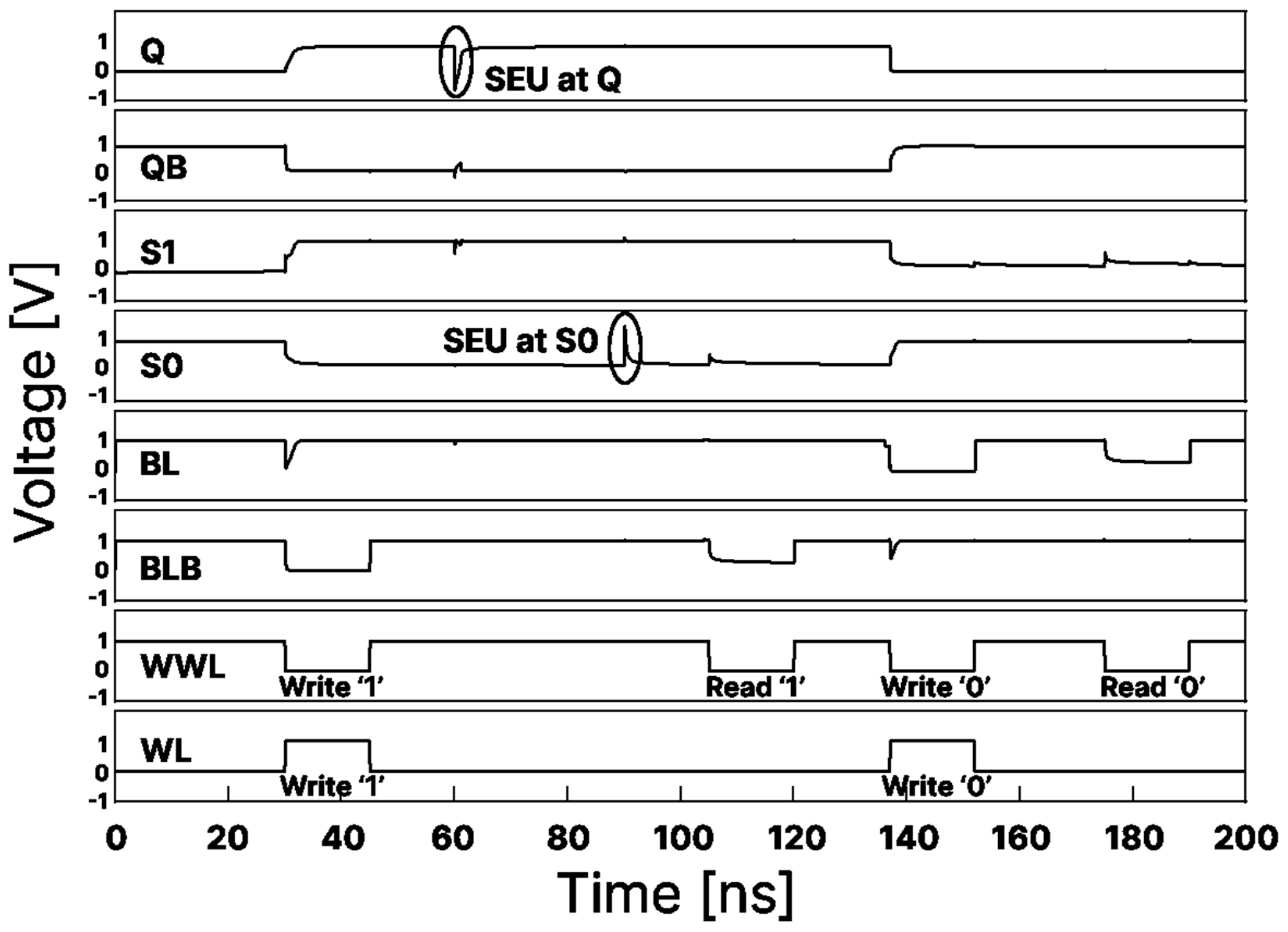
Figure 2 presents its corresponding layout. The proposed 16T cell’s bit-cell structure contains four nodes. Among them, two nodes, Q and QB, are storage nodes, while the others, S1 and S0, are internal nodes. The access transistors are denoted as N1, N8, P1, and P8. Transistors P1 and P8 are controlled by the word line (WL), whereas transistors N1 and N8 are regulated by the write word line (WWL). When the WL/WWL are set to GND/VDD, the access transistors connect the nodes to their respective bit lines. Transistors N8 and P8 connect nodes Q and S1 to BL, while transistors N1 and P1 connect nodes QB and S0 to BLB. When the stored bit is ‘1’, nodes Q, QB, S1, and S0 have logical states of ‘1’, ‘0’, ‘1’, and ‘0’, respectively. This paper explains all operations by assuming the proposed cell is in the initial state of ‘1’.
(1) Hold Operation: The WL/WWL are set to VDD/GND in the hold operation, ensuring that all access transistors connected to the nodes remain off. For the assumed initial state of ‘1’, transistors N2, N4, N5, P3, P5, and P6 are turned on while the other transistors are turned off. Thus, nodes Q and S1 can retain their initial state of ‘1’ because they are connected to VDD through the paths ‘Q-N5-P5-VDD’ and ‘S1-P6-VDD’, respectively. Similarly, nodes QB and S0 can retain their initial state of ‘0’ through the paths ‘QB-N4-GND’ and ‘S0-P3-N2-GND’, respectively. This ensures the stable operation of the cell in the initial state.
(2) Read Operation: Bit lines BL and BLB are pre-charged to VDD for the read operation. Subsequently, the WL/WWL are set to GND/GND, ensuring the storage nodes Q and QB are isolated from the bit lines. From the assumed initial state, BLB discharges through the pull-down transistors P3 and N2, while BL remains at the pre-charged VDD value, as P7 and N7 are off. Once the voltage difference between BL and BLB reaches approximately 50 mV, the sense amplifier performs the read operation [
3].
(3) Write Operation: To convert the stored data from ‘1’ to ‘0’ within the cell, bit lines BL and BLB are pre-discharged or pre-charged to GND and VDD, respectively. The WL/WWL are set to GND/VDD, ensuring that all access transistors connected to the nodes are in the on state. The voltages at QB and S0 rise through access transistors N1 and P1, respectively. As the voltages of QB and S0 increase, the pull-up paths to Q and S1 weaken, facilitating the rapid discharge of Q. Once the voltage of Q drops sufficiently, the pull-down transistors N2 and N4, connected to QB and S0, turn off, thereby speeding up the charging process of QB and S0. Thus, the states of all nodes can be changed to the desired values using their respective access transistors. Note that synchronously changing the values of both the storage and internal nodes with both of their respective access transistors enhances the speed of the cell’s write operation.
2.2. Soft-Error Recovery Analysis
This subsection explains the characteristics of the proposed cell. A node is considered sensitive when it is affected by SEUs [
3]. Generally, PMOS and NMOS transistors are known to induce positive and negative transient pulses, respectively [
16]. For instance, in the case of PMOS, positive transient pulses can occur during transitions from ‘0’ to ‘1’ or from ‘1’ to ‘1’. However, if the datum stored at the node is ‘1’, the node retains its state as ‘1’, even if a positive transient pulse is induced. Therefore, for PMOS, only the positive transient pulse during the transition from ‘0’ to ‘1’ needs to be considered. In contrast, in the case of NMOS, negative transient pulses can occur during transitions from ‘1’ to ‘0’ or from ‘0’ to ‘0’. However, if the datum stored at the node is ‘0’, the node retains its state as ‘0’, even if a negative transient pulse is induced. Thus, for NMOS, only the negative transient pulse during the transition from ‘0’ to ‘0’ needs to be considered. In summary, nodes storing ‘1’ and surrounded by PMOS transistors and nodes storing ‘0’ and surrounded by NMOS transistors can be regarded as insensitive because only positive transient pulses and negative transient pulses, respectively, can occur in these nodes. Given the initial state of ‘1’ for the proposed 16T cell, the storage node QB starts with a value of ‘0’ and is surrounded exclusively by NMOS transistors. Hence, the only possible transient state when an SEU occurs is ‘0’→‘0’. Similarly, the internal node S1 has an initial value of ‘1’ and is surrounded only by PMOS transistors, resulting in the possible transient state of ‘1’→‘1’ during an SEU. Therefore, for the assumed initial state, nodes QB and S1 can be considered insensitive, while Q and S0 are sensitive nodes. Waveforms for soft-error recovery and the fundamental hold/read/write operations of the proposed RHSP16T cell are shown in
Figure 3.
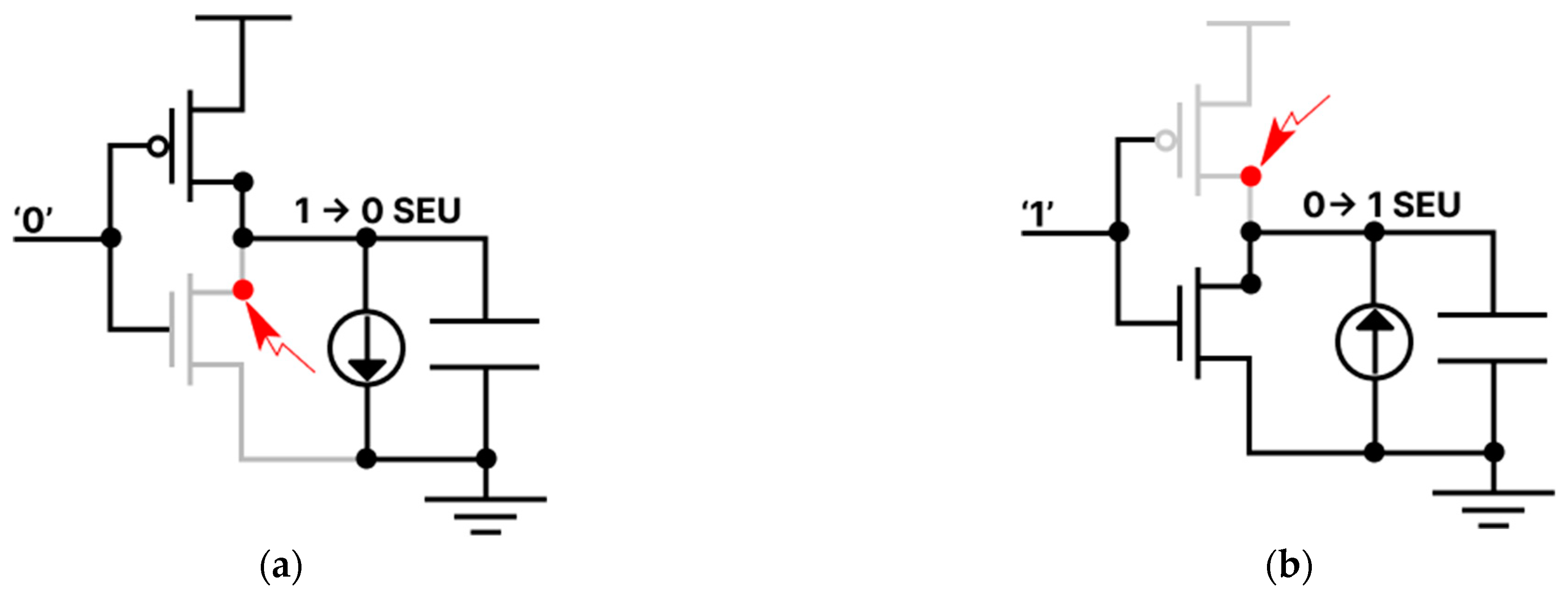
(1) SEU at node Q: When an SEU occurs at node Q, the state of Q changes from ‘1’ to ‘0’. This transition turns off transistor N4 and activates transistors P4 and P7. As a result, transistors P2 and N3 will remain off, which leads to nodes QB and S0 entering a high-impedance state. In the high-impedance state, they are disconnected from both the pull-up and pull-down paths, typically meaning their state remains unaffected [
3]. Therefore, nodes QB and S0 will retain their initial state of ‘0’. Since QB and S0 maintain their initial state, transistor N7 will stay off while transistor P6 will remain on. This setup allows node S1 to be pulled up to VDD through the path ‘S1-P6-VDD’, maintaining its initial state of ‘1’. With nodes QB, S0, and S1 remaining stable in their initial states, node Q, affected by the SEU, can be restored to its initial state of ‘1’ by being pulled up to VDD through the path ’Q-N5-P5-VDD’.
(2) SEU at node S0: When an SEU flips S0 from ‘0’ to ‘1’, it causes transistor N3 to turn on and transistor P6 to turn off. However, since transistors P7 and N7 remain off, node S1 will enter a high-impedance state, allowing it to maintain its initial value of ‘1’. As node S1 holds its initial state, transistor N5 remains on, which allows node Q to be pulled up to VDD through the path ‘Q-N5-P5-VDD’, thus retaining its initial state of ‘1’. For node QB, although the activation of transistor N3 will occur due to the flip of S0, the initial state of node Q will keep transistor P4 off, disconnecting QB from the pull-up path. Therefore, node QB will maintain its initial state of ‘0’ as it is pulled down to GND through the path ‘QB-N4-GND’. Since nodes Q, QB, and S1 are not directly affected by the SEU and retain their initial states, node S0, impacted by the SEU, can be restored to its initial state of ‘0’ by being pulled down to GND through the path ’S0-P3-N2-GND’.
(3) SEMNU at node pair Q-S0: When sufficient charge accumulates at the node pair Q-S0, it can cause the cell to flip to a different state. The feedback mechanism between the nodes prevents recovery to the initial state. However, charge sharing between transistors can be prevented by keeping a minimum spacing of 1.62 μm between PMOS transistors and 0.6 μm between PMOS and NMOS transistors [
4]. As shown in
Figure 2, the layout of the proposed RHSP16T cell maintains a spacing of 4.175 μm between Q and S0, thereby preventing SEMNUs at this node pair.
3. Simulation Results and Analysis
This section presents the simulation results for the RHSP16T cell. The performance of the proposed RHSP16T cell was evaluated using various design metrics with 90 nm CMOS technology, and the bsim3V3 model was used for the transistors. To demonstrate the superiority of the RHSP16T cell, the simulated design metrics were compared with those of the QUCCE12T, WE-QUATRO, RHBD10T, RHD12T, and RSP14T cells. To enhance the read stability of the RHSP16T cell, the widths of transistors N2, N7, P3, and P7 were set to 1.7 times that of the access transistors N1 and P1. For improved write speed and stability, the widths of transistors P6 and P2 were set to 0.34 times those of their respective access transistors, while the widths of transistors N3, N5, P4, and P5 were set to 0.5 times those of their respective access transistors. Additionally, the transistor sizes specified in the respective papers were used for simulating the other comparison cells.
3.1. Read and Write Access Time Comparison
Read access time (RAT) can evaluated with the time interval from when the voltage of the WL reaches 50% of the supply voltage VDD to when the voltage difference between the two bit lines, BL and BLB, reaches 50 mV [
17]. It is shown in
Figure 4a. Generally, read access time heavily depends on the read current through the access and pull-down transistors and the bit-line capacitance [
18]. The excessive use of access transistors results in higher bit-line capacitance than a single access transistor, leading to longer read access times. Furthermore, a higher cell ratio (CR), representing the ratio of the pull-down transistor to the access transistor, tends to result in shorter read access times [
19].
Table 1 shows that the proposed RHSP16T structure has the longest read access time among all the cells. During the read operation in the RHSP16T, only the access transistor connected to the internal node was activated, resulting in higher bit-line capacitance than in the cells using a single access transistor. Additionally, the access transistor activated during the read operation was a PMOS transistor with a lower charge mobility than NMOS transistors. This contributed to the longer read access time for the RHSP16T cell during the read operations.
Write access time (WAT) can evaluated with the time interval from when the WL voltage reaches 50% of the supply voltage VDD to when the storage nodes Q and QB intersect [
18]. It is shown in
Figure 4b. According to
Table 1, the WAT of the proposed RHSP16T is 86.71%, 95.56%, 61.64%, 62.65%, and 63.29% of those of QUCCE12T, WE-QUATRO, RHBD10T, RHD12T, and RSP14T, respectively, making it the shortest among all the compared cells. Several factors contribute to this. Firstly, in the proposed RHSP16T, both access transistors connected to each bit line were activated during the write operation, allowing simultaneous flipping of the storage node and internal node values. This process accelerated the write operation compared to cells using a single access transistor [
18]. Moreover, the RHSP16T has the lowest pull-up ratios of 0.34 and 0.5 for the two pairs of access transistors. A lower pull-up ratio ensures that the pull-down force exerted by the access transistors discharging to a pre-discharged bit line at ‘0’ was stronger than the pull-up force of the pull-up transistors pulling the node to ‘1’, resulting in a shorter WAT. Furthermore, the RHSP16T uses an NMOS pull-up transistor, which has a weak ‘1’ characteristic, for the storage nodes, making it easier for the access transistors to discharge the weak ‘1’. Consequently, the proposed RHSP16T achieved the shortest WAT, allowing for faster writing of new signals.
3.2. Read and Write Stability Comparison
Read stability can be estimated through the read static noise margin (RSNM) [
20]. Typically, the static noise margin represents the maximum DC noise voltage that each storage node can withstand before a read upset occurs, and it is obtained by the length of the largest square side in a butterfly curve [
21,
22]. During the read operation, the storage node holding ‘0’ was connected to the bit line, which was pre-charged to the VDD. As a result, the read current flowing from the bit line to the ‘0’ storage node could induce voltage on the node, potentially flipping the stored data [
18]. Therefore, stable read operations are crucial for the functionality of SRAM cells.
Table 1 shows a comparison of the RSNM values of various SRAM cells, and
Figure 5 illustrates the RSNM curves for different cells. As shown in
Table 1, the RSNM of the proposed RHSP16T cell is 257.1%, 210.7%, 158.5%, 174.7%, and 179.9% those of QUCCE12T, WE-QUATRO, RHBD10T, RHD12T, and RSP14T, respectively, making RHSP16T the cell with the highest RSNM among all compared cells. This enhanced RSNM was due to the read-decoupled characteristics of the proposed RHSP16T cell. During the read operation, only one pair of access transistors out of the two pairs was activated, and only the internal nodes were connected to the bit lines. This configuration prevented the storage nodes Q and QB from being directly affected by noise. Moreover, the appropriate CR setting of 1.7 for the proposed 16T cell resulted in a lower voltage at the internal node S0 storing ‘0’. Therefore, RHSP16T achieved a high RSNM value, indicating that it provides stable read operations.
Recent research suggests that word-line write-trip voltage (WWTV) provides a more dependable assessment of an SRAM cell’s write capability than the write static noise margin (WSNM) [
3]. WWTV is determined by the difference between the word line voltage when the storage nodes Q and QB intersect and the supply voltage VDD when the word line is activated. Consequently, cells with longer write access times need more time to modify the stored data, which results in a higher voltage increase at the word line when Q and QB intersect. As shown in
Table 1, the WWTV of the proposed RHSP16T cell is 121.1%, 122.2%, 146.7%, 124.4%, and 124.4% of those of QUCCE12T, WE-QUATRO, RHBD10T, RHD12T, and RSP14T, respectively. The proposed RHSP16T cell has the highest WWTV value among all compared cells, indicating that RHSP16T can perform very stable write operations.
3.3. Power-Consumption Comparison
Since SRAM cells predominantly operate in hold mode, the power consumed during the hold operation, referred to as hold power, represents a considerable portion of the total power consumption of an SRAM cell [
23]. This power consumption primarily arises from bit-line leakage and the leakage associated with the inverters used in the SRAM cell. Due to carrier mobility, NMOS transistors generate more leakage power than PMOS transistors through the bit lines. Furthermore, in the internal inverter structure, higher resistance in the pull-up and pull-down paths of the transistors leads to lower leakage power.
Table 1 shows that the leakage power of the proposed RHSP16T cell is 101.9%, 97.08%, 78.04%, 73.79%, and 73.92% those of QUCCE12T, WE-QUATRO, RHBD10T, RHD12T, and RSP14T, respectively. The proposed 16T SRAM structure, despite having two pairs of access transistors, reduces power consumption by utilizing PMOS transistors for one pair of access transistors. Additionally, by implementing a stacking structure for the internal transistors, it demonstrated lower power consumption compared with most other SRAM cells [
23].
3.4. Soft-Error Robustness Verification and Comparison
In this section, the robustness of the proposed RHSP16T cell against soft errors is evaluated through circuit-level simulations. As shown in
Figure 6, a double exponential current source was used to charge the sensitive nodes of the cell, simulating the charge-collection phenomenon that occurs when high-energy particles strike circuit nodes. The double exponential current source used to evaluate the robustness against soft errors was determined by the following equation [
24]:
In the equation,
represents the peak current of the current pulse,
tα is the initial ion-track setup time constant, and
tβ is the collection time. In this study,
tα and
tβ were set to 200 ps and 50 ps, respectively, for the experiments. The critical charge,
, is the minimum charge required to flip the cell’s value when the sensitive node is affected by a single-event upset (SEU). Typically, different amplitudes of
are injected into sensitive nodes to estimate this, allowing for the determination of the minimum
and the critical time,
, at which the cell’s value flips. The critical charge,
, can then be calculated using the following equation:
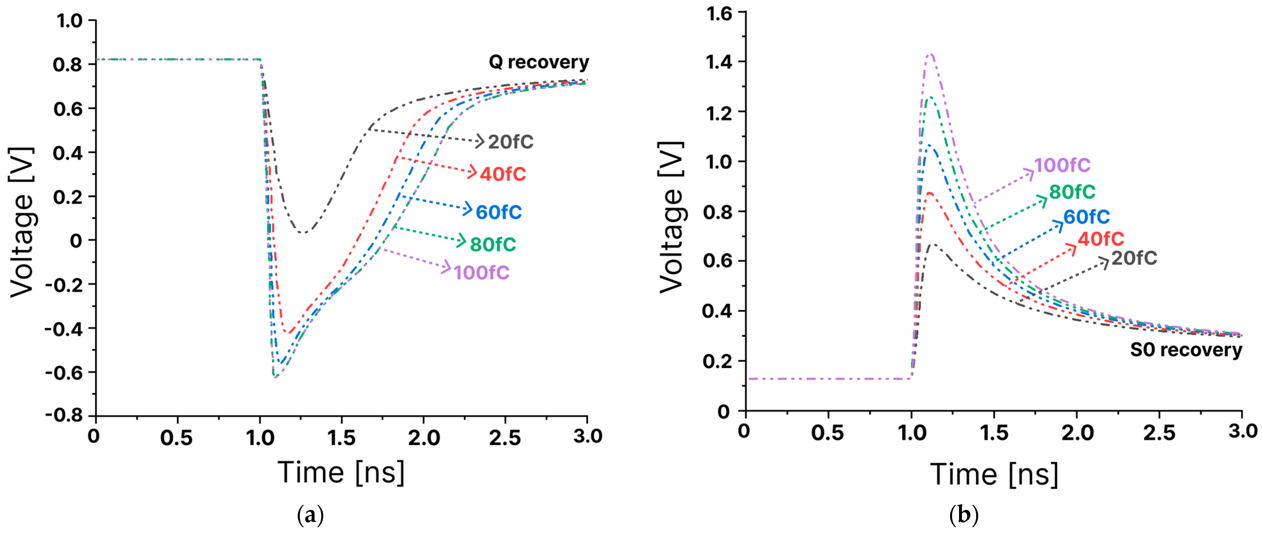
The
values for all cells are presented in
Table 1. Additionally, the recovery simulation for sensitive nodes
Q and S0, assuming the proposed RHSP16T cell initially stores a ‘1’, is shown in
Figure 7.
Figure 7 demonstrates that RHSP16T can be successfully restored from SEUs at levels above 100 fC. Furthermore, as described in
Section 2, RHSP16T avoided charge-sharing effects between node pairs
Q and S0 by appropriately spacing the sensitive nodes
Q and S0 in the layout. Therefore, the radiation-hardened RHSP16T cell exhibited strong robustness and reliability.
3.5. Electric Quality Metric Comparison
Critical charge,
, effectively indicates SRAM cell performance in space. However, the performance of SRAM cells is influenced by multiple factors beyond
. Parameters such as RAT, WAT, RSNM, WWTV, power consumption, and area are also crucial for SRAM cell operation. Each of these parameters has trade-offs; improving one may deteriorate another. Therefore, instead of comparing cell performance based on each parameter individually, a comprehensive performance metric that considers all factors affecting SRAM cell operation is required. The Electric Quality Metric (
EQM) represents the overall performance of an SRAM cell and is given by the following formula [
3]:
To compare the
EQM values of the proposed RHSP16T cell and all comparison cells, the relative
EQM /
) values for all the cells are shown on a logarithmic scale in
Figure 8. As shown in
Figure 8, the proposed RHSP16T cell exhibited the highest
EQM value, indicating its superior performance compared with the other cells.
4. Conclusions
In this paper, we propose a radiation-hardened SRAM cell, named RHSP16T, designed for space applications to achieve immunity against soft errors while demonstrating optimized performance in terms of stability and power consumption. The proposed RHSP16T cell designates two out of its four nodes as sensitive nodes, which can recover from all SEUs induced at these sensitive nodes. Furthermore, the RHSP16T cell incorporates layout-level techniques to avoid charge-sharing effects at sensitive node pairs, thereby ensuring immunity to SEMNUs. Simulation results indicate that the proposed RHSP16T cell outperforms other comparative cells across various design metrics fundamental to SRAM operations, including write access time, write stability, read stability, and power efficiency. Additionally, the EQM evaluation further verified the overall superior performance of the RHSP16T cell. However, the proposed design has certain limitations, including a slightly increased read access time and a minor increase in area. Therefore, future research should focus on optimizing the read access time and area while preserving the cell’s stability and power efficiency. In summary, the proposed RHSP16T cell provides immunity to soft errors, high read and write stability, and enhanced data reliability, making it suitable for the space industry, where reliable data processing over extended periods with relatively low power consumption is essential.


