Article

Integrated Deep Ultraviolet Doublet Metalens for Projection Imaging

Center for Advanced Optoelectronic Functional Materials Research, Key Laboratory of UV Light-Emitting Materials, Technology of Ministry of Education, College of Physics, Northeast Normal University, Changchun 130024, China
*
Author to whom correspondence should be addressed.
Appl. Sci. 2024, 14(3), 1316; https://doi.org/10.3390/app14031316
Submission received: 20 December 2023 / Revised: 26 January 2024 / Accepted: 1 February 2024 / Published: 5 February 2024
(This article belongs to the Special Issue Metamaterials, Quantum and Nanophotonics in the Third Millennium)

Abstract

:
Metalenses, with their unique modulation of light, are in great demand for many potential applications. As a proof-of-principle demonstration, we focus on designing SiO2 metalenses that operate in the deep ultraviolet region, specifically around 193 nm. Based on the deep ultraviolet metalens proposed in this paper, an integrated deep ultraviolet doublet metalens is further offered. When the incident light is a plane wave with a wavelength of 193 nm, the integrated doublet metalens can reduce the beam size by a factor of 4:1, and the emitted light is flat. The integrated doublet metalens can project the reticle image proportionally, making the projection image clear. The integrated doublet metalens has the best imaging effect at the propagation distance of 2 μm and can tolerate ±3 degrees of incident angle deviation. Our findings establish general and systematic strategies to guide the design of traditional optical lens arrays with excellent integrated doublet metalenses and pave the way for enhanced optical performance in the application of large-relative-aperture deep ultraviolet detection, deep ultraviolet microscope systems, laser beam combining systems, deep ultraviolet lithography systems, etc.

1. Introduction

In recent years, the study of metasurfaces has become a major topic due to the unique electromagnetic modulation properties of the sub-wavelength micro-nano structure in micro-nano optics [1,2,3,4,5,6]. There are many research directions regarding metasurfaces, including holograms [7,8,9], beam shaping [10,11,12], sensing [13,14], polarization control [15,16,17], absorbers [18,19,20,21,22], biosensing [23,24], and metalenses [25,26,27,28,29,30,31,32,33]. Lenses are crucial optical components in various applications, including security, automotives, lasers, digital cameras, and optical instruments. Metalenses represent a popular research direction as they can control light waves through arrays of micro-nano structures. They have the advantages of being ultra-light, ultra-thin, easy to integrate, etc., and are expected to open up a new path for micro and micro-nano optical imaging and optoelectronic equipment. The study of metalenses in the visible [26] and near-infrared [27] regions has developed well, and single-wavelength [28,29], multi-wavelength [30], and achromatic metalenses [31,32,33] in visible wavelengths have been realized. However, studies on metalenses [34,35,36] in the deep UV band are still scarce. Recently, high-bandgap materials such as HfO2 [37] and TiO2 [38] have been introduced as compelling material platforms for UV-range applications. There are also many excellent research results on multilayer metasurfaces [39,40].
There are many application scenarios for deep ultraviolet systems [41,42,43], such as large-relative-aperture deep ultraviolet detection [43,44,45], deep ultraviolet microscope systems [41,46,47], laser beam combining systems [48,49], deep ultraviolet lithography systems [50], etc. Among them, the deep ultraviolet large-relative-aperture warning optical system [43,44,45] requires the optical system to have a large field of view, large relative aperture, simple structure, and small light energy loss. This requires a combination of spherical mirrors, diffractive elements, and aspheric mirrors, and the system is difficult and costly to handle. The laser beam combining system [48,49] achieves laser output with high power and power density while maintaining high beam quality. By spatially rearranging the output beam of each light-emitting unit or refracting and reflecting the optical path, the output beam of each light-emitting unit can be combined into a beam close to a single light-emitting unit, improving the beam quality and output density. The projection lithography objective lens [50] is also an essential deep ultraviolet system; it is the core component of the projection lithography machine. Its performance determines the image transfer capability of the deep ultraviolet lithography machine. The projection objective lens group often requires a complex lens combination of nearly 30 lenses and more than a dozen movable lenses with sub-nanometer machining accuracy. The deep ultraviolet metalens based on the metasurface has a powerful wavefront control capability. It can use as few lens combinations as possible to achieve the functions of a traditional lens group.
In this paper, we propose an integrated deep ultraviolet all-dielectric doublet metalens to solve the problem of the complex structure of the existing traditional deep ultraviolet system. This can be used in a projection deep ultraviolet lithography machine system, laser beam combining systems, and deep ultraviolet detection. Two metalenses are designed on two parallel surfaces on the SiO2 substrate, respectively, with the same numerical aperture and focal length ratio of 4:1. The centers of the two metalenses are aligned and spaced at the sum of the two focal lengths. The beam reduction of the parallel deep ultraviolet light is realized through the design optimization of each metalens. We analyze the efficiency of the integrated doublet metalens, and the light intensity per unit area of the emitted light is 7.39 times the intensity of the incident light unit area. Projection imaging is realized for the reticle placed in the integrated doublet metalens under the incidence of parallel light. The doublet metalens realizes the function of projection imaging through an integrated array. We can adjust the size and focal length of the two metalenses according to the required imaging ratio to obtain a pattern consistent with the corresponding ratio of the propagation distance. It has the advantages of being ultra-light, ultra-thin, and easy to integrate and opens up a new path for deep ultraviolet lithography, micro-nano optical imaging, and optoelectronic equipment. Compared with the traditional deep ultraviolet lens group, this design has the advantages of a small volume, simple system structure, stable system, etc.

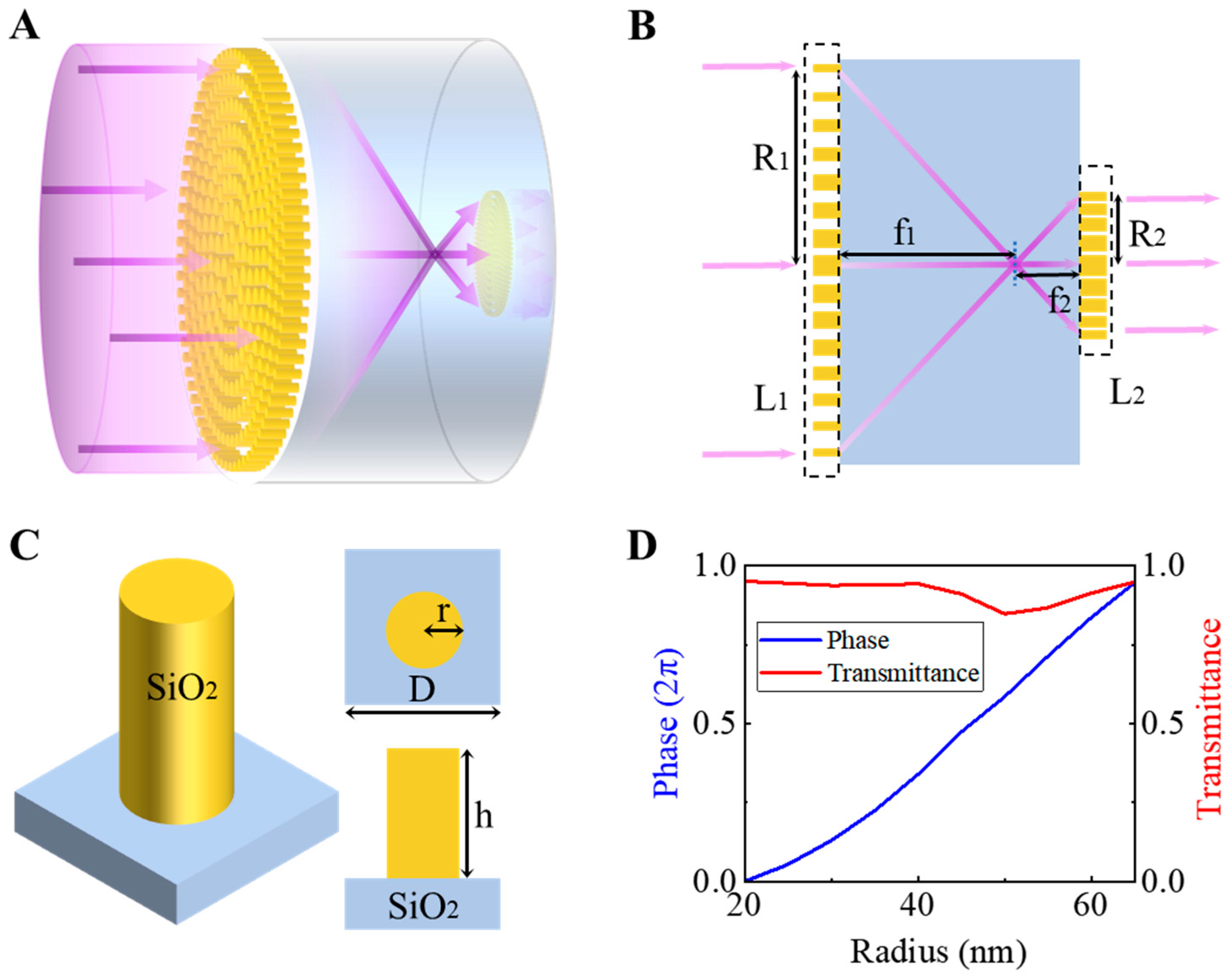
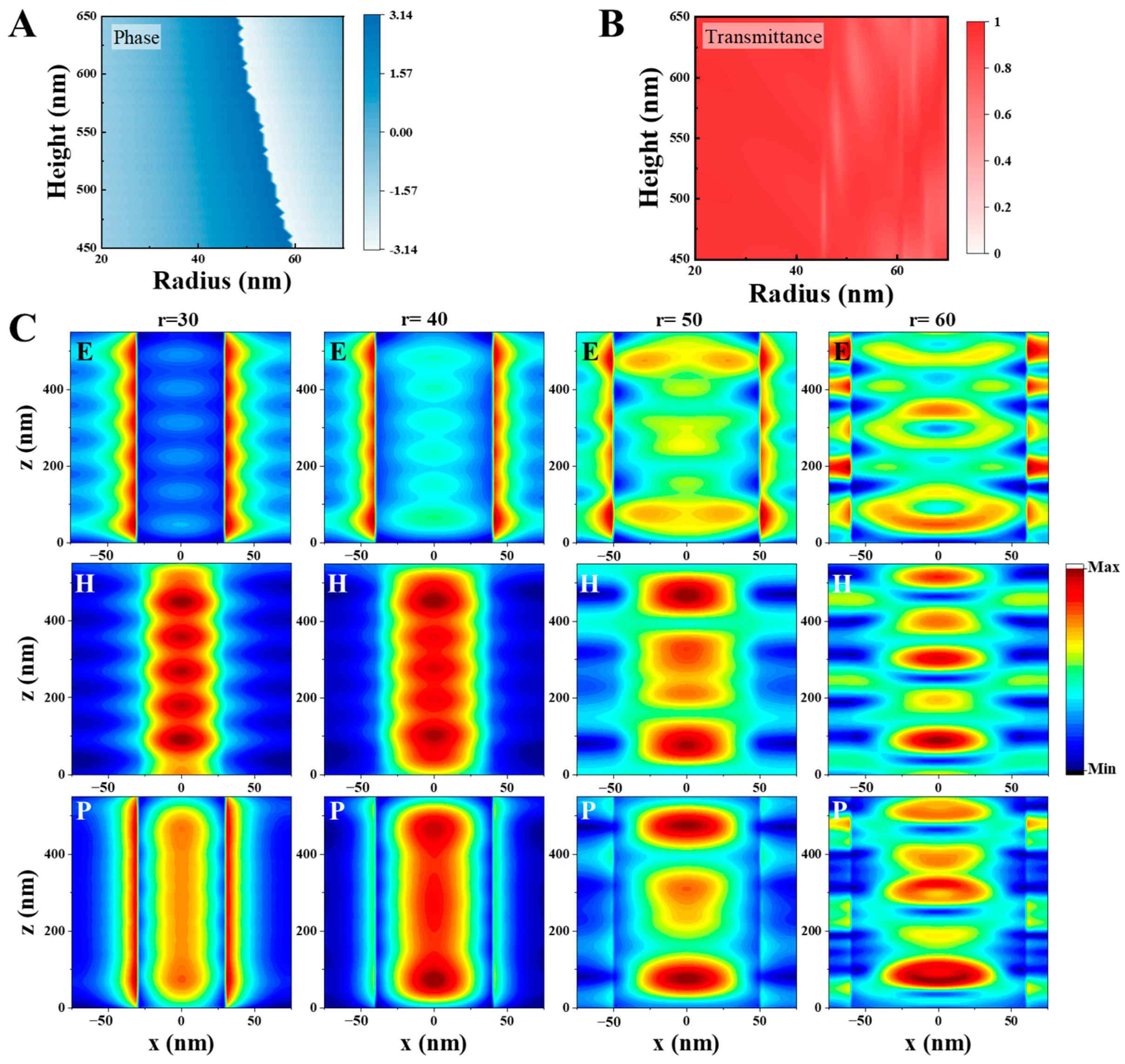
2. Materials and Methods

The principle of the metalens is shown in Figure 1. The propagation phase structure is used to design a deep ultraviolet all-dielectric metalens. The unit structure of the SiO2 cylinder is placed on the SiO2 substrate. SiO2 [51] has higher transmission efficiency and lower absorption in the deep ultraviolet band, which can improve the performance of the metalens. It is common for a cylinder [52,53,54,55] to be used as the unit structure for a metalens. By adjusting the geometric parameters, such as the radius and height of the cylinder, phase coverage of 2π can be obtained to achieve the arbitrary control of the wavefront.
The finite difference time domain (FDTD) method is used to simulate the phase control element and the phase and intensity of the metalens. Theoretical simulations are conducted on the transmittance and phase of the phase-regulating unit, as well as on the transmittance and projection intensity of the metalens and doublet metalens. The simulation of the element structure uses periodic boundary conditions along the x and y axes and a perfect matching layer along the z axis. The refractive index of SiO2 comes from the Palik manual, emitting plane waves from the bottom of the metasurface.
The parameters of the unit structure are shown in Figure 2. By adjusting the geometric parameters such as the unit size and height, 2π phase coverage can be obtained, and arbitrary control of the light field can be achieved. To realize the phase control under the design wavelength λ = 193 nm, we choose the SiO2 material with high transmittance as the substrate and unit structure pillar. We select the cylindrical structure to adjust and scan its radius and height. Based on observations, it can be seen that within a radius of 20–70 nm, the ability to adjust the phase becomes more robust with an increase in height. Therefore, selecting a height that offers higher transmittance overall is advisable. After careful consideration, choosing a height of 550 nm and a radius between 20 and 65 nm is recommended. The phase delay covers a 2π interval, the overall transmittance is above 84%, and the average transmittance reaches 92%. In the design of ultraviolet metalenses [56,57,58,59], the element structure’s amplitude and phase control results are quite acceptable. The full-wave simulations (E, H, and P) of meta-units with different radii (30, 40, 50, and 60 nm) are shown in Figure 2C.
In this paper, the propagation phase is controlled by changing the radius of the SiO2 cylinder. To achieve focus, the phase of the deep ultraviolet all-dielectric metalens needs to satisfy the following equations:
Φ = 2 π λ f f 2 + x 2 + y 2
Among them, λ is the wavelength of the incident light, f is the focal length, and (x, y) is the position coordinate on the transparent substrate. When the exit light interface is located in a medium with a refractive index of n, the phase profile must satisfy the following:
Φ = n × 2 π λ f f 2 + x 2 + y 2
The phase shift introduced by the unit structure can be expressed as
Φ = 2 π λ n H
where H is the unit structure height.
To improve the focusing effect, we perform aspherical aberration [60] processing on both metalenses, namely
Φ = n × 4 π λ 2 f x 2 + y 2 + 4 f 2
In Figure 3 below, Figure 3A is a schematic diagram of the focusing of a single metalens, and Figure 3B,C is the phase profile curves required by metalens L1 and L2, respectively, according to Equation (4). We can observe that the aspherical phase profile is basically the same as the conventional one. The phase profile coincides with the lens’s center. With an increase in r, the phase profile of the aspherical metalens changes faster than the conventional one.
We create two metalenses with the same numerical aperture, and the focusing effect is satisfactory compared to the proposed UV metalens [56,57,58,59]. In Figure 4, the focusing effect of the two metalenses is shown, where Figure 4A–C show the focusing effect of metalens L1, and Figure 4D–F show the focusing effect of metalens L2. As depicted in Figure 4A, the focal length of metalens L1 is 6 μm, which is consistent with our design focal length. The focusing effect of the focal plane is shown in Figure 4B, and the intensity at the radial position on the focal plane is shown in Figure 4C. The FWHM is 0.17 μm, and the central peak area accounts for 93.76%. As depicted in Figure 4D, the focal length of metalens L2 is 1.5 μm, which is consistent with our design focal length. The focusing effect of the focal plane is shown in Figure 4E, and the intensity at the radial position on the focal plane is shown in Figure 4F. The focus half-width is 0.158 μm, and the central peak area accounts for 94.22%.
To realize the beam reduction function, two metalenses with the same NA are designed, namely
R 1 f 1 = R 2 f 2
R1 and f1 are the radius and design focal length of metalens L1, and R2 and f2 are the radius and design focal length of metalens L2, respectively, which are expressed explicitly as
R 1 : R 2 = 4 : 1
f : f 2 = 4 : 1
Thus far, we have obtained two metalenses, L1 and L2, with the same numerical aperture and a diameter ratio of 4:1. They have an excellent focusing effect at the design wavelength of 193 nm. An integrated doublet metalens is further designed to achieve the perfect beam reduction of parallel light with a simple structure. The sum of the focal lengths of the two metalenses is ftotal = f1 + f2, which is the same thickness as the SiO2 substrate, as shown in Figure 1B.

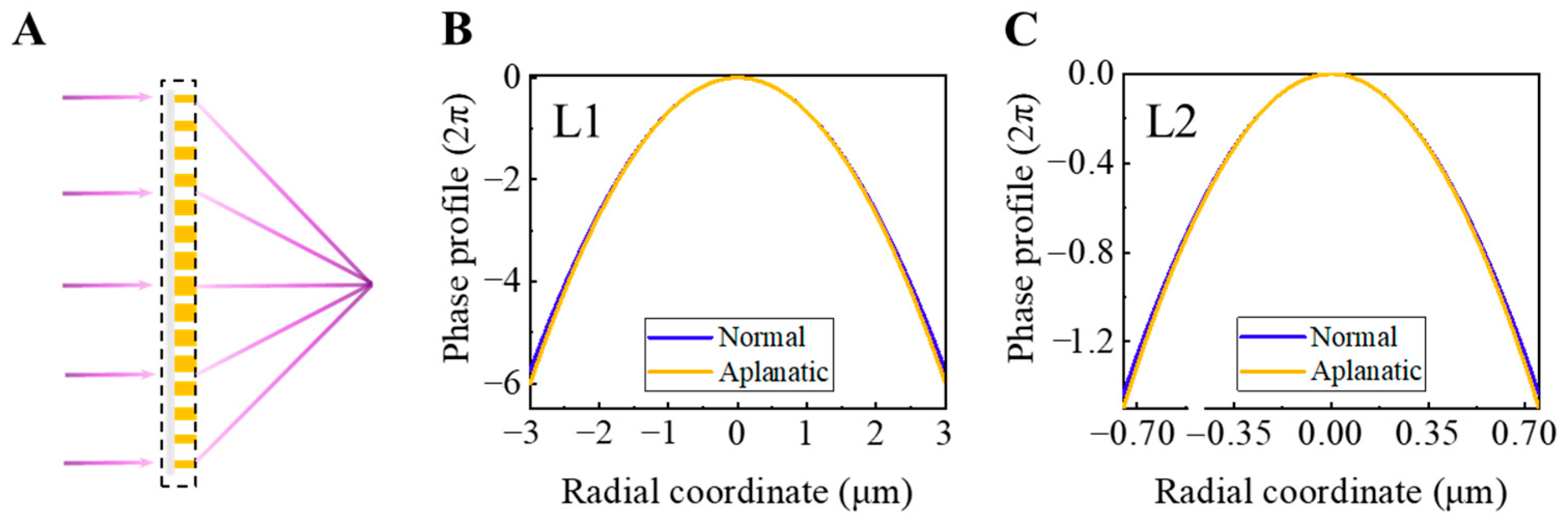
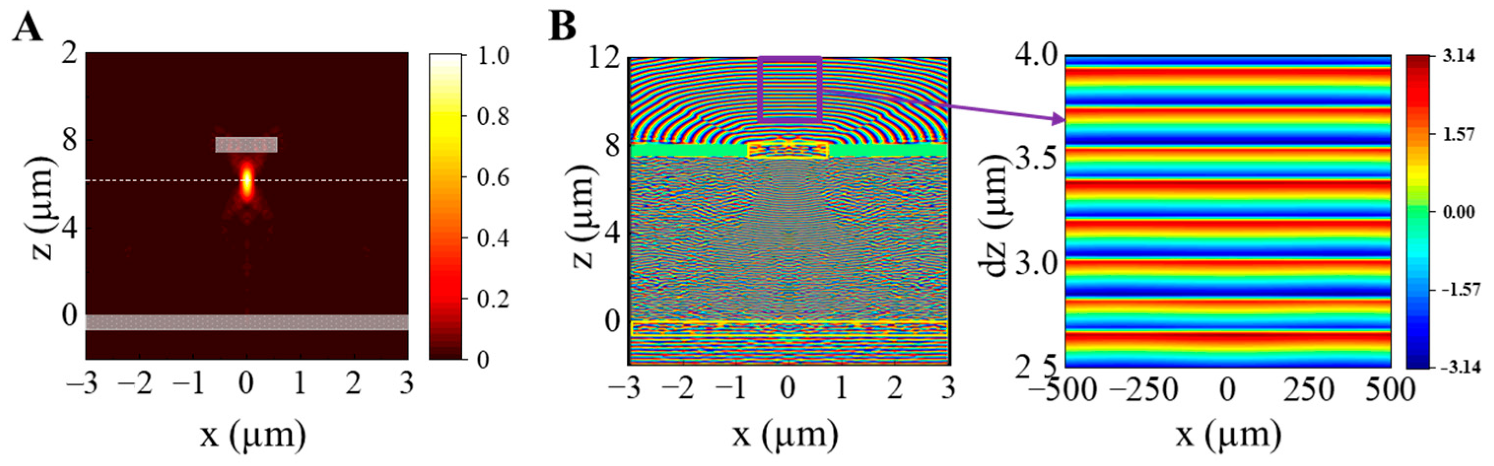
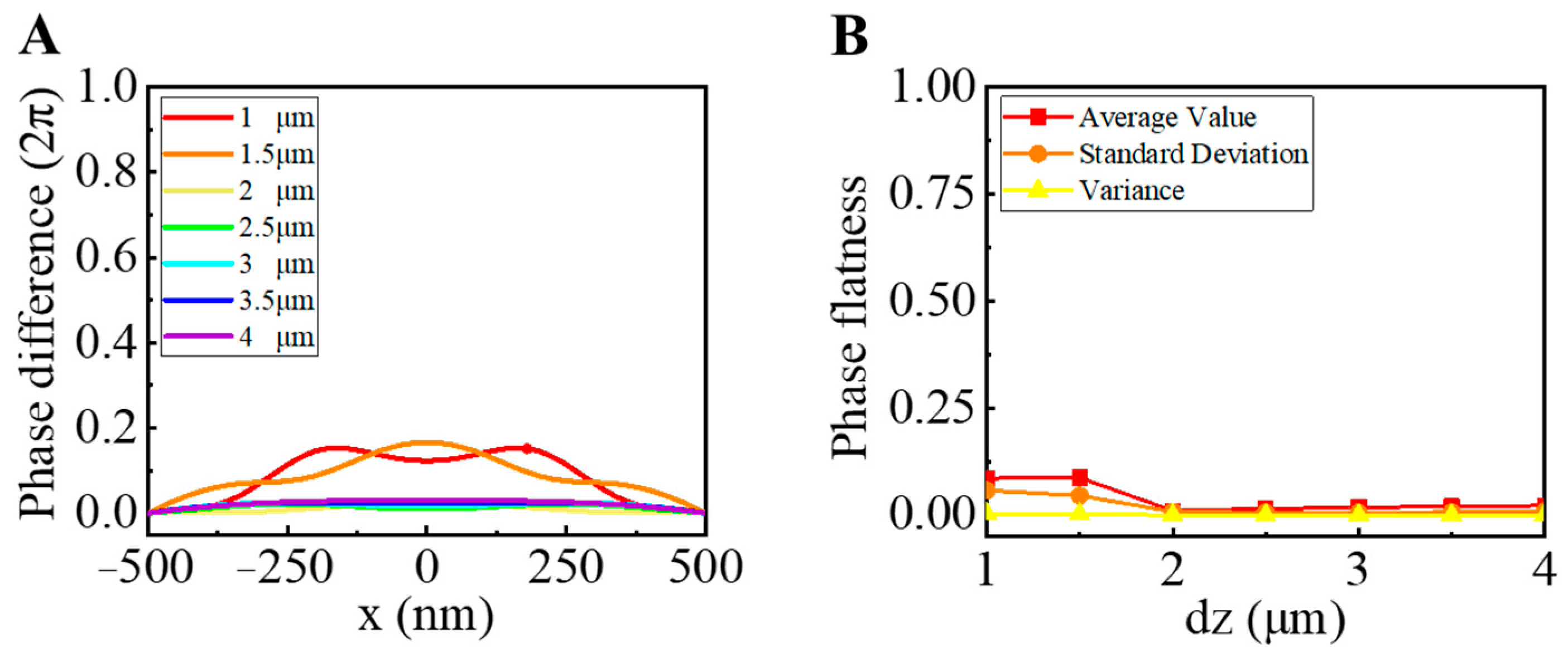
Analysis of Flatness of Outgoing Light
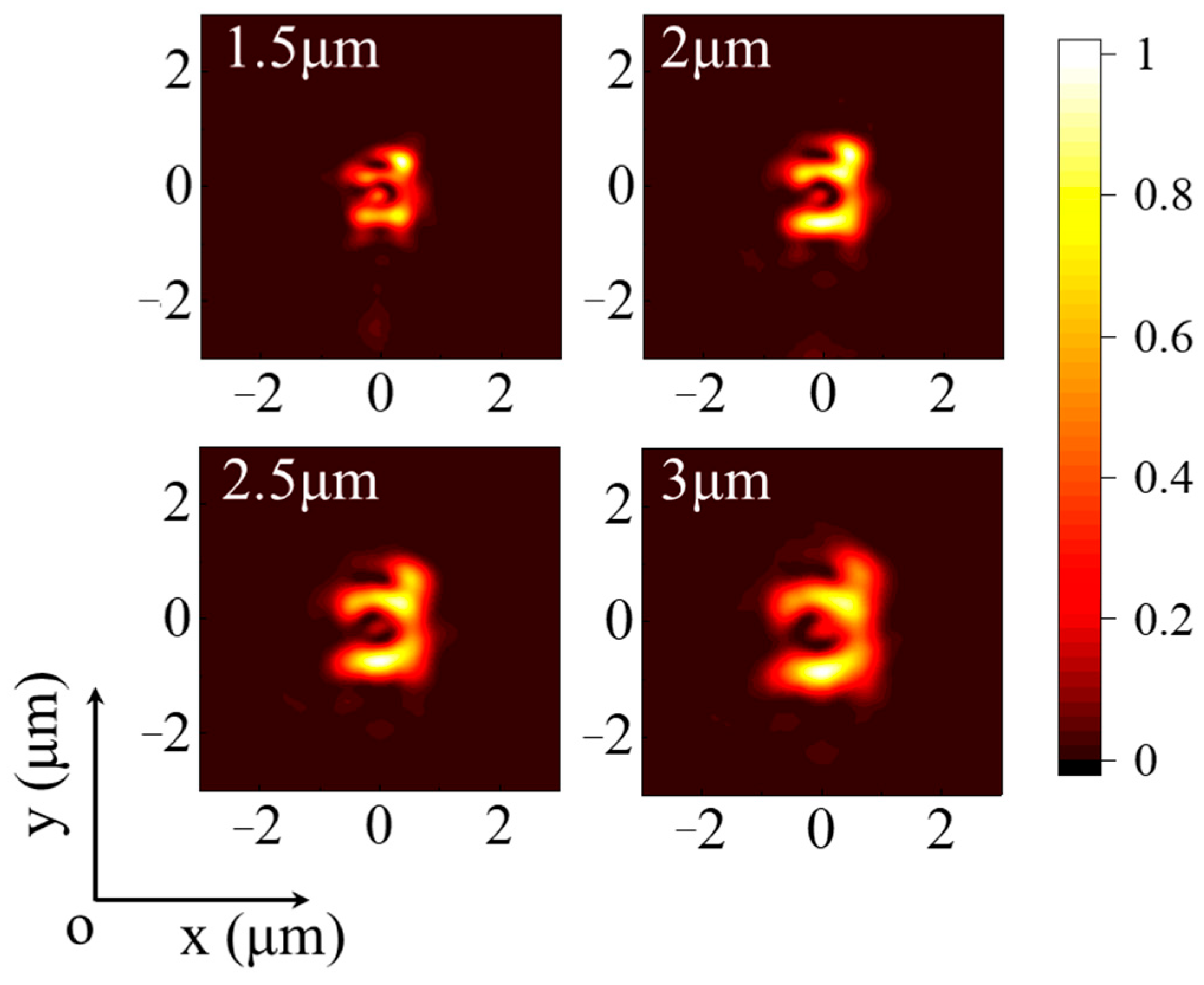
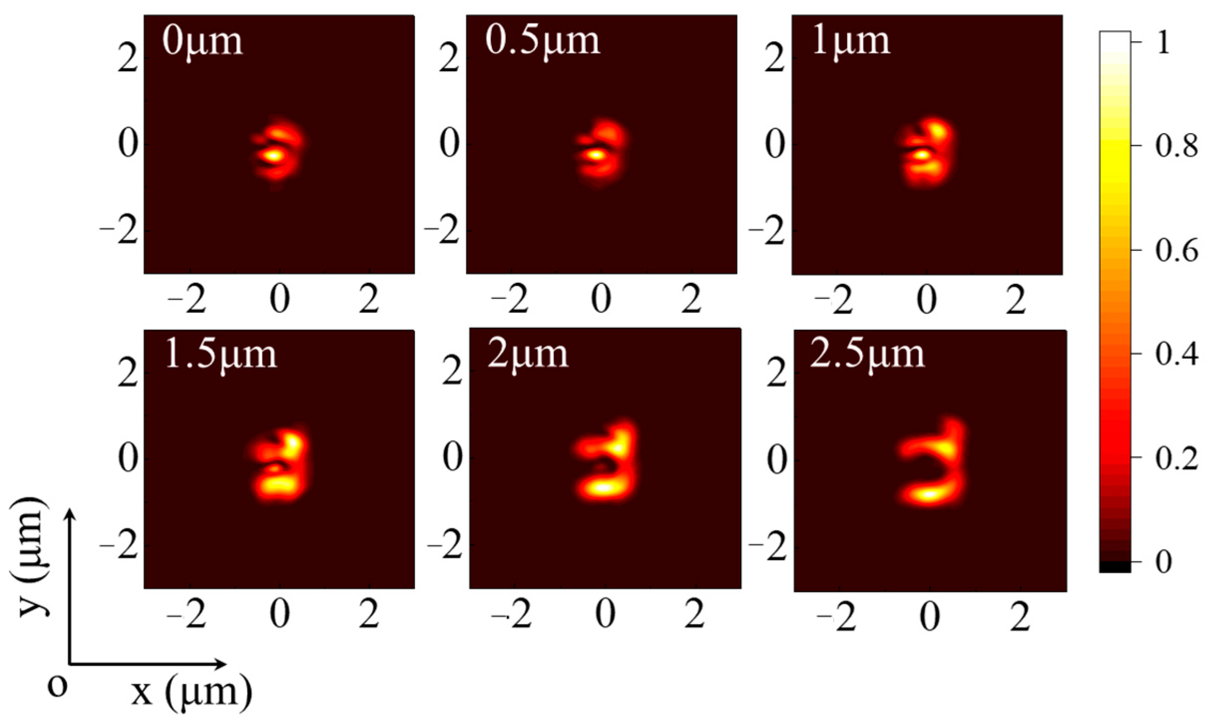
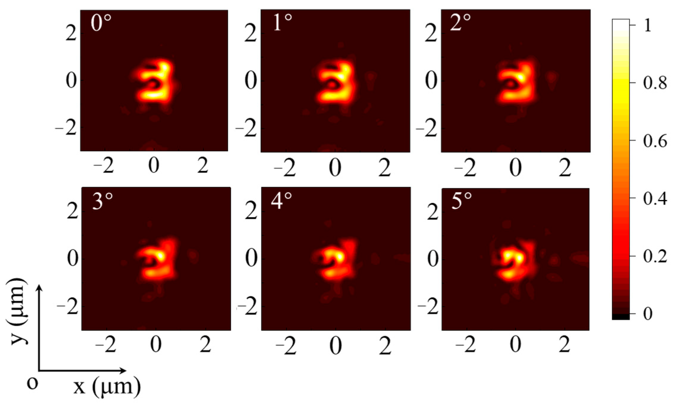
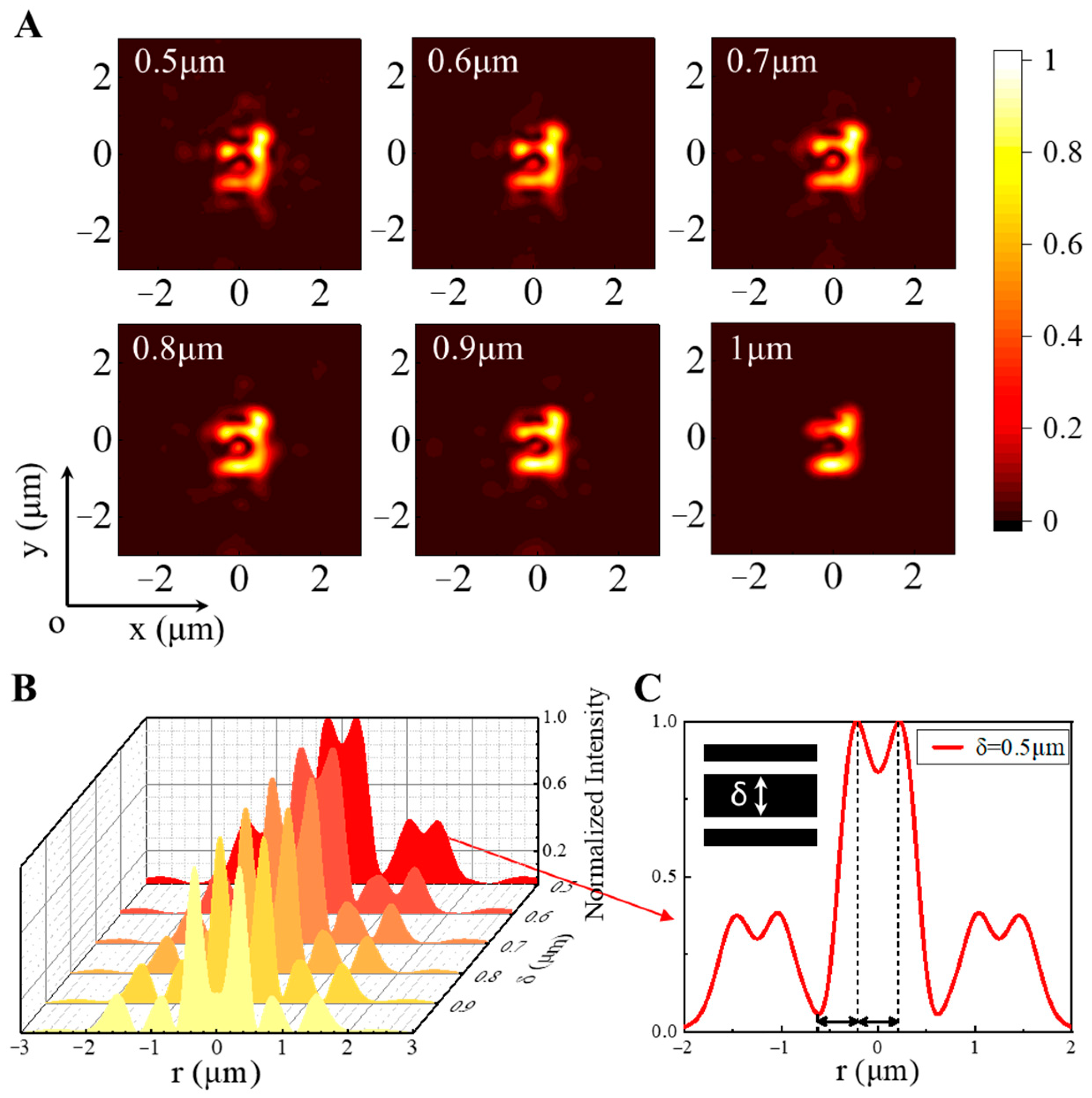
In recent years, the design of doublet metalenses [6,61,62] has also been proposed. To reduce the simulation data, in this paper, we choose the diameters of the two metalenses as R1 = 3 μm, R2 = 0.75 μm, and the focal lengths as f1 = 6 μm and f2 = 1.5 μm. Among them, Figure 5A is the intensity map of the xz plane. The shaded part of the box is the position of the two metalenses. The dashed line indicates the focal plane position of metalens L1, located at a distance of 6 μm from metalens L1. It is precisely focused on the focal position of metalens L2 to obtain the outgoing parallel light. Figure 5B shows the phase distribution on the xz plane. A simulation material with total reflection properties is added to the periphery of the two metalenses as a diaphragm to limit stray light. The reflected light is messy and affects the substrate’s phase distribution. However, according to Figure 5B, we can observe that after passing through metalens L2, the phase distribution of the outgoing light is flat. Amplifying and analyzing the phase distribution in the purple box in Figure 5B, the phase of the outgoing light is very flat and close to the phase of parallel light.
Based on the above analysis, we quantitatively analyze the flatness of the emitted light. We select the phase of the outgoing light propagation distance dz of 1, 1.5, 2, 2.5, 3, 3.5, 4 μm, and dz is the distance after metalens L2. We define the difference between the actual and ideal phases at different propagation distances after the integrated doublet metalens as the wave phase difference (WPD). As shown in Figure 6A, the phase fluctuates slightly when the propagation distance is relatively short. Nevertheless, after the propagation distance reaches 2 μm, the propagation phase tends to be flat, and the maximum fluctuation is controlled within 0.03 times 2π (the phase of one wavelength). The average value (AV), variance, and standard deviation of the phase difference curve at different propagation distances are analyzed in Figure 6B. The standard deviation and variance can reflect the degree of dispersion of each phase difference curve dataset. When the propagation distance dz is greater than 2 μm, the flatness of the emitted light is better, and the average value is controlled within 0.022 times 2π.
Table 1 lists the AV of the wave phase difference and the peak-valley (PV) value under different propagation distances. The PV value is the difference between the maximum and minimum values in the phase difference curve data. When the propagation distance reaches 2 μm, we obtain the wave phase difference with the minimum average value, and its variance and standard deviation are also considered the smallest.
At the same time, we analyze the efficiency of the integrated doublet metalens. The transmittance of the integrated deep ultraviolet doublet metalens is 46.21%. The output area is 1/16 of the incident area, so the light intensity per unit area of the emitted light is 7.39 times the intensity of the incident light per unit area.

3. Results

To further verify the possibility of applying the design to deep ultraviolet lithography, we set up a “mask” in the simulation. We added light-shielding materials in front of metalens L1 (in front of the overall structure) to observe the imaging conditions. For better verification, we chose the “F” pattern, as shown in Figure 7. The “F” pattern has asymmetry, which can be used to analyze the imaging capability of the doublet metalens system more clearly. Due to the limitations in computer simulation capabilities, the overall size of the doublet metalens that we designed was small, so the diffraction effect was unavoidable. To reduce the influence of diffraction as much as possible, we set its position close to the front side of metalens L1.
As shown in Figure 7A, we set a = b = 1 μm of the “F” pattern for simulation. Figure 8 displays the various intensity patterns at different distances behind metalens L2: 1.5, 2, 2.5, and 3 μm. According to the simulation results, we can observe a more explicit “F” pattern in the inverted upside-down images.
However, simultaneously, the imaging also tends to increase as the distance increases. This phenomenon does not conform to the imaging law of the afocal system that we designed. We believe that it is due to the small overall size of the doublet metalens, which has the diffraction effect. Analyzing the propagation distance, we suggest that the diffraction type is Fresnel diffraction. To verify our judgment, we perform an inverse diffraction calculation. Using the intensity simulation results at 3 μm as the original image, we calculate the intensity pattern before 3 μm at different locations only affected by diffraction. The transfer function of Fresnel diffraction is
H = exp i k z exp i π λ z f x 2 + f y 2
Among them, k = /λ is the wavenumber, z represents the distance between the observation screen and the diffraction screen, and fx and fy are the spatial frequencies of the complex amplitude distribution in the x and y directions. Then, the transfer function of Fresnel inverse diffraction is
H 1 = exp i k z exp i π λ z f x 2 + f y 2
By applying the abovementioned formula, we can calculate the complex amplitude using the intensity and phase data at a distance of 3 μm from L2. This can be used to perform inverse diffraction, which allows us to obtain the intensity distribution at different distances from the source plane. The resulting distribution is illustrated in Figure 9. We compare the actual simulation results at different positions in Figure 8 with the results obtained by the inverse diffraction calculation in Figure 9. It can be seen that the outer frame size of the pattern is the same for the same propagation distance. This indicates that the gradual increase in the pattern with increasing propagation distance is due to the diffraction effect. The diffraction effect will be significantly reduced when the size of the two metalenses is large enough compared with the working wavelength.
However, the consideration of how to further reduce the influence of diffraction by optimizing the design is essential for our next step. Meanwhile, based on the pattern calculated by the inverse diffraction method at 0 μm, we can find that the overall pattern size has reached the expected ratio of 4:1. However, according to the analysis of Figure 5 and Figure 6, it can be seen that the phase of the near field is uneven to an extent. As a result, the pattern after the inverse diffraction calculation is also somewhat unclear. However, we have obtained a relatively straightforward and complete imaging pattern at a propagation distance of 2 μm, with the imaging pattern being one half of the size of the original mask pattern. Therefore, we can adjust the size and focal length of the two metalenses according to the required imaging ratio to obtain a pattern corresponding to the ratio of the propagation distance of the precise pattern.
At the same time, the system proposed in this paper has relatively high tolerance to the incident angle. When the angle of incidence is changed, the intensity distribution at the propagation distance of 2 μm is as shown in Figure 10. From the phase analysis in Figure 6, it can be seen that the phase is the flattest when the propagation distance is 2 μm, and the imaging results are also comparatively analyzed. At oblique incidence, the incidence angle varies from 0° to 5°, and the step is 1°. It can be observed that when the incident light angle is deflected to 3°, there is still a distinguishable projection imaging effect.
We analyzed the resolving power of the doublet metalens, as shown in Figure 11. The overall dimensions Dx and Dy of the “F” pattern are determined to be 3 μm and 4 μm, respectively. The intensity distribution at a distance of 2 μm is shown in Figure 11A, with the width a of the transmission stripe decreasing continuously. When the width of the light-transmitting fringe is reduced to 0.5 μm, a distinguishable intensity image can still be obtained.
To further analyze the resolving power of the doublet metalens, the transmitted edge is fixed at 0.5 μm, and the distance δ between the two edges is varied. Figure 11B,C show the intensity distribution at a propagation distance of 2 μm. When δ is 1 μm, two bright stripes with clear boundaries can be observed. As δ gradually decreases, the two bright stripes slowly approach each other. Refer to Rayleigh’s criterion: when the edge of one Airy spot coincides with the center of another, the corresponding two object points can be distinguished. Therefore, when δ = 0.5 μm, two bright stripes can be distinguished.

4. Conclusions

A series of problems are observed in the existing deep ultraviolet optical system, such as complex and large systems, limited ray incidence angles, and complex system aberration. The metalens provides a new design idea for optical systems because of its powerful wavefront control ability. Based on the transmission metalens, an integrated deep ultraviolet all-dielectric doublet metalens that can reduce beams and realize projection imaging is proposed. Based on the design idea of the Huygens electromagnetic metasurface, a series of high-transmittance and controllable dielectric artificial atoms covering the 2π transmission phase are combined to realize the metalens. On this basis, an integrated ultra-violet all-dielectric doublet metalens is designed to convert the large beams of a large deep ultraviolet facility into beams with a smaller diameter. We find that the light intensity per unit area of the emitted light is 7.39 times that of the incident light unit area. At the same time, the projection imaging of the mask is simulated, which proves that the doublet metalens can achieve clear and discernible projection imaging. Its resolution and angle tolerance are analyzed, showing good results. We can adjust the size and focal length of the two metalenses according to the required imaging ratio to obtain a pattern corresponding to the ratio of the propagation distance of the clear pattern. The doublet metalens is suitable for the objective lens systems of deep ultraviolet lithography machines, with the advantages of being ultra-light, ultra-thin, and easy to integrate. The doublet metalens also has the advantages of a simple structure, stability, and low installation precision. At the same time, the doublet metalens can also be used as an expanding mirror, and it has some application prospects in laser beam combination and deep ultraviolet space camera lighting systems, opening up new opportunities for micro-nano optical imaging and optoelectronic equipment. The optical system can also be used as a beam expander. It can effectively reduce the number of lenses in the ultraviolet system, with high transmittance and low energy loss. It opens up a new path for ultraviolet optical imaging and optoelectronic equipment.

Author Contributions

Conceptualization, X.S. and Z.L.; methodology, X.S. and F.Y.; software, X.S. and E.H.; validation, X.S., F.Y. and E.H.; formal analysis, X.S.; investigation, X.S.; resources, X.S.; data curation, X.S.; writing—original draft preparation, X.S.; writing—review and editing, X.S.; visualization, X.S.; supervision, Z.L.; project administration, Z.L.; funding acquisition, Z.L. All authors have read and agreed to the published version of the manuscript.

Funding

Distinguished Young Scholars of Jilin Province (20230101351JC); Scientific and Technological Development Project of Jilin Province (20220201080GX); National Natural Science Foundation of China (61735018); Excellent Member of Youth Innovation Promotion Association of the Chinese Academy of Sciences (Y201836); Leading Talents and Team Project of Scientific and Technological Innovation for Young and Middle-Aged Groups in Jilin Province (20190101012JH).

Institutional Review Board Statement

Not applicable.

Informed Consent Statement

Not applicable.

Data Availability Statement

Data are contained within the article.

Acknowledgments

The authors thank Enzhu Hou of the Northeast Normal University for the technical assistance in the figure drawing and literature investigation.

Conflicts of Interest

The authors declare no conflicts of interest.

References

  1. Chang, C.C.; Kort-Kamp, W.J.M.; Nogan, J.; Luk, T.S.; Azad, A.K.; Taylor, A.J.; Dalvit, D.A.R.; Sykora, M.; Chen, H.T. High-Temperature Refractory Metasurfaces for Solar Thermophotovoltaic Energy Harvesting. Nano Lett. 2018, 18, 7665–7673. [Google Scholar] [CrossRef]
  2. Decker, M.; Chen, W.T.; Nobis, T.; Zhu, A.Y.; Khorasaninejad, M.; Bharwani, Z.; Capasso, F.; Petschulat, J. Imaging Performance of Polarization-Insensitive Metalenses. ACS Photonics 2019, 6, 1493–1499. [Google Scholar] [CrossRef]
  3. Mohtashami, Y.; DeCrescent, R.A.; Heki, L.K.; Iyer, P.P.; Butakov, N.A.; Wong, M.S.; Alhassan, A.; Mitchell, W.J.; Nakamura, S.; DenBaars, S.P.; et al. Light-emitting metalenses and meta-axicons for focusing and beaming of spontaneous emission. Nat. Commun. 2021, 12, 3591. [Google Scholar] [CrossRef] [PubMed]
  4. Guo, Y.; Pu, M.; Ma, X.; Li, X.; Shi, R.; Luo, X. Experimental demonstration of a continuous varifocal metalens with large zoom range and high imaging resolution. Appl. Phys. Lett. 2019, 115, 163103. [Google Scholar] [CrossRef]
  5. Luo, Y.; Chu, C.H.; Vyas, S.; Kuo, H.Y.; Chia, Y.H.; Chen, M.K.; Shi, X.; Tanaka, T.; Misawa, H.; Huang, Y.Y.; et al. Varifocal Metalens for Optical Sectioning Fluorescence Microscopy. Nano Lett. 2021, 21, 5133–5142. [Google Scholar] [CrossRef] [PubMed]
  6. Wei, Y.; Wang, Y.; Feng, X.; Xiao, S.; Wang, Z.; Hu, T.; Hu, M.; Song, J.; Wegener, M.; Zhao, M.; et al. Compact Optical Polarization-Insensitive Zoom Metalens Doublet. Adv. Opt. Mater. 2020, 8, 2000142. [Google Scholar] [CrossRef]
  7. Hua, J.; Hua, E.; Zhou, F.; Shi, J.; Wang, C.; Duan, H.; Hu, Y.; Qiao, W.; Chen, L. Foveated glasses-free 3D display with ultrawide field of view via a large-scale 2D-metagrating complex. Light-Sci. Appl. 2021, 10, 213. [Google Scholar] [CrossRef] [PubMed]
  8. Spagele, C.; Tamagnone, M.; Kazakov, D.; Ossiander, M.; Piccardo, M.; Capasso, F. Multifunctional wide-angle optics and lasing based on supercell metasurfaces. Nat. Commun. 2021, 12, 3787. [Google Scholar] [CrossRef]
  9. Wang, L.; Kruk, S.; Tang, H.; Li, T.; Kravchenko, I.; Neshev, D.N.; Kivshar, Y.S. Grayscale transparent metasurface holograms. Optica 2016, 3, 194. [Google Scholar] [CrossRef]
  10. Dixon, K.; Montazeri, A.O.; Shayegannia, M.; Barnard, E.S.; Cabrini, S.; Matsuura, N.; Holman, H.Y.; Kherani, N.P. Tunable rainbow light trapping in ultrathin resonator arrays. Light-Sci. Appl. 2020, 9, 194. [Google Scholar] [CrossRef]
  11. Holsteen Aaron, L.; Cihan Ahmet, F.; Brongersma Mark, L. Temporal color mixing and dynamic beam shaping with silicon metasurfaces. Science 2019, 365, 257–260. [Google Scholar] [CrossRef]
  12. Zhang, X.; Li, Q.; Liu, F.; Qiu, M.; Sun, S.; He, Q.; Zhou, L. Controlling angular dispersions in optical metasurfaces. Light-Sci. Appl. 2020, 9, 76. [Google Scholar] [CrossRef] [PubMed]
  13. Grant, J.; Kenney, M.; Shah, Y.D.; Escorcia-Carranza, I.; Cumming, D.R.S. CMOS compatible metamaterial absorbers for hyperspectral medium wave infrared imaging and sensing applications. Opt. Express 2018, 26, 10408–10420. [Google Scholar] [CrossRef] [PubMed]
  14. Lochbaum, A.; Fedoryshyn, Y.; Dorodnyy, A.; Koch, U.; Hafner, C.; Leuthold, J. On-Chip Narrowband Thermal Emitter for Mid-IR Optical Gas Sensing. ACS Photonics 2017, 4, 1371–1380. [Google Scholar] [CrossRef]
  15. Chen, S.; Xie, Z.; Ye, H.; Wang, X.; Guo, Z.; He, Y.; Li, Y.; Yuan, X.; Fan, D. Cylindrical vector beam multiplexer/demultiplexer using off-axis polarization control. Light-Sci. Appl. 2021, 10, 222. [Google Scholar] [CrossRef]
  16. Dorrah, A.H.; Rubin, N.A.; Tamagnone, M.; Zaidi, A.; Capasso, F. Structuring total angular momentum of light along the propagation direction with polarization-controlled meta-optics. Nat. Commun. 2021, 12, 6249. [Google Scholar] [CrossRef] [PubMed]
  17. Dorrah, A.H.; Rubin, N.A.; Zaidi, A.; Tamagnone, M.; Capasso, F. Metasurface optics for on-demand polarization transformations along the optical path. Nat. Photonics 2021, 15, 287–296. [Google Scholar] [CrossRef]
  18. Aydin, K.; Ferry, V.E.; Briggs, R.M.; Atwater, H.A. Broadband polarization-independent resonant light absorption using ultrathin plasmonic super absorbers. Nat. Commun. 2011, 2, 517. [Google Scholar] [CrossRef]
  19. Contractor, R.; D’Aguanno, G.; Menyuk, C. Ultra-broadband, polarization-independent, wide-angle absorption in impedance-matched metamaterials with anti-reflective moth-eye surfaces. Opt. Express 2018, 26, 24031–24043. [Google Scholar] [CrossRef]
  20. Du, C.; Zhou, D.; Guo, H.H.; Pang, Y.Q.; Shi, H.Y.; Liu, W.F.; Su, J.Z.; Singh, C.; Trukhanov, S.; Trukhanov, A.; et al. An ultra-broadband terahertz metamaterial coherent absorber using multilayer electric ring resonator structures based on anti-reflection coating. Nanoscale 2020, 12, 9769–9775. [Google Scholar] [CrossRef]
  21. Fan, K.; Suen, J.Y.; Liu, X.; Padilla, W.J. All-dielectric metasurface absorbers for uncooled terahertz imaging. Optica 2017, 4, 601–604. [Google Scholar] [CrossRef]
  22. Hoa, N.T.Q.; Lam, P.H.; Tung, P.D.; Tuan, T.S.; Nguyen, H. Numerical Study of a Wide-Angle and Polarization-Insensitive Ultrabroadband Metamaterial Absorber in Visible and Near-Infrared Region. IEEE Photonics J. 2019, 11, 4600208. [Google Scholar] [CrossRef]
  23. Yesilkoy, F.; Arvelo, E.R.; Jahani, Y.; Liu, M.; Tittl, A.; Cevher, V.; Kivshar, Y.; Altug, H. Ultrasensitive hyperspectral imaging and biodetection enabled by dielectric metasurfaces. Nat. Photonics 2019, 13, 390–396. [Google Scholar] [CrossRef]
  24. Dolia, V.; Balch, H.; Dagli, S.; Abdollahramezani, S.; Delgado, H.; Moradifar, P.; Chang, K.; Stiber, A.; Safir, F.; Lawrence, M.; et al. Very-Large-Scale Integrated High-Q Nanoantenna Pixels (VINPix). arXiv 2023, arXiv:2310.08065. [Google Scholar]
  25. Zhao, M.; Chen, M.K.; Zhuang, Z.P.; Zhang, Y.; Chen, A.; Chen, Q.; Liu, W.; Wang, J.; Chen, Z.M.; Wang, B.; et al. Phase characterisation of metalenses. Light-Sci. Appl. 2021, 10, 52. [Google Scholar] [CrossRef] [PubMed]
  26. Gao, S.; Park, C.S.; Zhou, C.; Lee, S.S.; Choi, D.Y. Twofold Polarization-Selective All-Dielectric Trifoci Metalens for Linearly Polarized Visible Light. Adv. Opt. Mater. 2019, 7, 1900883. [Google Scholar] [CrossRef]
  27. Engelberg, J.; Zhou, C.; Mazurski, N.; Bar-David, J.; Kristensen, A.; Levy, U. Near-IR wide-field-of-view Huygens metalens for outdoor imaging applications. Nanophotonics 2020, 9, 361–370. [Google Scholar] [CrossRef]
  28. Liang, H.; Lin, Q.; Xie, X.; Sun, Q.; Wang, Y.; Zhou, L.; Liu, L.; Yu, X.; Zhou, J.; Krauss, T.F.; et al. Ultrahigh Numerical Aperture Metalens at Visible Wavelengths. Nano Lett. 2018, 18, 4460–4466. [Google Scholar] [CrossRef] [PubMed]
  29. Paniagua-Dominguez, R.; Yu, Y.F.; Khaidarov, E.; Choi, S.; Leong, V.; Bakker, R.M.; Liang, X.; Fu, Y.H.; Valuckas, V.; Krivitsky, L.A.; et al. A Metalens with a Near-Unity Numerical Aperture. Nano Lett. 2018, 18, 2124–2132. [Google Scholar] [CrossRef]
  30. Hu, M.; Wei, Y.; Cai, H.; Cai, Y. Polarization-insensitive and achromatic metalens at ultraviolet wavelengths. J. Nanophotonics 2019, 13, 036015. [Google Scholar] [CrossRef]
  31. Balli, F.; Sultan, M.A.; Ozdemir, A.; Hastings, J.T. An ultrabroadband 3D achromatic metalens. Nanophotonics 2021, 10, 1259–1264. [Google Scholar] [CrossRef]
  32. Chen, W.T.; Zhu, A.Y.; Sisler, J.; Bharwani, Z.; Capasso, F. A broadband achromatic polarization-insensitive metalens consisting of anisotropic nanostructures. Nat. Commun. 2019, 10, 355. [Google Scholar] [CrossRef] [PubMed]
  33. Cheng, K.; Wei, Z.; Fan, Y.; Zhang, X.; Wu, C.; Li, H. Realizing Broadband Transparency via Manipulating the Hybrid Coupling Modes in Metasurfaces for High-Efficiency Metalens. Adv. Opt. Mater. 2019, 7, 1900016. [Google Scholar] [CrossRef]
  34. Deng, Y.; Wang, X.; Gong, Z.; Dong, K.; Lou, S.; Pegard, N.; Tom, K.B.; Yang, F.; You, Z.; Waller, L.; et al. All-Silicon Broadband Ultraviolet Metasurfaces. Adv. Mater. 2018, 30, e1802632. [Google Scholar] [CrossRef] [PubMed]
  35. Hu, T.; Feng, X.; Yang, Z.; Zhao, M. Design of scalable metalens array for optical addressing. Front. Optoelectron. 2022, 15, 32. [Google Scholar] [CrossRef] [PubMed]
  36. Ossiander, M.; Meretska, M.L.; Hampel, H.K.; Lim, S.W.D.; Knefz, N.; Jauk, T.; Capasso, F.; Schultze, M. Extreme ultraviolet metalens by vacuum guiding. Science 2023, 380, 59–63. [Google Scholar] [CrossRef] [PubMed]
  37. Hemmatyar, O.; Abdollahramezani, S.; Kiarashinejad, Y.; Zandehshahvar, M.; Adibi, A. Full color generation with Fano-type resonant HfO2 nanopillars designed by a deep-learning approach. Nanoscale 2019, 11, 21266–21274. [Google Scholar] [CrossRef] [PubMed]
  38. Kim, J.; Kim, W.; Oh, D.K.; Kang, H.; Kim, H.; Badloe, T.; Kim, S.; Park, C.; Choi, H.; Lee, H.; et al. One-step printable platform for high-efficiency metasurfaces down to the deep-ultraviolet region. Light Sci. Appl. 2023, 12, 68. [Google Scholar] [CrossRef]
  39. Zhou, Y.; Kravchenko, I.I.; Wang, H.; Zheng, H.; Gu, G.; Valentine, J. Multifunctional metaoptics based on bilayer metasurfaces. Light Sci. Appl. 2019, 8, 80. [Google Scholar] [CrossRef]
  40. Mansouree, M.; Kwon, H.; Arbabi, E.; McClung, A.; Faraon, A.; Arbabi, A.J.O. Multifunctional 25D metastructures enabled by adjoint optimization. Optica 2020, 7, 77–84. [Google Scholar] [CrossRef]
  41. Baksh Peter, D.; Ostrčil, M.; Miszczak, M.; Pooley, C.; Chapman Richard, T.; Wyatt Adam, S.; Springate, E.; Chad John, E.; Deinhardt, K.; Frey Jeremy, G.; et al. Quantitative and correlative extreme ultraviolet coherent imaging of mouse hippocampal neurons at high resolution. Sci. Adv. 2020, 6, eaaz3025. [Google Scholar] [CrossRef] [PubMed]
  42. Riedel, R.; Al-Shemmary, A.; Gensch, M.; Golz, T.; Harmand, M.; Medvedev, N.; Prandolini, M.J.; Sokolowski-Tinten, K.; Toleikis, S.; Wegner, U.; et al. Single-shot pulse duration monitor for extreme ultraviolet and X-ray free-electron lasers. Nat. Commun. 2013, 4, 1731. [Google Scholar] [CrossRef] [PubMed]
  43. Zheng, X.; Jia, Y.; Chen, A. Azobenzene-containing liquid crystalline composites for robust ultraviolet detectors based on conversion of illuminance-mechanical stress-electric signals. Nat. Commun. 2021, 12, 4875. [Google Scholar] [CrossRef] [PubMed]
  44. Cai, Q.; You, H.; Guo, H.; Wang, J.; Liu, B.; Xie, Z.; Chen, D.; Lu, H.; Zheng, Y.; Zhang, R. Progress on AlGaN-based solar-blind ultraviolet photodetectors and focal plane arrays. Light-Sci. Appl. 2021, 10, 94. [Google Scholar] [CrossRef] [PubMed]
  45. Xu, T.; Agrawal, A.; Abashin, M.; Chau, K.J.; Lezec, H.J. All-angle negative refraction and active flat lensing of ultraviolet light. Nature 2013, 497, 470–474. [Google Scholar] [CrossRef] [PubMed]
  46. Kuai, Y.; Chen, J.; Tang, X.; Xiang, Y.; Lu, F.; Kuang, C.; Xu, L.; Shen, W.; Cheng, J.; Gui, H.; et al. Label-free surface-sensitive photonic microscopy with high spatial resolution using azimuthal rotation illumination. Sci. Adv. 2019, 5, eaav5335. [Google Scholar] [CrossRef] [PubMed]
  47. Shi, J.; Wong, T.T.W.; He, Y.; Li, L.; Zhang, R.; Yung, C.S.; Hwang, J.; Maslov, K.; Wang, L.V. High-resolution, high-contrast mid-infrared imaging of fresh biological samples with ultraviolet-localized photoacoustic microscopy. Nat. Photonics 2019, 13, 609–615. [Google Scholar] [CrossRef]
  48. Zhao, Y.; Sun, F.; Tong, C.; Shu, S.; Hou, G.; Lu, H.; Zhang, X.; Wang, L.; Tian, S.; Wang, L. Going beyond the beam quality limit of spectral beam combining of diode lasers in a V-shaped external cavity. Opt. Express 2018, 26, 14058–14065. [Google Scholar] [CrossRef]
  49. Sun, F.; Shu, S.; Zhao, Y.; Hou, G.; Lu, H.; Zhang, X.; Wang, L.; Tian, S.; Tong, C.; Wang, L. High-brightness diode lasers obtained via off-axis spectral beam combining with selective feedback. Opt. Express 2018, 26, 21813–21818. [Google Scholar] [CrossRef]
  50. Nikolov, D.K.; Bauer, A.; Cheng, F.; Kato, H.; Vamivakas, A.N.; Rolland, J.P. Metaform optics: Bridging nanophotonics and freeform optics. Sci. Adv. 2021, 7, eabe5112. [Google Scholar] [CrossRef]
  51. Palik, E.D. Handbook of Optical Constants of Solids; Academic Press: Cambridge, MA, USA, 1985. [Google Scholar]
  52. Lin, R.J.; Su, V.C.; Wang, S.; Chen, M.K.; Chung, T.L.; Chen, Y.H.; Kuo, H.Y.; Chen, J.W.; Chen, J.; Huang, Y.T.; et al. Achromatic metalens array for full-colour light-field imaging. Nat. Nanotechnol. 2019, 14, 227–231. [Google Scholar] [CrossRef] [PubMed]
  53. Li, S.; Zhou, C.; Ban, G.; Wang, H.; Lu, H.; Wang, Y. Active all-dielectric bifocal metalens assisted by germanium antimony telluride. J. Phys. D Appl. Phys. 2019, 52, 095106. [Google Scholar] [CrossRef]
  54. Chantakit, T.; Schlickriede, C.; Sain, B.; Meyer, F.; Weiss, T.; Chattham, N.; Zentgraf, T. All-dielectric silicon metalens for two-dimensional particle manipulation in optical tweezers. Photon. Res. 2020, 8, 1435–1440. [Google Scholar] [CrossRef]
  55. Pu, M.; Ma, X.; Wang, C.; Luo, X.; Li, X.; Hong, M.; Wang, M.; Wu, X. Characteristics of a mid-wavelength infrared metalenses integrated imaging system. In Proceedings of the 9th International Symposium on Advanced Optical Manufacturing and Testing Technologies: Meta-Surface-Wave and Planar Optics, Chengdu, China, 26–29 June 2018. [Google Scholar]
  56. Guo, L.; Hu, Z.; Wan, R.; Long, L.; Li, T.; Yan, J.; Lin, Y.; Zhang, L.; Zhu, W.; Wang, L. Design of aluminum nitride metalens for broadband ultraviolet incidence routing. Nanophotonics 2018, 8, 171–180. [Google Scholar] [CrossRef]
  57. Guo, H.; Yue, S.; Wang, R.; Hou, Y.; Li, M.; Zhang, K.; Zhang, Z. Design of Polarization-Independent Reflective Metalens in the Ultraviolet-Visible Wavelength Region. Nanomaterials 2021, 11, 1243. [Google Scholar] [CrossRef] [PubMed]
  58. Kanwal, S.; Wen, J.; Yu, B.; Kumar, D.; Chen, X.; Kang, Y.; Bai, C.; Zhang, D. High-Efficiency, Broadband, Near Diffraction-Limited, Dielectric Metalens in Ultraviolet Spectrum. Nanomaterials 2020, 10, 490. [Google Scholar] [CrossRef] [PubMed]
  59. Ali, F.; Aksu, S. A hybrid broadband metalens operating at ultraviolet frequencies. Sci. Rep. 2021, 11, 2303. [Google Scholar] [CrossRef]
  60. Chen, C.; Song, W.; Chen, J.W.; Wang, J.H.; Chen, Y.H.; Xu, B.; Chen, M.K.; Li, H.; Fang, B.; Chen, J.; et al. Spectral tomographic imaging with aplanatic metalens. Light-Sci. Appl. 2019, 8, 99. [Google Scholar] [CrossRef]
  61. Kim, C.; Kim, S.J.; Lee, B. Doublet metalens design for high numerical aperture and simultaneous correction of chromatic and monochromatic aberrations. Opt. Express 2020, 28, 18059–18076. [Google Scholar] [CrossRef]
  62. Groever, B.; Chen, W.T.; Capasso, F. Meta-Lens Doublet in the Visible Region. Nano Lett. 2017, 17, 4902–4907. [Google Scholar] [CrossRef]
Figure 1. (A) A schematic illustration of a deep ultraviolet integrated doublet metalens. (B) Side view of deep ultraviolet integrated doublet metalens. (C) Side view, top view, and three-dimensional view of the unit structure, respectively. The height of the cylinder is h, the radius is r, and the unit structure period is D. (D) The relationship between the phase control of the unit structure and the radius.
Applsci 14 01316 g001
Figure 2. (A) The change in the phase delay with the evolution of the cylinder radius r and height h. (B) The transmittance changes with the cylinder radius r and height h change. (C) The full-wave simulations (E, H, and P) of meta-units with different radii (30, 40, 50, and 60 nm).
Applsci 14 01316 g002
Figure 3. (A) Metalens focusing diagram. (B) Metalens L1 is a standard and aspherical phase profile. (C) Metalens L2 is a normal and aspherical phase profile.
Applsci 14 01316 g003
Figure 4. (AC) The focusing effects of metalens L1: the normalized energy map of the xz plane; the normalized energy map of the focal plane (xy plane); the radial normalized energy distribution. (DF) The focusing effects of metalens L2: the normalized energy map of the xz plane; the normalized energy map of the xy plane of the focal plane; and the normalized energy distribution of the radial direction.
Applsci 14 01316 g004
Figure 5. The simulation results of the integrated doublet metalens. (A) The energy distribution when the incident light is parallel (xz plane). (B) The phase distribution when the incident light is parallel (xz plane). The right figure shows the outgoing light’s phase distribution after the integrated doublet metalens (xz plane).
Applsci 14 01316 g005
Figure 6. Analysis of the parallelism of the emitted light. (A) The WPD at different propagation distances after the integrated doublet metalens. (B) The average, standard deviation, and variance of the WPD at different propagation distances after the integrated doublet metalens.
Applsci 14 01316 g006
Figure 7. (A) The reticle pattern added to the simulation. (B) The reticle’s position in the doublet metalens’s optical system.
Applsci 14 01316 g007
Figure 8. Image intensity map at different propagation distances behind the doublet metalens.
Applsci 14 01316 g008
Figure 9. The inverse diffraction calculation with a propagation distance of 0, 0.5, 1, 1.5, 2, 2.5 μm is performed on the simulated intensity map with a propagation distance of 3 μm.
Applsci 14 01316 g009
Figure 10. The intensity distribution diagram is obtained at 2 μm when the incident light is deflected at different angles.
Applsci 14 01316 g010
Figure 11. Resolution analysis of doublet metalens. (A) The setting of the bright and dark stripes, where the interval between the two bright stripes is δ, is the intensity obtained when δ is 0.5 μm. (B) Intensity diagrams at a propagation distance of 2 μm when the light-transmitting fringe width a is 0.5, 0.6, 0.7, 0.8, 0.9, and 1 μm, respectively. (C) Change in the value of the interval δ between the two bright stripes to obtain the intensity.
Applsci 14 01316 g011
Table 1. Average value and peak-valley value of wave difference after different propagation distances.
dx (μm)11.522.533.54
AV (2π)0.085880.08720.009950.014260.018180.019910.02225
PV (2π)0.153110.166160.022680.021450.024110.024650.03073
Disclaimer/Publisher’s Note: The statements, opinions and data contained in all publications are solely those of the individual author(s) and contributor(s) and not of MDPI and/or the editor(s). MDPI and/or the editor(s) disclaim responsibility for any injury to people or property resulting from any ideas, methods, instructions or products referred to in the content.

