Article

Analysis, Design, and Experimental Validation of a High-Isolation, Low-Cross-Polarization Antenna Array Demonstrator for Software-Defined-Radar Applications

by
Nicholas Ricciardella
1,†,
Walter Fuscaldo
2,*,†,
Tito Mattei
1,†,
Anna Maria Fiorello
1,†,
Leopoldo Infante
1,† and
Alessandro Galli
3,†
1
Electronics Division Leonardo SpA, 00131 Rome, Italy
2
Consiglio Nazionale delle Ricerche, Istituto per la Microelettronica e Microsistemi, 00133 Rome, Italy
3
Department of Information Engineering, Electronics and Telecommunications, Sapienza University of Rome, 00184 Rome, Italy
*
Author to whom correspondence should be addressed.
These authors contributed equally to this work.
Appl. Sci. 2024, 14(14), 6015; https://doi.org/10.3390/app14146015
Submission received: 23 May 2024 / Revised: 17 June 2024 / Accepted: 27 June 2024 / Published: 10 July 2024

Abstract

:
In a software-defined radar (SDR) system, most of the signal processing usually implemented in hardware is implemented by software, thus allowing for higher flexibility and modularity compared to conventional radar systems. However, the majority of SDR demonstrators and proofs of concept reported in the open literature so far have been based on simple antenna systems. As a result, the full potentialities of an SDR approach have not been completely exploited yet. In this work, we propose a flexible antenna module to be integrated into an active electronically scanning array (AESA) with controlled sidelobe level over a wide angular range, exhibiting polarization reconfigurability with a low cross-polarization level and high isolation. For this purpose, analytical and numerically efficient techniques for the synthesis of the aperture distribution and the correct evaluation of the radiating features (e.g., beamwidth, pointing angle, sidelobe levels, etc.) are presented in order to grant real-time control of the digital beamforming network. A sub-array module demonstrator is fabricated and measured to corroborate the concept.

1. Introduction

In the last few years, the attention on software-defined radar (SDR) has grown exponentially. As a matter of fact, this approach offers a series of advantages that goes from digital beamforming to hardware flexibility [1]. The possibility to drive an active electronically scanning array (AESA) with an SDR platform [2,3,4,5] would pave the way for a fully digital radio-frequency (RF) front-end with unprecedented capabilities in terms of reconfigurability, re-use of hardware, and modularity.
Recently, SDR platforms have been configured and tested to drive passive bistatic radar (PBR) systems based on linear arrays to perform detection and tracking functions. These works [6,7,8,9] were mainly focused on the software implementation of the calibration network and of the digital signal processing (DSP) architecture. However, in order to fully exploit the potentialities of the SDR approach, design flexibility has to be ensured at the hardware level. Antenna elements that allow for dynamic polarization and beam steering are thus required, especially when used in large planar AESA, to reach the high gain and high coverage requirements of radar tracking systems.
In order to respond to the needs of design flexibility and high performance, inspired by the recent works on multifunction phased array radar (MPAR) [10,11,12], we propose here an attractive unit cell fed with two ports that can be independently controlled in amplitude and phase, and that is capable of providing low cross-polarization and high isolation levels without using additional techniques, such as decoupling networks. In order to corroborate the antenna performance, a 4 × 8 array demonstrator is fabricated whereas the gain and reflection coefficient of a 4 × 6 array are measured, showing good agreement with the expected theoretical results for the single radiating element in a periodic environment.
This preliminary demonstration paves the way for targeting the development of larger AESA panels, thanks to the modularity of the proposed sub-array architecture. Specifically, we will also discuss here the system requirements of a 40 × 40 planar AESA capable of scanning a very directive beam over a wide angular range with controlled sidelobes in C band. Efficient analytical and numerical methods for the realization of a Tseng–Cheng beamforming network [13] and the evaluation of the main radiating properties are proposed to easily interface the AESA with an SDR platform. This latter investigation reveals that the proposed demonstrator looks suitable for achieving the ambitious system requirements of the 40 × 40 AESA.
The paper is organized as follows. In Section 2, we describe the targeted antenna performance of the AESA and present analytical methods for both the design of the digital beamformer and the evaluation of the AESA radiating features. In Section 3, the antenna element is described and designed to ensure polarization flexibility, low cross-polarization, and high isolation. In Section 4, the fabrication of a 4 × 8 prototype and experimental validation of a 4 × 6 demonstrator is shown. Finally, conclusions are drawn in Section 5.

2. Array Design

In radar applications, some antenna requirements are crucial. In particular, the half-power beamwidth (HPBW) is related to the spatial resolution of the radar, the sidelobe level (SLL) is related to false target detection, and the scan range defines the region of space where the antenna can properly detect a target without a beam-shape degradation. Even the radiating element polarization is crucial, and dual-polarized elements are interesting for multifunctional and reconfigurable systems.
In this work, we aim at investigating a planar 40 × 40 dual-polarization AESA capable of producing a pencil beam (about 3 of half-power beamwidth at broadside) over an angular range of 60 on the elevation plane and a full coverage on the azimuthal plane, with a sidelobe level of 30 dB to be maintained for the whole scanning range and over the design frequency range, also exhibiting polarization reconfigurability with a low cross-polarization level and high isolation. C-band patch antennas are considered for the design, as shown in Section 3, with a fractional bandwidth of 10 % and equally spaced over a rectangular lattice by d x = d y = λ 0 / 2 . The main frequencies in the design band will be called f min for the lower frequency, f max for the higher frequency, and f 0 for the center frequency. In particular, f min = 0.95 f 0 and f max = 1.05 f 0 . The latter properties can be demanded by the element factor and will be discussed in Section 3. In the next subsections, we focus on the design of the array factor (AF) with analytical techniques to meet the constraints of having a pencil beam with controlled SLL over the entire scanning range.

2.1. Analytical Techniques

2.1.1. Sidelobe Level

We first examine the abovementioned specifications to find the most suitable technique for the realization of an efficient digital beamformer. The requirement of an invariant SLL considerably restricts the available beamforming techniques. As a matter of fact, apart from optimization algorithms (see, e.g., the excellent reviews in [14,15] and refs. therein), only the Tseng–Cheng technique [13] ensures a constant SLL at arbitrary azimuthal cuts and for any scan angle. Moreover, the Tseng–Cheng technique has the following advantages compared to other techniques: (i) it is fully analytical; (ii) it is computed once, without requiring the amplitude coefficients to be refreshed as the scan angle changes; and (iii) being based on the Dolph–Chebyshev technique, it provides the minimum beamwidth for a given SLL [13]. All these aspects make the Tseng–Cheng technique particularly attractive for its implementation in an SDR-driven beamforming network.
In order to implement the Tseng–Cheng technique, we assume an even number of elements along the two main directions, i.e., N x = N y = M = 2 N , and quadrantal symmetry of the amplitude coefficients, i.e., a m n = a m , n = a m , n = a m , n (the extension to rectangular lattices has been proposed in [16]). Under this hypothesis, the AF can conveniently be recast as [13,17]
AF ( θ , ϕ ) = 4 m = 1 N n = 1 N a m n cos [ ( 2 m 1 ) u ] cos [ ( 2 n 1 ) v ]
where u = 0.5 k d x ( sin θ cos ϕ sin θ 0 cos ϕ 0 ) and v = 0.5 k d y ( sin θ sin ϕ sin θ 0 sin ϕ 0 ) ; d x ( d y ) is the spacing along the x ( y ) -axis, θ and ϕ are the elevation and azimuthal angles of the spherical coordinate system, and k = 2 π / λ is the free-space wavenumber, with λ being the free-space wavelength. As shown in [13], an invariant SLL over the entire angular range can be achieved if the amplitude coefficients are set equal to
a m n = 1 N 2 p = 1 N q = 1 N T M 1 w 0 cos π ( p 1 2 ) 2 N cos π ( q 1 2 ) 2 N   cos π ( m 1 2 ) ( p 1 2 ) N cos π ( n 1 2 ) ( q 1 2 ) N
where T M 1 [ · ] is the Chebyshev polynomial of the first kind and order M 1 , w 0 is related to the SLL through the expression w 0 = cosh [ 1 / ( M 1 ) arccosh ( PSR ) ] , where PSR is the peak-to-sidelobe ratio, i.e., PSR = 1 / SLL (assuming all quantities in linear scale). In order to avoid grating lobes, the usual condition for untapered distributions is modified as follows:
d x ( y ) λ < 1 [ arccos ( 1 / w 0 ) ] / π 1 + sin θ max
where θ max is the maximum scan angle. As is clear from expression (2), its straight implementation would require four nested loops to evaluate all the coefficients (viz., two for the m and n elements indices, and two for the p and q summation indices), thus resulting in time-consuming computations. To take advantage of the MATLAB potentialities in handling matrix calculations, it is therefore important to recast (2) to avoid as much as possible the use of nested loops. Indeed, the two summations in (2) can conveniently be expressed in a quadratic form:
a m n = N 2 t ̲ p ( m ) T ̲ ̲ p q t ̲ q ( n )
where t ̲ p ( m ) = cos [ π ( m 0.5 ) ( p ̲ 0.5 ) ] / N , t ̲ q ( n ) = cos [ π ( n 0.5 ) ( q ̲ 0.5 ) ] / N , and T ̲ ̲ p q = T 2 N 1 { w 0 cos [ π ( ( p ̲ 0.5 ) / 2 N ] cos [ π ( ( q ̲ 0.5 ) / 2 N ] } , with p ̲ = 1 , 2 N and q ̲ = 1 , 2 N being row and column vectors of N elements, respectively.
This calculation for the Tseng–Cheng tapering coefficients is very efficient, considering that the MATLAB implementation of (4) considerably reduces the execution time from 18 min to fractions of a second (on a laptop with 32 GB RAM and a 3.5 GHz quad-core processor) for the previous case study.

2.1.2. Beamwidth

As is known, the HPBW ( Θ x ( y ) 0 ) at broadside along the principal planes of a uniform planar array is well approximated by the formula [18]:
Θ x ( y ) 0 = π 2 arccos 0.886 λ 2 N x ( y ) d x ( y ) 0.886 λ N x ( y ) d x ( y )
where the last approximation is obtained in the limit of large arrays (we recall that arccos ( x ) π / 2 x for x 0 ).
As the beam is scanned at a generic angle ( θ 0 , ϕ 0 ), the beamwidth over the two principal planes changes according to the following equations [18]:
Θ h = cos 2 θ 0 [ Θ x 0 2 cos 2 ϕ 0 + Θ y 0 2 sin 2 ϕ 0 , ϕ 0 ] 1
Ψ h = Θ x 0 2 sin 2 ϕ 0 + Θ y 0 2 cos 2 ϕ 0 1
where Θ h and Ψ h represent the HPBW on the elevation plane, and its orthogonal plane, respectively. When the array has the same number of elements and the same spacing over the x and y axes (as in the case shown discussed here), Θ x 0 = Θ y 0 = Θ 0 h , thus Ψ h = Θ 0 h is constant, whereas Θ h = Θ 0 h sec θ 0 , giving rise to an unavoidable pattern distortion in the scanning towards endfire (viz., for θ 0 = 60 , sec θ 0 = 2 , hence Θ h is doubled). While the numerical evaluation of the beamwidth along the plane ϕ = ϕ 0 is quite straightforward, a few words should be spent on the evaluation along the orthogonal plane. Indeed, the AF is represented as a function of θ and ϕ , hence the HPBW over the ϕ 0 -plane is simply given by the distance between the 3 dB points along θ , while the HPBW over the orthogonal plane needs an explicit definition of the angle ψ . This definition can be recovered from simple geometrical considerations and leads to the following expression:
ψ = arcsin [ sin θ ˜ sin ( ϕ ˜ ϕ 0 ) ]
where θ ˜ and ϕ ˜ are the zeros of the equation tan θ cot θ 0 = sec ( ϕ ϕ 0 ) , that is, the equation of the plane orthogonal to the unit vector θ ^ in ( θ 0 , ϕ 0 ), i.e., the plane defined by r ^ · θ ^ | θ 0 , ϕ 0 = 0 , where r ^ is the position unit vector. We should note that θ ˜ and ϕ ˜ should be sought by means of a root-finding algorithm. Once all the θ ˜ , ϕ ˜ pairs are found, the AF calculated at ( θ ˜ , ϕ ˜ ) must be rearranged according to the ordering given by π / 2 ψ ( θ ˜ , ϕ ˜ ) π / 2 . Then, the 3 dB points along ψ can finally be found.
However, when tapering techniques for SLL reduction are taken, the HPBWs are notably affected and accounted for by the spreading factor  s f . In particular, if one applies a Dolph–Chebyshev technique (as that of Tseng–Cheng) to achieve an SLL of 30 dB, the s f is given by [18]
s f = 1 + 0.636 2 PSR cosh ( arccosh PSR ) 2 π 2 2 .
Therefore, Θ x 0 and Θ y 0 , as they appear in (5), have to be multiplied by s f , as given by (9).

2.1.3. Bandwidth

As is well known from array theory [17,19], the array bandwidth is severely limited by the phase shifters unless one resorts to true time-delay devices. The latter usually require expensive and complex architectures that can only be justified when the array needs to ensures an excellent performance over a considerably large bandwidth. Conversely, for relatively small fractional bandwiths as those considered here, phase shifters are usually preferred. As a result, the beam is exactly steered at a point in space ( θ 0 , ϕ 0 ) only at the center frequency f 0 , i.e., when the u and v terms appearing in (1) are evaluated at k 0 = k ( f 0 ) . As a result, for f f 0 , the beam is squinted by an angular deviation Δ θ from the theoretical pointing angle θ 0 , given by the formula
Δ θ = | arcsin ( sin θ 0 f 0 / f ) θ 0 | .
The main consequence of the beam squint is that the 3 dB fractional bandwidth Δ f / f 0 is affected. In particular, for a linear array of length L it is determined by the expression [19]
Δ f f 0 = 0.886 s f λ 0 L sin θ 0 s f Θ 0 h csc θ 0
with λ 0 being the center wavelength. Again, the last expression is obtained in the limit of large arrays using the right-hand side of (5).

2.2. Numerical Results

The analytical techniques presented in the previous paragraphs are exploited here in a proof of concept to test their effectiveness and accuracy in the array synthesis and its performance evaluation.
The proof of concept is chosen to fit the constraints mentioned at the beginning of Section 2, namely, SLL < 30 dB, θ 0 , max = 60 , Θ 0 h = 3 over the f min f max range. In order to fulfill the SLL requirement, we have to accept a spreading factor of about 1.3 , but only a slight modification to the condition for avoiding grating lobes ( w 0 1.0057 ). We thus set d x = d y = λ 0 / 2 , which mostly satisfies (3). With these numbers at hand, it is found from (5) that N x = N y = 40 provides for Θ 0 h around 2 . 5 that, after taking into account the spreading factor (viz., s f 1.3 ), yields 3 . 3 . Under this condition, the 3 dB fractional bandwidth at the maximum scan angle would be around 6.6 % . Using (11), it is found that the targeted bandwidth performance would be reached by either limiting the maximum scan angle to 40 , or broadening the broadside beamwidth to about 4 . 5 . In the following, we consider the original setting, thus accepting a reduction in the operating bandwidth.
Therefore, we consider a 40 × 40 planar array with d / λ = 0.5 spacing among the elements and apply the Tseng–Cheng technique to obtain an invariant SLL of 30 dB. The distribution of the amplitude coefficients is reported in Figure 1. As shown, the coefficients at the four corners are almost zero, thus the corresponding elements may not be fed, with minor impact on the radiating performance. In particular, in Figure 2a–d a comparison is shown among the normalized power radiation patterns produced with an ideal (i.e., keeping all the coefficients) Tseng–Cheng distribution (see Figure 2a), and those produced by setting to 0 the coefficients below 0.01 (see Figure 2b), 0.05 (see Figure 2c), and 0.1 (see Figure 2d), when the array is scanned at ( θ 0 = 60 , ϕ 0 = 45 ) . For a threshold of 0.01 no appreciable difference is seen with the ideal case, but in the former case one would achieve a reduced filling factor of 83 % . As the threshold raises, the filling factor reduces further (viz., 62 % and 43 % for thresholds of 0.05 and 0.1 , respectively), but the SLL increases as well (viz., peaks of 26 dB and 21 dB for thresholds of 0.05 and 0.01 , respectively). As a result, further reductions in the number of elements should not be considered as this would require optimization techniques for sparse arrays, an aspect that goes beyond the scope of this work.
The effect of the element reduction is even more appreciable looking at the 1-D normalized power patterns along the two principal planes (solid black and gray dashed lines in Figure 2e–h). It is noted that the patterns along the elevation plane are more affected than those along the orthogonal plane in all cases. Interestingly, the beamwidths are not affected by the element reduction, and their numerical evaluations agree well (a percent error less than 10 % ) with the formulas provided in (5)–(7).
With respect to the bandwidth performance, the beam squint Δ θ and the gain loss are evaluated as a function of the frequency in Figure 3a,b. It is seen that the numerical evaluation of the beam squint (solid black line in Figure 3a) compares well with the theoretical prediction of (10) (dashed gray line in Figure 3a), and reveals a beam squint of about 3 within the 3 dB bandwidth shown in Figure 3b. The beamwidths along the principal planes and as a function of frequency are also shown in Figure 4, where their numerical evaluation is compared against the analytical expressions provided in Equations (6) and (7), accounting for the spreading factor. As commented before, the agreement is good, showing a percent error lower than 10 % , which remains rather constant with respect to the frequency. Interestingly, it is noted that Ψ h is considerably less affected by the frequency with respect to Θ h .

3. Element Design

3.1. Antenna Structure

In Section 2, an array was designed to obtain a radiation pattern featuring a pencil beam with an HPBW of about 3 and an SLL lower than 30 dB to be scanned over an angular range of 60 on the elevation plane and 360 on the azimuthal plane. At this stage, it is necessary to design the antenna element to meet the requirements of low cross-polarization and isolation over the f min f max band, and ensure polarization reconfigurability. In this regard, the low cross-polarization requirement calls for elements that are symmetric along the principal planes, such as square patch antennas [18]. The latter, however, rarely maintain such performance over fractional bandwidths as large as 10 % , unless stacked configurations (typically with the top substrate thicker than the bottom one) are considered [20,21]. As per the polarization reconfigurability, two ports are considered and fed with aperture-coupled techniques to ensures the required isolation [10,22], achievable even with electromagnetic band-gap (EBG) structures [23]. These aspects led us to consider the antenna architecture proposed in [10] as a reference structure to be suitably modified and optimized to meet our requirements in the f min f max band.

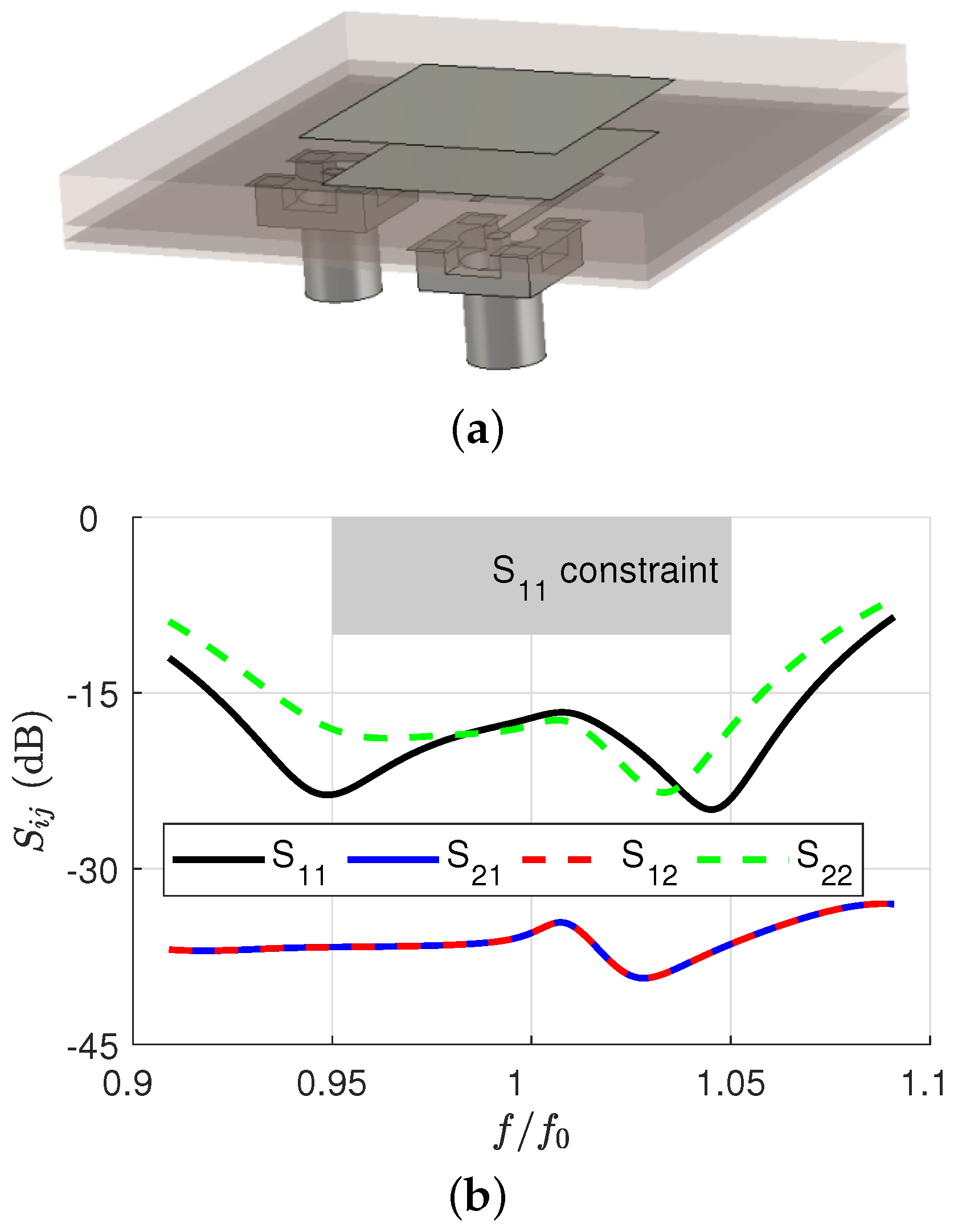
3.2. Full-Wave Results

The aforementioned antenna, that is shown in Figure 5a, consists of a dual-polarized aperture-coupled stacked patch made of three dielectric substrates. On the bottom of the lower substrate (Rogers Kappa438) two printed microstrip lines are used to excite two slots on the top of the same substrate. The plane where the slots are located is also used as a ground plane. On the lower part of the upper substrate there is a parasite patch, slightly smaller than the main patch, printed on the top of the same layer. Both upper and middle dielectric layers are realized with a Taconic TLX-8 laminate.
The radiating element was simulated in CST [24] in a 2-D periodic environment, in order to take into account the coupling effects that occur in a 2-D array. Coaxial feeders, excited in their fundamental TEM mode, were simulated to properly account for their effect in the antenna design. Two wave ports are necessary to properly excite both horizontal and vertical polarization, referred to, respectively, as the H port and V port from now on. The S-parameters results obtained from the simulation of the optimized antenna are shown in Figure 5b. The isolation between ports is rather satisfactory, with values below 30 dB, as well as a reflection coefficient that is well below 10 dB in the frequency range of interest, showing double-resonance behavior related to the presence of the main and parasitic patches of the proposed antenna structure.
In Figure 6, the radiation patterns are shown on the principal planes, and as expected from the reflection coefficients a low cross-polarization level and a symmetric co-polar pattern are obtained for both the H- and V-port excitations. To complete the picture, full-wave 3-D radiation patterns for the co-polar and cross-polar components of both H and V port are shown in Figure 7. A detailed view of the resulting antenna is also shown in Figure 8, whereas in Table 1 a list of the various design parameters is reported.

4. Sub-Array Demonstrator

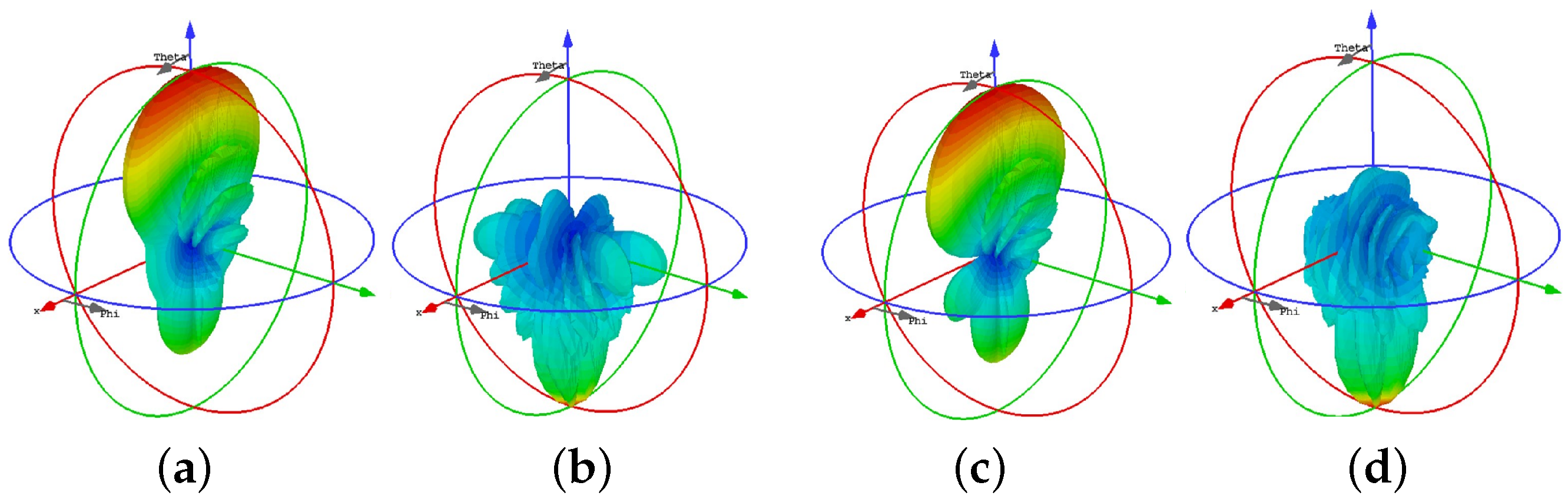
4.1. Full-Wave Results

The radiating element analyzed in the previous section is here used on a 2 × 8 array to realize a demonstrator. This analysis is particularly useful to understand if the unit-cell simulation results (that emulate an infinite-array environment) are consistent with a finite-array simulation setup. The simulation setup is similar to the one described in Section 3, but now the finite 2 × 8 array is simulated replacing the periodic boundary conditions with the radiation boundary conditions.
In Figure 9, the F-parameters obtained from the 2 × 8 array simulation are shown. The F-parameters are used to calculate antenna coupling coefficient sources in the case of simultaneous excitation, when is not possible to apply the general S-parameter definition anymore, and they can therefore be considered as active scattering parameters. In particular, F hh ( vv ) -parameters refers to the reflection coefficient of a port V(H) when all the other ports H(V) are excited, while the F hv ( vh ) -parameters refers to the isolation between the ports H(V) when all the others V(H) are excited. In particular, in the f min f max band the F hh - and F vv -parameters are well below 10 dB, and have a similar behavior to the reflection coefficients obtained from the unit cell simulation for both H and V ports. The same holds for the F hv - and F vh -parameters, that are similar to the transmission coefficients values obtained from the unit-cell simulation. The good agreement between the F-parameters of the array simulation with the S-parameters of the unit-cell simulation demonstrate that the latter takes into account very well the mutual coupling effects.
Moreover, in Figure 10 and Figure 11 the 1-D and 3-D far-field radiation patterns are shown, respectively. It can be noticed that the radiation pattern of the array is squeezed along the array axis due to the array factor. On the transverse axis, the total pattern remains almost unaffected with respect to the element pattern provided by the unit-cell. In all cases, the cross-polar values remain mostly below 20 dB, as expected from the F-parameters.

4.2. Experimental Results

Two prototypes of this 2 × 8 array were fabricated and used to implement a total 4 × 8 array for the measurement setup. The prototypes were placed on a metallic plane properly shaped, and two plexiglass bars were used to secure the two prototypes on the metallic support; see Figure 12a. For that reason, two columns of radiating elements were unavailable, and the array under test was a 4 × 6 array. The measurement setup is shown in Figure 12b, with all the measurements performed in an anechoic chamber.
The measured S i j -parameters are shown in Figure 12c for both the V and H ports, labeled as port 1 and port 2, respectively. The measurements show a frequency shift in the resonance, that is centered to f ˜ 0 = f 0 0.09 f 0 instead of f 0 . However, a fractional bandwidth of 10 % is achieved between f ˜ min = f min 0.09 f 0 and f ˜ max = f max 0.09 f 0 , and the isolation between ports is lower than 30 dB.
The frequency shift can be attributed to different aspects:
  • An important PCB curvature has been observed. This is due to the manufacturing process, and at the design frequency this issue can affect the antenna gain and the S i j -parameters;
  • Possible variations in the dielectric constant with respect to the one shown in the data sheet of the materials;
  • Possible interactions between the metallic support and the radiating elements. These metallic parts are very near to the radiating board, and their effect could be not negligible.
Moreover, the expected higher-frequency resonance in the reflection coefficients for both the H and V ports is deteriorated. This effect is most likely due to the curvature of the PCB caused by the lamination process used to stack the multiple layers.
With this setup, it is possible to evaluate the total pattern from the active reflection coefficient. As is known, the total pattern can be obtained by pattern multiplication between the array factor and the active element pattern G e , act , which in turn is related to the active reflection coefficient Γ act for every scan angle θ 0 , ϕ 0 through the relation [25]
G e , act ( u 0 , v 0 ) = 4 π cos θ 0 p x p y λ 2 ( 1 | Γ act ( u 0 , v 0 ) | 2 )
where p x and p y represent the periodicity of the array along the x- and y-axis, respectively, with u 0 = sin θ 0 cos ϕ 0 and v 0 = sin θ 0 sin ϕ 0 .
The results obtained with (12) from the measurement of the scattering parameters are shown in Figure 13, whereas in Figure 14 are shown the principal planes of the active element pattern for both polarizations, and the gain plot versus frequency at broadside for both polarizations. From these results it can be seen that the active element gain has a quite flat and regular shape in the u v plane and a peak value near to the theoretical expected value in the f ˜ min f ˜ max band. The main reason for this behavior is due to the frequency shift reported in Figure 12b and Figure 14, where the peak gain and the minimum of the reflection coefficient are located around f ˜ 0 .

5. Conclusions

A planar AESA capable of producing a pencil beam with invariant sidelobe level over a wide angular range and at any frequency in C band has been designed with fully analytical techniques. An efficient MATLAB implementation of the Tseng–Cheng technique is presented that looks particularly attractive for realizing a software-defined-radar (SDR) interface for real-time control of the beamforming network. The radiating performance of a case study is analyzed in detail, showing the effects of a reduction in the filling factor. A smaller 4 × 6 demonstrator has been fabricated and measured to test the main radiating performance of the proposed antenna architecture. The flexibility of the polarization control, the low level of cross-polarization, and the good isolation between ports over a 10 % fractional bandwidth make this prototype attractive for future SDR applications.

Author Contributions

Conceptualization, W.F. and A.G.; methodology, W.F. and A.G.; software, W.F.; validation, N.R., L.I. and W.F.; writing—original draft preparation, W.F. and N.R.; writing—review and editing, W.F., N.R., L.I. and A.G.; supervision, T.M., A.M.F. and A.G.; funding acquisition, A.M.F. and A.G. All authors have read and agreed to the published version of the manuscript.

Funding

This research was funded by Leonardo S.p.A. under the contract COLB-CTR-2017-009-A.

Institutional Review Board Statement

Not applicable.

Informed Consent Statement

Not applicable.

Data Availability Statement

The datasets presented in this article are not readily available because the data are part of an ongoing study. Requests to access the datasets should be directed to nicholas.ricciardella@leonardo.com.

Acknowledgments

This work has been developed under the contract COLB-CTR-2017-009-A between Leonardo S.p.A. and Sapienza University of Rome.

Conflicts of Interest

The authors declare no conflicts of interest. The funders had no role in the design of the study; in the collection, analyses, or interpretation of data; in the writing of the manuscript; or in the decision to publish the results.

References

  1. Fulton, C.; Yeary, M.; Thompson, D.; Lake, J.; Mitchell, A. Digital Phased Arrays: Challenges and Opportunities. Proc. IEEE 2016, 104, 487–503. [Google Scholar] [CrossRef]
  2. Kwag, Y.K.; Jung, J.S.; Woo, I.S.; Park, M.S. Modern software defined radar (SDR) technology and its trends. J. Electromagn. Eng. Sci. 2014, 14, 321–328. [Google Scholar] [CrossRef]
  3. Debatty, T. Software defined radar a state of the art. In Proceedings of the 2nd International Workshop on Cognitive Information Processing (CIP), Elba, Italy, 14–16 June 2010; pp. 253–257. [Google Scholar]
  4. Ciociola, A.; Infante, L.; Ricciardella, N.; Solimene, R.; Felaco, M.; Pellegrini, G. Digitally Synthesized Antenna Test Bench for Next Generation Phased Array Systems. In Proceedings of the IEEE International Conference Phased Array Systems & Technology, Waltham, MA, USA, 11–14 October 2022; pp. 1–6. [Google Scholar] [CrossRef]
  5. Castillo-Rubio, C.F.; Pascual, J.M. Current Full Digital Phased-Array Radar developments for Naval applications. In Proceedings of the 2019 IEEE International Symposium on Phased Array System &Technology (PAST), Waltham, MA, USA, 15–18 October 2019; pp. 1–6. [Google Scholar] [CrossRef]
  6. Capria, A.; Petri, D.; Moscardini, C.; Conti, M.; Forti, A.C.; Massini, R.; Cerretelli, M.; Ledda, S.; Tesi, V.; Dalle Mese, E.; et al. Software-defined Multiband Array Passive Radar (SMARP) demonstrator: A test and evaluation perspective. In Proceedings of the OCEANS 2015, IEEE, Genova, Italy, 18–21 May 2015; pp. 1–6. [Google Scholar]
  7. Capria, A.; Giusti, E.; Moscardini, C.; Conti, M.; Petri, D.; Martorella, M.; Berizzi, F. Multifunction imaging passive radar for harbour protection and navigation safety. IEEE Aerosp. Electron. Syst. Mag. 2017, 32, 30–38. [Google Scholar] [CrossRef]
  8. Jamil, K.; Alam, M.; Hadi, M.A.; Alhekail, Z.O. A multi-band multi-beam software-defined passive radar. Part I: System design. In Proceedings of the Radar 2012, Glasgow, UK, 22–25 October 2012; pp. 64–67. [Google Scholar]
  9. Jamil, K.; Alam, M.; Hadi, M.A.; Alhekail, Z.O. A multi-band multi-beam software-defined passive radar. Part II: Signal processing. In Proceedings of the Radar 2012, Glasgow, UK, 22–25 October 2012; pp. 72–75. [Google Scholar]
  10. Saeidi-Manesh, H.; Karimkashi, S.; Zhang, G.; Doviak, R.J. High-isolation low cross-polarization phased-array antenna for MPAR application. Radio Sci. 2017, 52, 1544–1557. [Google Scholar] [CrossRef]
  11. Saeidi-Manesh, H.; Zhang, G. Low cross-polarization, high-isolation microstrip patch antenna array for multi-mission applications. IEEE Access 2018, 7, 5026–5033. [Google Scholar] [CrossRef]
  12. Saeidi-Manesh, H.; Zhang, G. High-isolation, low cross-polarization, dual-polarization, hybrid feed microstrip patch array antenna for MPAR application. IEEE Trans. Antennas Propag. 2018, 66, 2326–2332. [Google Scholar] [CrossRef]
  13. Tseng, F.I.; Cheng, D.K. Optimum scannable planar arrays with an invariant sidelobe level. Proc. IEEE 1968, 56, 1771–1778. [Google Scholar] [CrossRef]
  14. Rocca, P.; Oliveri, G.; Mailloux, R.J.; Massa, A. Unconventional phased array architectures and design methodologies—A review. Proc. IEEE 2016, 104, 544–560. [Google Scholar] [CrossRef]
  15. Cheng, D.K. Optimization techniques for antenna arrays. Proc. IEEE 1971, 59, 1664–1674. [Google Scholar] [CrossRef]
  16. Kim, Y.; Elliott, R. Extensions of the Tseng–Cheng pattern synthesis technique. J. Electromagn. Waves Appl. 1988, 2, 255–268. [Google Scholar] [CrossRef]
  17. Elliot, R.S. Antenna Theory and Design; John Wiley & Sons: Hoboken, NJ, USA, 2006. [Google Scholar]
  18. Balanis, C.A. Antenna Theory—Analysis and Design; John Wiley & Sons, Inc.: Hoboken, NJ, USA, 2005. [Google Scholar]
  19. Mailloux, R.J. Phased Array Antenna Handbook; Artech House: Washington, DC, USA, 2005. [Google Scholar]
  20. Waterhouse, R. Microstrip Patch Antennas: A Designer’s Guide; Springer Science & Business Media: Berlin/Heidelberg, Germany, 2013. [Google Scholar]
  21. Mishra, P.K.; Jahagirdar, D.R.; Kumar, G. A Review of Broadband Dual Linearly Polarized Microstrip Antenna Designs with High Isolation [Education Column]. IEEE Antennas Propag. Mag. 2014, 56, 238–251. [Google Scholar] [CrossRef]
  22. Ghorbani, K.; Waterhouse, R. Dual polarized wide-band aperture stacked patch antennas. IEEE Trans. Antennas Propag. 2004, 52, 2171–2175. [Google Scholar] [CrossRef]
  23. Yang, F.; Rahmat-Samii, Y. Microstrip antennas integrated with electromagnetic band-gap (EBG) structures: A low mutual coupling design for array applications. IEEE Trans. Antennas Propag. 2003, 51, 2936–2946. [Google Scholar] [CrossRef]
  24. SIMULIA CST Studio Suite. Dassault Systemes; SIMULIA CST Studio Suite: Dearborn, MI, USA, 2023. [Google Scholar]
  25. Pozar, D. The active element pattern. IEEE Trans. Antennas Propag. 1994, 42, 1176–1178. [Google Scholar] [CrossRef]
Figure 1. Map of the amplitude coefficients of a 40 × 40 array for the design specifications on the beam given in the text through the Tseng–Cheng technique.
Applsci 14 06015 g001
Figure 2. Color maps of | AF | 2 / | AF | max 2 vs. θ and ϕ , for (a) an ideal Tseng–Cheng technique, (bd) a Tseng–Cheng technique neglecting coefficients with amplitudes below 0.01 , 0.05 , and 0.1 , respectively, when θ 0 = 60 , ϕ 0 = 45 . The dotted-dashed lines represent the 30 dB iso-lines of the contour plot. Parameters of the Tseng–Cheng technique and of the array are reported in the text. (eh) The radiated power density normalized to the absolute maximum (i.e., | AF | 2 / | AF | max 2 ) along the principal planes (in black solid lines and dashed gray lines, the plane ϕ = ϕ 0 , and the orthogonal one, respectively), for the same cases analyzed in (ad), respectively.
Applsci 14 06015 g002
Figure 3. (a) Beam squint Δ θ and (b) gain loss vs. f in the range f min = 0.95 f 0 , f max = 1.05 f 0 . In (a) numerical (theoretical) results are reported with solid black (dashed gray) lines.
Applsci 14 06015 g003
Figure 4. The beamwidths along the principal planes Θ h (in black) and Ψ h (in gray) vs. f in the range f min f m a x . Numerical (theoretical) results are reported with solid (dashed) lines.
Applsci 14 06015 g004
Figure 5. (a) Proposed antenna, (b) S-parameters of the optimized radiating element.
Applsci 14 06015 g005
Figure 6. (a,d) Main cuts of the radiation pattern for the optimized radiating element. (a,b) refer to H-port excitation; (c,d) refer to V-port excitation. (a,c) show the ϕ = 0 cuts, whereas (b,d) show the ϕ = 90 cuts.
Applsci 14 06015 g006
Figure 7. (ad) Radiation patterns for (a,b) horizontal polarization, (c,d) vertical polarization at f 0 . In (ac), co-polar component; in (bd), cross-polar component.
Applsci 14 06015 g007
Figure 8. (ac) Detailed antenna structure. (a) Front view and cross sections at different heights. (b) Back view from the ground plane and feeding structure. (c) Back view from SMA connectors.
Applsci 14 06015 g008
Figure 9. 2 × 8 array F-parameters of the optimized radiating element.
Applsci 14 06015 g009
Figure 10. (ad) Main cut of the radiation patterns for the 2 × 8 array. (a,b) show results while the H port is excited, (c,d) while the V port is excited. In (ac), the ϕ = 0 cut is plotted; in (bd), the ϕ = 90 cut is plotted.
Applsci 14 06015 g010
Figure 11. (ad) Radiation patterns for (a,b) horizontal polarization, and (c,d) vertical polarization at f 0 . In (ac), co-polar component; in (bd), cross-polar component.
Applsci 14 06015 g011
Figure 12. (a) Array demonstrator; (b) measurement setup. The inset in the top-right corner shows the feeding mechanism. (c) Measured S-parameters.
Applsci 14 06015 g012
Figure 13. (ac) Gain measurements on the u v plane for H polarization at (a) f ˜ min , (b) f ˜ 0 , and (c) f ˜ max . (df) As in (ac) but for V polarization.
Applsci 14 06015 g013
Figure 14. Gain obtained from the Γ a c t measurements for the three main frequencies ( f ˜ min , f ˜ 0 , f ˜ max ) on the planes (a) ϕ = 0 and (b) ϕ = 90 for H polarization. In (c,d), as in (a,b) but for V polarization. (e,f) The gain in dB obtained from Γ a c t measurements for θ = 0 versus the expected gain for H and V polarization, respectively.
Applsci 14 06015 g014
Table 1. Design parameters for the radiating element.
Substrates/Patch/ConnectorsSlotsStrips
ParameterValue [mm]ParameterValue [mm]ParameterValue [mm]
p26.98 d x Hslot 12.42 d x Hstrip 4.80
h 1 0.51 d y Hslot 10.00 d y Hstrip 13.05
h 2 0.79 d x Vslot 6.02 d x Vstrip 8.55
h 3 2.36 d y Vslot 12.56 d y Vstrip 4.80
w p 1 12.9 w Hslot 1.84 w Hstrip 0.9
h p 1 12.9 h Hslot 1.84 l Hstrip 8.87
w p 2 14.5 w Hslit 0.26 w Tstrip 0.55
h p 2 14.5 l Hslit 3.29 l Tstrip 6.00
d x H 5.50 w Vslot 1.85 w Vstrip 0.90
d y H 13.49 h Vslot 1.85 l Vstrip 11.37
d x V 9.00 w Vslit 0.15
d y V 5.50 l Vslit 2.25
Disclaimer/Publisher’s Note: The statements, opinions and data contained in all publications are solely those of the individual author(s) and contributor(s) and not of MDPI and/or the editor(s). MDPI and/or the editor(s) disclaim responsibility for any injury to people or property resulting from any ideas, methods, instructions or products referred to in the content.

