Article

Boron Carbonitride Films with Tunable Composition: LPCVD and PECVD Synthesis Using Trimethylamine Borane and Nitrogen Mixture and Characterization

by
Svetlana V. Belaya
1,
Eugene A. Maksimovsky
1,
Vladimir R. Shayapov
1,
Aleksandra A. Shapovalova
1,
Alexey N. Kolodin
1,
Andrey A. Saraev
2,
Igor P. Asanov
1,
Maxim N. Khomyakov
3,
Irina V. Yushina
1,
Aleksandr G. Plekhanov
1,
Veronica S. Sulyaeva
1 and
Marina L. Kosinova
1,*
1
Nikolaev Institute of Inorganic Chemistry SB RAS, 3, Acad. Lavrentiev Ave., Novosibirsk 630090, Russia
2
Boreskov Institute of Catalysis SB RAS, 5, Acad. Lavrentiev Ave., Novosibirsk 630090, Russia
3
Institute of Laser Physics SB RAS, 15B, Acad. Lavrentiev Ave., Novosibirsk 630090, Russia
*
Author to whom correspondence should be addressed.
Appl. Sci. 2023, 13(8), 4959; https://doi.org/10.3390/app13084959
Submission received: 10 March 2023 / Revised: 7 April 2023 / Accepted: 11 April 2023 / Published: 14 April 2023
(This article belongs to the Collection Organic Corrosion Inhibitors and Protective Coatings)

Abstract

:
This study reports the chemical vapor deposition of amorphous boron carbonitride films on Si(100) and SiO2 substrates using a trimethylamine borane and nitrogen mixture. BCxNy films with different compositions were produced via variations in substrate temperature and type of gas-phase activation. The low-pressure chemical vapor deposition (LPCVD) and plasma-enhanced chemical vapor deposition (PECVD) methods were used. The “elemental composition—chemical bonding state—properties” relationship of synthesized BCxNy was systematically studied. The hydrophilicity, mechanical, and optical properties of the films are discussed in detail. The composition of films deposited by the LPCVD method at temperatures ranging from 673 to 973 K was close to that of boron carbide with a low nitrogen content (BCxNy). The refractive index of these films changed in the range from 2.43 to 2.56 and increased with temperature. The transparency of these films achieved 85%. LPCVD films were hydrophilic and the water contact angles varied between 53 and 63°; the surface free energy was 42–48 mN/m. The microhardness, Young’s modulus and elastic recovery of LPCVD films ranged within 24–28 GPa, 220–247 GPa, and 70–74%, respectively. The structure of the PECVD films was close to that of hexagonal boron nitride, and their composition can be described by the BCxNyOz:H formula. In case of the PECVD process, the smooth films were only produced at low deposition temperatures (373–523 K). The refractive index of these films ranged from 1.51 to 1.67. The transparency of these films achieved 95%; the optical band gap was evaluated as 4.92–5.28 eV. Unlike LPCVD films, they were very soft, and their microhardness, Young’s modulus and elastic recovery were 0.8–1.4 GPa, 25–26 GPa, and 19–28%, respectively. A set of optimized process parameters to fabricate LPCVD BCxNy films with improved mechanical and PECVD films with high transparency is suggested.

1. Introduction

In recent decades, much attention has been paid to the study of materials with a layered structure such as carbon, boron nitride (BN), boron carbonitride (BCxNy), transition metal dichalcogenides, etc. due to their remarkable functional performance [1,2,3,4]. Modification of these materials by functionalizing the surface, changing the architecture (1D, 2D, 3D), and integrating with other materials, including nanoparticles, leads to a change in their physical properties, different from what was originally, and expands the areas of their application. For example, 2D graphene has limited application potential in optoelectronics because of its low light absorptivity and gapless property. 3D graphene has shown its application in Si-based near infra-red tunneling heterojunction photodetectors [5] and the structure of 3D graphene with germanium-on-insulator can be used as dual-enhanced photodetectors [6]. Using another way to modify graphene, namely the use of PbS quantum dots on N, S decorated graphene made it possible to create graphene–quantum dot phototransistors [7]. It is also known that BCN-based materials have a wide variety of architectures such as nanotubes, nanoribbons, nanosheets, nanowalls, foams, and nanoscrolls [3]. It should be emphasized that in the case of boron carbonitride, the ability to vary the elemental composition expands the possibilities of the above methods for modifying the functional properties of this material. However, searching for ways to achieve different compositions of BCxNy remains an important challenge.
As is well known, binary and ternary compounds of various structures and stoichiometry can be formed in the B–C–N system. Although boron carbide is usually denoted as B4C, it has a wide area of homogeneity, and the carbon concentration, according to different authors, can be the following: 9–19 at.% C [8], 9–20 at.% C [9], and 8.6–21.6 at.% C [10], where boron carbide exists as a stable single phase. Boron carbide has a complex structure based on B12 or B11C icosahedra and C–B–C, C–B–C, C–B–B, or B⊗B (⊗—vacancy) chains [11]. Boron nitride of hexagonal modification (h-BN) has a layered structure isoelectronic to graphite [12,13]. The ternary h-BCxNy is formed on the basis of hexagonal structures of boron nitride and carbon. The unquenchable interest in BCxNy materials, including nanostructures, is due to the ability to tune their physical characteristics by changing the stoichiometry and bonding configurations of these compounds [3]. Since h-BN is an insulator and the graphite is a semimetal, h-BCxNy compounds are of interest for optoelectronics as materials with an adjustable band gap and tunable optical and electrical properties [14,15]. Materials based on BCxNy, having low atomic masses and covalent bonds, being simultaneously light and high strength, exhibit a hardness in a wide range of values [3,15,16]. It should be noted that h-BN [17,18], B4C [19], h-BCxNy [20,21] and BCxNy/graphene [22] coatings with high thermal and chemical stability have proven their effectiveness in metallic corrosion resistance.
The steady interest in BCxNy films is due not only to their remarkable properties but also to the fact that it is not a simple object of both physicochemical research and technological developments. The ratio of the elements’ content and the local environment of atoms in the films can be changed by applying various methods of deposition and varying the conditions of formation. One of the widely used methods of BCxNy film synthesis is chemical vapor deposition (CVD) including low-pressure CVD (LPCVD), plasma-enhanced radio frequency CVD (RF-PECVD), plasma-enhanced microwave frequency CVD (MW-PECVD), laser CVD (LCVD), electron cyclotron resonance plasma enhanced CVD, isothermal CVD and glow discharge plasma-assisted CVD [3,16]. It is important to note that the properties of the BCxNy films depend on a type of CVD process, the precursors’ nature, their concentration in the initial gas mixture, the type of additional gases, as well as on the reactor chamber geometry, the substrate temperature, the total pressure of the gas mixture in the reactor, the parameters of the plasma generator (in case of PECVD processes), laser wavelength and power (in case of LCVD processes), and other deposition parameters appropriate to a particular method.
To obtain BCxNy films in CVD processes, volatile boron fluoride, boron chloride, and diborane can be used as a source of boron and sources of carbon (hydrocarbons or CCl4) and nitrogen (N2, NH3), which sometimes require separate supply channels [3,23,24]. It should be noted that the aforementioned precursors are toxic and pyrophoric substances, the danger of which increases at high operating temperatures. A limited number of works [23,25] dealt with the use of diborane B2H6 and dimethylamine (CH3)2NH, which contains two other components (nitrogen and carbon), or nitrogen with trimethylborane B(CH3)3 containing both carbon and boron in the LCVD processes. The alternative way of synthesis of BCxNy films is through the use of organoboron compounds with various compositions and structures. They are single source-precursors containing all the necessary elements in one molecule. These compounds, including alkylamine boranes, are of special interest because the molecular structure of the initial organoboron precursor affects the chemical and phase compositions and the microstructure of deposited films [26,27,28,29,30]. They are stable under normal conditions, less toxic than volatile binary boron compounds, non-combustible, and relatively cheap [31]. One of them is trimethylamine borane (CH3)3N·BH3 (TMAB) [32,33]. Previously, a number of works has already been carried out using TMAB as a precursor. Table 1 contains the data on the conditions of the CVD syntheses of the BCxNy films from TMAB and their chemical composition and functional properties. As one can see, the main attention was paid to LPCVD and RF-PECVD methods. To date, there are relatively few studies devoted to the MW-PECVD technique. An important advantage of using plasma-activated processes is a decrease in the film synthesis temperature. The literature analysis and results summarized in Table 1 show that special attention was devoted to the determination of elemental composition, chemical structure and mechanical characteristics of BCxNy films depending on the film growth conditions.
BCxNy films obtained by chemical vapor deposition are usually amorphous which was demonstrated by the conventional X-ray diffraction method. Therefore, it is generally accepted to judge their structure by the nearest atomic environment, which can be studied using spectroscopic methods such as IR-Fourier, Raman, X-ray photoelectron spectroscopy (XPS), electron energy loss spectroscopy, X-ray absorption near edge structure spectroscopy, synchrotron radiation-based total reflection X-ray fluorescence analysis combined with near-edge X-ray absorption fine structure spectroscopy (TXRF-NEXAFS), and some others. The first three of these methods are the most common and, when used together, provide information on interatomic bonds in the film’s material and its local chemical structure.
The elemental composition of films is significantly affected by the method of gas-phase activation. As a result of the thermal decomposition of TMAB, the boron content in the films is high, while the nitrogen content is negligible. Using PECVD processes significantly decreases the boron content and increases the content of carbon and nitrogen. The films, prepared by LPCVD and PECVD from the TMAB + He mixture at 723 K, had the compositions of B0.72C0.23N0.04O0.01 and B0.33C0.46N0.21O0.01, respectively [37]. The authors also reported on the effect of the type of additional gases, such as H2, He, N2, and NH3, the partial pressure of ammonia, and the substrate temperature on the composition of the deposited films. In the work [36], the BCxNy films deposited by LPCVD method at 973 K were characterized by XPS and TXRF-NEXAFS. The composition of the films produced from TMAB and its mixtures with He and N2 is close to a B–C bond containing compound with an atomic relation of [B]:[C] = 1:1. The addition of ammonia led to an increase in the nitrogen content in the films and the formation of a compound with an atomic ratio of [B]:[C]:[N] = 1:1:1.
For BCxNy films deposited by the PECVD method at 673 K [37], the introduction of ammonia reduces the carbon content, increases the nitrogen content, and leads to the formation of B–N bonds.
All authors note the presence of oxygen in the films. Its content is highly dependent on the method of film formation. In LPCVD films, the oxygen content is equal to 1–4 at.%. Films deposited in plasma-stimulated processes have an oxygen content up to 15 at.% and up to 51 at.% in the case of RF PECVD and MW PECVD, respectively (Table 1).
Despite the above-mentioned studies with respect to the use of mixtures of TMAB with He, H2, and NH3, there is a lack of systematic data concerning the influence of nitrogen addition on the properties of BCxNy films. There are several works on the use of the TMAB + N2 mixture in the MW PECVD process [41]. Ammonia is most often used to introduce nitrogen into films. It is known that nitrogen is less reactive from these two nitrogen-containing gases, due to the stronger N≡N than N–H binding [42]. However, the advantage of nitrogen is the absence of hydrogen in its molecule [43].
As can be seen from Table 1, the authors paid attention to the study of the mechanical properties (hardness and Young’s modulus) and the optical ones (refractive index and transmittance) of BCxNy films. The maximum hardness value of 34 GPa was obtained for LPCVD films using TMAB + He mixture. The refractive index can be varied over a wide range from 1.6 to 2.8 by varying the films’ composition. Highly transparent films can be obtained in the RF PECVD processes using TMAB + NH3 mixture. It should be emphasized that information on the values of the optical band gap, wettability, and surface free energy is absent for films deposited using TMAB.
The present paper focuses on the investigation of a synthesis of BCxNy films by LPCVD and RF PECVD methods using the TMAB+N2 initial mixture and on the study of the types of chemical bonds in films and physical properties depending on the chemical structure. In the present work, the synthesis temperature was chosen as a variable parameter.

2. Materials and Methods

BCxNy films were obtained on polished n-type Si(100) substrates, n-type phosphorus-doped Si(100) substrates with a resistivity of 4.5 Ω·cm, with a thickness of 470 μm and an area of 1.0 × 1.0 cm2, by two methods such as LPCVD and RF PECVD (13.56 MHz, 50 W) using the equipment presented in [44]. Trimethylamine borane (CH3)3N·BH3 (TMAB) (97% pure, Sigma-Aldrich, Merck Ltd., Darmstadt, Germany) thermostated at a temperature of 273 K was a source of B, C, and N. Nitrogen gas of high purity was used as a reagent gas. The ratio of partial pressures of TMAB to nitrogen was PTMAB:PN2 = 1:1. The value of the base pressure in the reactor chamber was 4 × 10⁻³ Torr. The variable parameter was the temperature in the substrate zone (Tdep), which varied in the ranges of 673–973 K and 373–873 K for films obtained by the LPCVD and PECVD methods, respectively. The reproducibility of the deposition processes was confirmed by a series of parallel experiments. Immediately before the synthesis of the films, the substrates were degreased successively in trichloroethylene and acetone, then etched successively in ammonia-peroxide, in hydrochloric acid-peroxide solutions, and in concentrated hydrofluoric acid, according to the standard procedure. Fused silica plates were used as substrates for the UV-Vis transmittance study. For them, only the degreasing procedure was carried out. Degreasing and each stage of substrate etching ended with washing with deionized. Finally, the substrates were dried in a nitrogen flow at 353 K.
The elemental composition of the films was determined by X-ray energy dispersive spectroscopy (EDX) using a JSM-6700F (Jeol, Tokyo, Japan) scanning electron microscope (SEM), with a Quantax 200 (Bruker, Berlin, Germany) EDX attachment at an accelerating voltage of 3 keV [45]. The surface morphology of the films was studied using SEM. The topology of the samples was studied using a Ntegra Prima II atomic force microscope (AFM) (NT-MDT, Zelenograd, Russia) in the semicontact mode. An HA_NC (A) probe was used with the following parameters: probe length of 123 µm, width of 34 µm, thickness of 3 µm, curvature radius of 10 nm, force constant of 17 N/m, resonant frequency of 230 kHz. The calculation of the root mean square surface roughness (RMS) was carried out using the Nova SPM software according to the standard ISO 4287-1.
X-ray diffraction patterns of the samples were recordered on a Bruker D8 Advance diffractometer (Bruker, Berlin, Germany) using CuKα radiation with LYNXEYE XE-T linear detector in the range of 2θ = 5–65° with 2θ step of 0.03° at an accumulation of 5 s per point.
The thickness d and refractive index n of the films were calculated using data of monochromatic ellipsometry using an LEF-3M (Instrument-making plant, Feodosiya, USSR) scanning null laser ellipsometer equipped with a He-Ne laser (λ = 632.8 nm). The measurements were carried out at 5 incidence angles: 50°, 55°, 60°, 65°, and 70°. The thickness of the films obtained by the PECVD method at Tdep = 573–873 K was estimated from the SEM micrograph of a cross-section of the BCxNy/Si(100) structure. The error in determining n was 0.02–0.04.
The chemical structure of the films was studied using Fourier transform infrared (FT-IR) spectrometry in absorption mode with a SCIMITAR FTS 2000 spectrometer (Digilab, Hopkinton, MA, USA). The spectral range between 375 and 4000 cm−1 was probed with a resolution of 2 cm−1. A Si(100) substrate after standard chemical treatment was used as a reference sample. In order to compare the peaks’ intensities, the absorbance values were normalized by each film’s thickness.
The Raman spectra of the films were obtained on a LabRAM HR Evolution Raman spectrometer (Horiba, Kyoto, Japan), equipped with a liquid nitrogen-cooled Symphony II CCD detector, in backscattering geometry (Ar laser, λ = 514.5 nm).
UV—Vis transmission spectra were recorded using a Shimadzu UV-3101PC scanning spectrophotometer (Shimadzu, Kyoto, Japan) in the wavelength range of 190–2200 nm. Ellipsometric measurements of LPCVD BCxNy films were performed on an ELLIPS-1991 spectral ellipsometer (ISP SB RAS, Novosibirsk, Russia) at a light incidence angle on the sample of 60°. The inverse problem of ellipsometry was solved using the Forouhi-Bloomer dispersion model [46]. As a result, the spectra of the refractive index and the extinction coefficient were obtained depending on the wavelength. The values of the optical band gap were estimated using spectrophotometry and spectral ellipsometry data. The values of the optical band gap were estimated from Tauc’s plot using the equation αhν = A(Eg)2, where h is the Planck constant, ν is the vibration frequency [47]. The absorption coefficient α was calculated using formulas α = 1/dln(1/T) and α = 4πk/λ for spectrophotometry and ellipsometry measurements, respectively.
The study of the chemical composition of the surface of LPCVD films was carried out on a photoelectron spectrometer (SPECS Surface Nano Analysis GmbH, Berlin, Germany). The spectrometer is equipped with a PHOIBOS-150-MCD-9 hemispherical analyzer, an XR-50 source of X-ray characteristic radiation with a double Al/Mg anode. The characteristic radiation Al Kα (hν = 1486.6 eV) was used to record the spectra. To take into account the charging effect of the samples, the C1s spectra of carbon contamination (Eb = 284.8 eV) were used; this peak corresponds to carbon forming C=C/C–H covalent bonds. The relative concentrations of elements were determined based on the integral intensities of XPS lines, taking into account the photoionization cross-section of the corresponding terms [48]. For a detailed analysis, the spectra were decomposed into individual components. Accordingly, after subtracting the background by the Shirley method, the experimental curve was decomposed into a series of lines corresponding to the photoemission of electrons from atoms in various chemical environments. Data processing was carried out using the CasaXPS 2.3.24PR1.0 software package. The shape of the peaks was approximated by a symmetric function obtained by multiplying the Gauss and Lorentz functions.
For PECVD films, the measurements were carried out on a FLEXPS X-ray photoelectron spectrometer (Specs, Berlin, Germany) with a Phoibos 150 electron energy analyzer and a DLD electron detector. The spectra were excited by monochromatic Al Kα radiation. The analyzer transmission energy is 20 eV. The vacuum in the system is ~7.5 × 10⁻¹¹ Torr The electron energy was calibrated with respect to the copper line Cu2p3/2 = 932.6 eV. The spectra were calibrated using the C1s internal standard of carbon (Eb = 284.8 eV). The element concentration was calculated from the area of the peaks, taking into account the electron photoionization cross-section and the electron mean free path. The approximation of a uniform distribution of elements at the depth of analysis was used. The depth of analysis was estimated based on the exponential decay of the signal with respect to depth and was 3λ, where λ is the electron-free path without inelastic collisions. The value of λ was calculated using the TPP2M formula [49] and lies in the region of 3.2–2.6 nm for the B1s, C1s, N1s, and O1s lines.
The contact angles on the films were measured using an OCA 15 PRO device (Dataphysics, Filderstadt, Germany) equipped with a measuring video system with a USB camera and a high-aperture measuring lens with an adjustable viewing angle. All measurements were performed under standard conditions in a thermostated box (T = 298 ± 2K and p = 750 Torr). The needle diameter was 0.51 mm. Distilled water and diethylene glycol (DEG) were used as test liquids with different polarities. The droplet volume was constant and equal to ~1.5 μL. The contact angles (CA) were measured in the sessile drop mode. The drop profile shape of the samples was determined in two ways: the Young-Laplace method and the ellipse approximation method. The final values of the contact angles were calculated as the average of three measurements. The calculation of the surface free energy (SFE) was carried out using two methods: the Newman (equations of state) [50] and Owens-Wendt [51]. Additional detailing of the SFE characteristics of the samples with the calculation of the polar and dispersive components was carried out using the Owens-Wendt method.
The microhardness (H), Young’s modulus (E), coefficient of elastic recovery (R) of the BCxNy films, as well as the adhesion of the films to the Si(100) substrate were determined using nanoindentation measurements and sclerometry test according to ISO 14577 with scanning nano-hardness tester NanoScan-3D (TISNCM, Troitsk, Moscow, Russia). The procedure for measuring and calculating the values of the mechanical properties of films is given in [52].
The applied load was gradually increased from 1 to 70 mN. Each sample was probed at 10 different locations. Average values of both hardness and elastic modulus were calculated from the curves of the dependence of load from penetration depth with the method proposed by Oliver & Pharr. The dependence of the effective hardness of the “film-substrate” system on the depth of the indenter penetration was analyzed. The obtained dependence was approximated using Korsunsky’s model [53] for averaging the experimental data and determining the film’s hardness without the substrate influence. The typical dependences of hardness and Young’s modulus on the indentation depth for the BCxNy sample are shown in Figure S1.
The adhesive strength of the film was evaluated by scratching the sample surface with a pyramidal indenter of the Berkovich type forward with the edge and the face of the indenter at a continuously increasing load from 0.1 to 100 mN. The AFM method was used to control the residual trace topology after the scratching test.

3. Results and Discussion

The growth of BCxNy films using both LPCVD and PECVD techniques was investigated by studying the role of a type of CVD processes and deposition temperature on the deposition rate, surface morphology, elemental composition, chemical bonding state, optical, mechanical properties and wettability of the as-grown films. Trimethylamine borane, which contains all necessary elements for BCxNy film formation was used as a single-source precursor. The additional gas was nitrogen.

3.1. Film Deposition Rate

Figure 1 shows the dependencies of the film growth rate on the deposition temperature. In the case of LPCVD films, it increases almost linearly from 1.7 to 6.6 nm/min with an increase in Tdep from 673 to 973 K. These values are comparable with the data of [54] where the growth rate was 3.4–7.9 nm/min. The growth rate of LPCVD films obtained from a mixture of dimethylamine borane and ammonia increased from 0.3 to 4.0 nm/min with an increase in the synthesis temperature from 633 to 773 K [55].
In the case of PECVD films, the curve consists of two sections as Tdep increases from 373 to 523 K, the deposition rate sharply decreases from ~18 to ~5 nm/min, and at temperatures of 523–873 K it reaches a constant value. It should be noted that the use of TMAB + NH3 mixture in similar PECVD process led to lower deposition rates (1–6 nm/min) [38]. The use of dimethylamine borane with ammonia leads to even lower rates (0.5–3.5 nm/min) [56].

3.2. Film Surface Morphology, Topology, and Structure Study

All synthesized films were continuous and uniform. As can be seen from the SEM images presented in Figure 2, the surface of LPCVD films consists of spherical particles 20–40 nm in size and does not change significantly with Tdep in the studied temperature range (Figure 2a). In contrast to them, significant changes in the surface morphology of PECVD films were noticed with the synthesis temperature increasing. The surfaces of films obtained at Tdep = 373–473 K are smooth, homogeneous, and without any features (Figure 2b). There are rounded particles on the film surface synthesized at Tdep = 523 K (Figure 2c). With a further increase in temperature to 673 K, the formation of nanowalls, uniformly distributed over the area of the sample, is observed. [57] (Figure 2d–f). The SEM image of the cross-section of such a structure is shown in Figure 2f. In this work, we limited ourselves to studying the physicochemical and functional properties of smooth films only; films consisting of nanowalls will be the object of study in another work.
Figure 3a–c shows the AFM images of the surface of the LPCVD films. The root-mean-square (RMS) roughness of films deposited at 673, 873, and 973 K is 0.21, 1.33, and 1.54, respectively. The PECVD film obtained at Tdep = 523 K has RMS equal to 1.64 nm (Figure 3d). The data indicates the formation of smooth films.
Previously, we studied the temperature dependence of the RMS roughness of PECVD BCxNy films deposited using a mixture of trimethylborazine and nitrogen. The roughness varied from 0.5 to 2.6 nm with an increase in Tdep from 373 to 973 K [58]. Other authors [55] observed the same trend for LPCVD BCxNy films. An increase in the RMS roughness from 0.3 nm to 0.5 nm with an increase in temperature from 633 K to 773 K was found for films deposited using a mixture of dimethylamine borane and ammonia.
Figure S2 shows the X-ray diffraction patterns of Si(100) substrate, the 190 nm thick film deposited at Tdep = 973 K and the 270 nm thick film deposited at Tdep = 523 K by LPCVD and PECVD, respectively. XRD patterns of films are similar to those of the substrate. They contain no reflexes, which indicates the amorphous nature of these films. The only peak at 2θ = 33° corresponds to the Si(200) forbidden reflection of a substrate [59]. In other studies [40,41], BCxNy films deposited from TMAB were also found to be amorphous.

3.3. Films’ Composition and Chemical Bonding State

The quantitative compositional information on the surface and volume of a layer is a basic measurement of importance to the design and performance diagnosis of thin films. The films’ compositions were evaluated using analysis methods such as energy dispersive, Raman, FTIR and X-ray photoelectron spectroscopy.

3.3.1. EDX Spectroscopy Data

The EDX spectra confirmed the presence of boron, carbon, nitrogen, and oxygen. Experimental chemical maps based on EDX data show uniform elemental distribution over the sample’s site. Figure 4 shows the data for two films obtained by LPCVD (Tdep = 973 K) and PECVD (Tdep = 373 K) and having B0.67C0.24N0.08O0.01 and B0.22C0.36N0.19O0.24 compositions, respectively.
Figure 5 presents the change in the elemental composition of both LPCVD and PECVD films with increasing Tdep. The composition of LPCVD films smoothly changes from B0.80C0.14N0.04O0.02 to B0.67C0.24N0.08O0.01 for the temperature interval from 673 K to 973 K, at this [N]:[B] equal to 0.05–0.01 in these films is two orders of magnitude lower than in the used precursor. Meanwhile, the using a mixture of TMAB with ammonia (PTMAB:PNH3 = 1:1) at Tdep = 973K led to the formation of a film with [N]:[B] close to 1 [36,54] (Table 1), which indicates the inertness of nitrogen compared to ammonia in the process.
It should be noted that all LPCVD films exhibited a small concentration of oxygen which varied within 1–2 at.%. As the temperature rises, the boron content decreases and the carbon and nitrogen contents increase. A similar trend was found in the synthesis of LPCVD BCxNy films from a mixture of triethylamine borane and ammonia. The authors of [60] explained the increase in carbon content at high temperatures by the decomposition of triethylamine molecules into nitrogen and hydrocarbons with a further decomposition of the latter. According to [55], as the substrate temperature increased, the boron concentration also decreased while the nitrogen and carbon concentrations increased for LPCVD BCxNy films deposited from a mixture of dimethylamine borane and argon.
A high percentage of the boron content suggests that the composition of these films is close to boron carbide, the stoichiometry of which can vary within the interval of B4C–B10.1C [8,9,10]. In our case, the [B]:[C] ratio changes from 5.7 to 2.8. It can be assumed that high-temperature films also contain carbon as an elementary phase, which will be confirmed later by Raman spectroscopy.
Plasma-stimulated processes can significantly reduce the film deposition temperature. The Tdep in this case lies in the interval from 373 K to 873 K. The contents of boron and nitrogen in the films synthesized up to Tdep = 573 K increase almost linearly from 22 to 39 at.% and from 19 to 40 at.%, respectively (Figure 5b). While the contents of carbon and oxygen decrease from 36 to 12 at. % and from 24 to 13 at.%, respectively. For the high-temperature films (Tdep > 573 K), the boron content practically does not change, [C] increases to 25 at.%, while [N] and [O] slightly decrease. Based on the previously obtained data on decomposition of organoboron compounds in the PECVD processes, it can be assumed that the increase in the carbon content can be associated with the deposition of graphite-like carbon [38,61]. The ratio of boron to nitrogen in PECVD films is approximately equal to 1, which corresponds to their ratio in the precursor. The high oxygen content in these films should be noted. In this regard, it is more correct to describe the films obtained in PECVD process as BCxNyOz. Oxygen contamination may originate from several sources: (a) not a high vacuum in the reactor chamber of our CVD set-up; (b) the reactions of dangling bonds in the surface layer with atmospheric oxygen or moisture, which may occur after the film exposure to the ambient environment; (c) the etching of the quarts walls of the reactor with the highly reactive species during plasma activated process which resulting in incorporation of the oxygen-containing products into the growing film. It should be emphasized that the method of activation of the gas phase, such as thermal and plasma-stimulated, has a significant effect on the oxygen content in the films. There is the slight oxygen contamination in the LPCVD BCxNy films, while in the PECVD films the oxygen content is much higher and its concentration decreases with increasing synthesis temperature. A similar trend for BCxNy films was obtained in PECVD processes with trimethylamine borane [26] and triethylamine borane [62]. In the case of PECVD processes during the decomposition N-trimethylborazine and N-triethylborazine, the oxygen content in films increased with a decrease in the temperature of the synthesis and the addition of ammonia in the initial gas mixture [63,64]. It was observed in [41] that a decrease in plasma power during MW PECVD with TMAB led to an increase in oxygen content.

3.3.2. FTIR Spectroscopy Data

The FTIR absorption measurements were performed in order to investigate the effect of synthesis conditions on the chemical structure changes of the prepared films.
The interpretation of the IR spectra of the films was carried out using the literature data. It is known that single crystal and polycrystalline rhombohedral B4C have bands at 1090 cm−1 and 1580 cm−1 [65]. The first of them is assigned to B–C vibrations in B11C icosahedra, while the second one corresponds to vibrations of C–B–C chains connecting the icosahedra to each other. There is a series of vibration bands of lower intensities in the region of 700–880 cm−1 in the IR spectrum of a crystalline B4C [66]. The IR spectrum of amorphous boron carbide has a band at 1100 cm−1 that is shifted to 1200 cm−1 for carbon-rich a-BCx films [67]. It is known that in the spectrum of the crystalline h-BN there are bands of in-plane vibrations of boron and nitrogen atoms (B–N) (ν|| = 1367 cm−1), the frequency and shape of which depend mainly on the deformation of the basal planes, and out-of-plane vibrations of atoms in the B–N–B lattice (ν = 783 cm−1), the parameters of which are determined mainly by the nature of the layer packing [68]. In turbostratic and amorphous BN, there is a low-frequency shift of the band corresponding to out-of-plane vibrations [69]. The C–N bands have an absorption in the interval of 1250–1360 cm−1. There is a band of C=N/C=C bond vibrations near 1600 cm−1. Besides, the band of N-H deformation vibrations lies at 1630 cm−1. Since there are hydrogen-containing bonds in the precursor, their presence is also possible in the films. B–H stretching vibrations, due to BH or BH2 groups, produce a band at about 2530 cm−1. The bands between 3300–3500 cm−1 can be attributed to O–H bond stretching vibrations in water and B–OH. N–H stretching band in NH and NH2 groups is also observed in this area (3200–3500 cm−1). The bands in the interval of 2800–3000 cm−1 are caused by stretching vibrations of C–H bonds in CH3 and CH2 groups [70]. The absorbance bands associated with boron oxide appear in the IR-spectra at 1420 cm−1 (B–O stretching), 1280 cm−1 (B–O deformation), and 724 cm−1 (B–O deformation) [71]. Due to reaction with atmospheric moisture, amorphous boron oxide contains B–OH groups, which have a peak around 3230 cm−1 in the IR spectrum [72].
The evolution of FTIR spectra of the LPCVD samples is shown in Figure 6a. The spectrum of trimethylamine borane is also shown at the bottom of the Figure for comparison.
Comparison of the precursor spectrum and the spectra of the films shows that the initial compound almost decomposed forming BCxNy films. The spectra of these films are represented by a wide band in the region of 660 to 1540 cm−1, the maximum of which gradually shifts from 1150 to 1250 cm−1 with increasing Tdep from 673 to 973 K, respectively. The observed wide absorption band is the typical one for BCx films [52]. Considering that the composition of the films varies from B0.80C0.14N0.04O0.02 to B0.67C0.24N0.08O0.01 the main elements in all LPCVD films are boron and carbon. Based on these data, it can be assumed that the chemical structure of these films is close to that of boron carbide. It should be mentioned that this band can also include B–N and C–N vibrations, taking into account the content of nitrogen (4–8 at.%) in the films. The shift of maximum, large width, and the shape of the main band are typical for amorphous or highly disordered (possibly due to nitrogen and oxygen) BCx materials. It should be noted that the intensity of the main peak increases significantly with increasing the synthesis temperature. FTIR spectra of films deposited in the temperature region of 673–923 K have also a band of about 2530 cm−1 which corresponds to B–H bonds. This band is not in the spectrum of film obtained at 973 K. The presence of the absorption bands ascribed to the hydrogenated groups such as C–H, N–H or O–H is not clearly confirmed in the spectra.
Figure 6b shows Raman spectra of LPCVD films deposited at different temperatures. The spectra of the samples contain signals from the Si(100) substrate (520 cm−1, 950 cm−1) [73]. The Raman spectrum of the film with a composition of B0.80C0.14N0.04O0.02 deposited at 673 K exhibits a feature at 1140 cm−1 which is characteristic of boron carbide [74]. The broadening of this band indicates the high amorphous and disordered character of the BCx film. Considering the film synthesized at 973 K, its Raman spectrum is typical of amorphous carbon and exhibits significant red-shift of the G and D peaks. Shift and broadening of these peaks indicate the amorphization and a decrease in the size of carbon particles [75].
Figure 7a presents the evolution of the FTIR absorption spectra of PECVD BCxNyOz films deposited in the temperature range of 373–673 K. The spectra of low-temperature films (373–523 K) differ from those of film obtained at 673 K, which is consistent with the difference in their elemental composition.
The spectra of low-temperature films have the dominant band in the region of 1250 to 1770 cm−1. The intensity of the band increases and its maximum shifts from 1405 to 1386 cm−1 with increasing Tdep. This band can be associated with in-plane vibrations of the B-N bonds in hexagonal BN. It should be noted that these peaks are wide, so the films should include complex chemical components and states. In this region, there are the bands corresponding to C–N, C=N and/or C=C stretching vibration modes. With an increase in the deposition temperature, a band also appears at about 800 cm−1 due to out-of-plane vibrations of the B–N–B bonds in h-BN. Thus, it can be assumed that the chemical structure of the PECVD films is close to that of h-BN. The spectra also contain a broad low-intensity band with a maximum of 1100 cm−1, which corresponds to vibrations of the B–C bond. Hydrogen-containing bonds are represented by N–H (3010–3700 cm−1) and C–H (2810–3000 cm−1) groups. The latter disappear with increasing film growth temperature. All the features besides the bands correspond to vibrations in h-BN and practically vanish for films obtained at higher deposition temperatures, as demonstrated by the spectrum of the PECVD film of Tdep = 673K.
Taking into account the EDX data on the presence of oxygen in the PECVD films, it is necessary to consider the presence of the B–O bonds (1420–1470 cm−1 and 1263 cm−1) and B–OH groups (3230 cm−1) [73,76,77].
Raman spectra (Figure 7b) for PECVD films contain no features in the region of the G and D bands. Increasing the deposition temperature and the nitrogen content in the films lead to the increase of the luminescence background in Raman spectra.

3.3.3. XPS Analysis

X-ray photoelectron spectroscopy was employed to understand the chemical bonding and composition of the near-surface layer of BCxNy films. Three samples of LPCVD films deposited at temperatures of 673, 873, and 973 K were analyzed. In the survey spectra of all the studied films, peaks of the elements such as B, C, N, and O were observed. The content of other elements in the films is below the detection limit of the XPS method. Table 2 presents the atomic ratios and the relative concentrations of elements in these films. With an increase in the synthesis temperature, the content of boron decreases, and the content of nitrogen and carbon increases. A similar trend in the change in the film composition was found by the EDX method.
Information on the chemical structure of the BCxNy films was obtained from the analysis of the B1s, C1s, N1s, and O1s core-level spectra, which were fitted into components (Figure 8). The significant width and asymmetric shape of the recorded photoelectron lines indicate the non-uniform chemical environment of the atoms of boron, carbon, and nitrogen. These lines have a complex structure and are a superposition of four or more components with different contributions. The assignment of each component to certain types of bonds is taken from the literature.
Figure 8a depicts the change of the binding energy of the B 1s level depending on the chemical environment. The B 1s peak is a superposition of at least four components. For all LPCVD samples, the main components at 188.0 eV and 189.0 eV correspond to “boron-rich” and “carbon-rich” boron carbides [3,78]. By increasing the deposition temperature to 973 K, significant changes in their ratio were noticed. Simultaneously, the maximum of B 1 s peak shifts towards higher binding energies. Another component with an energy of 189.9 eV can be interpreted as a hybrid bond B–CnN3–n [79,80]. The low-intensity component at 190.9 eV corresponds to B-N bonds in the h-BN compound [81]. Since the binding energies of B 1s in the B2O3 compound are 192.0–193.7 eV [82], the component with an energy of 191.9 eV can be interpreted as hybrid bonds B–C(N)nO3–n. Table 3 lists the film composition and the binding energies for the B 1s line and the fraction of boron states in different chemical environments.
Figure 8b presents the C1s peaks with a complex fine structure. The main component peak, located at 284.8 eV, corresponded to the graphitic sp2 C=C bonds. The intensity of this line increases with increasing deposition temperature. According to the Raman spectroscopy data for high-temperature films, it can be assumed that amorphous carbon is included in the structure of these films. It should be noted that surface carbon impurities, which are characterized by the presence of C–C and C–H bonds, have a close value of the binding energy. The components at lower binding energies are assigned to the formation of boron carbide bonds in the forms of B4C (282.5 eV) and BCx (283.3 eV) [79]. The spectra also exhibit weak peaks with binding energy near 286.3 eV, corresponding to the formation of C–N bonds in C–NnB3–n hybrid bonding [79]. In addition, the C1s spectra show several weak peaks with a binding energy in the region of 286.9–289.0 eV, the presence of which is determined by the formation of oxygen-containing bonds (alcohol, carboxyl, carbonate groups) [83]. Table 4 shows the binding energies of the C1s peaks, as well as the proportion of different states of carbon (%).
Figure 8c shows the N1s spectra of the studied films. According to the literature data, the values of the binding energies for nitrogen included in the h-BN and BCxNy structure lie at 398 eV [31,80,81,84] and 398.7–399.3 eV [80,85], respectively. In the case of nitrite and nitrate groups, even higher binding energies of the N1s peak are observed in the region of 401–403 eV [40,86]. These ranges were chosen to create a model describing the structure of the N1s spectra. Table 5 shows the binding energies of the N1s peaks, as well as the proportion of one or another state of nitrogen (%).
XPS study of the PECVD film deposited at 523 K was carried out, and its composition was determined as B0.30C0.27N0.29O0.14. Figure 9 represents the 1s core level spectra of boron, carbon, nitrogen, and oxygen. The curves of the B1s, C1s, N1s, and O1s peaks were fitted. The B1s spectrum exhibits at least four components centered at 189.1, 190.0, 190.9, and 192.0 eV which corresponds to the contribution from B–C in BCx, B–CnN3–n, B–N in sp2 BN, and B–(C/N)nO3–n bonds, respectively.
The C 1s spectrum was deconvoluted into six peaks at 283.1 eV (C–B bonds), 284.5 eV (sp2 carbon), 286.0 eV (C–NnB3–n bonds), 286.9 eV (C–O/C–(N/B)nO3–n), 287.8 eV and 288.7 eV (C=O bonds arising from surface functional groups). Deconvolution of the N1s signal resulted in three component peaks corresponding to sp2 N–B (398.4 eV), N–BnC3–n (399.5 eV) and N–(B/C)nO3–n (400.5 eV), respectively. O1s spectrum was also deconvoluted into four peaks which are assigned to O=C (530.9 eV), O–B (531.6 eV), O–C (532.5), and O–H (533.4 eV) bonds, respectively [52,87,88].
In the results of the XPS measurements, the near-surface layer of the LPCVD films is composed mainly of boron and carbon, the contents of which change from 59 to 46 at.% and from 26 to 36 at.% in the temperature range of 673–973 K, respectively. The portion of nitrogen and oxygen does not exceed 6 at.% and 12 at.%, respectively. The dominant bond in these films is the B–C bond. It should be noted that the composition of PECVD films varies greatly. In this case, dominant bonds are B–N, hybrid B–N–C (BN3-like configuration) and oxygen-containing bonds. While B–C bond content is insignificant. The results of the XPS study correlate well with EDX, FTIR, and Raman spectroscopy data.

3.4. Functional Characteristics of BCxNy Films

Functional characteristics were studied for smooth LPCVD and PECVD films deposited in the temperature interval of 673–973 K and 373–523 K, respectively.

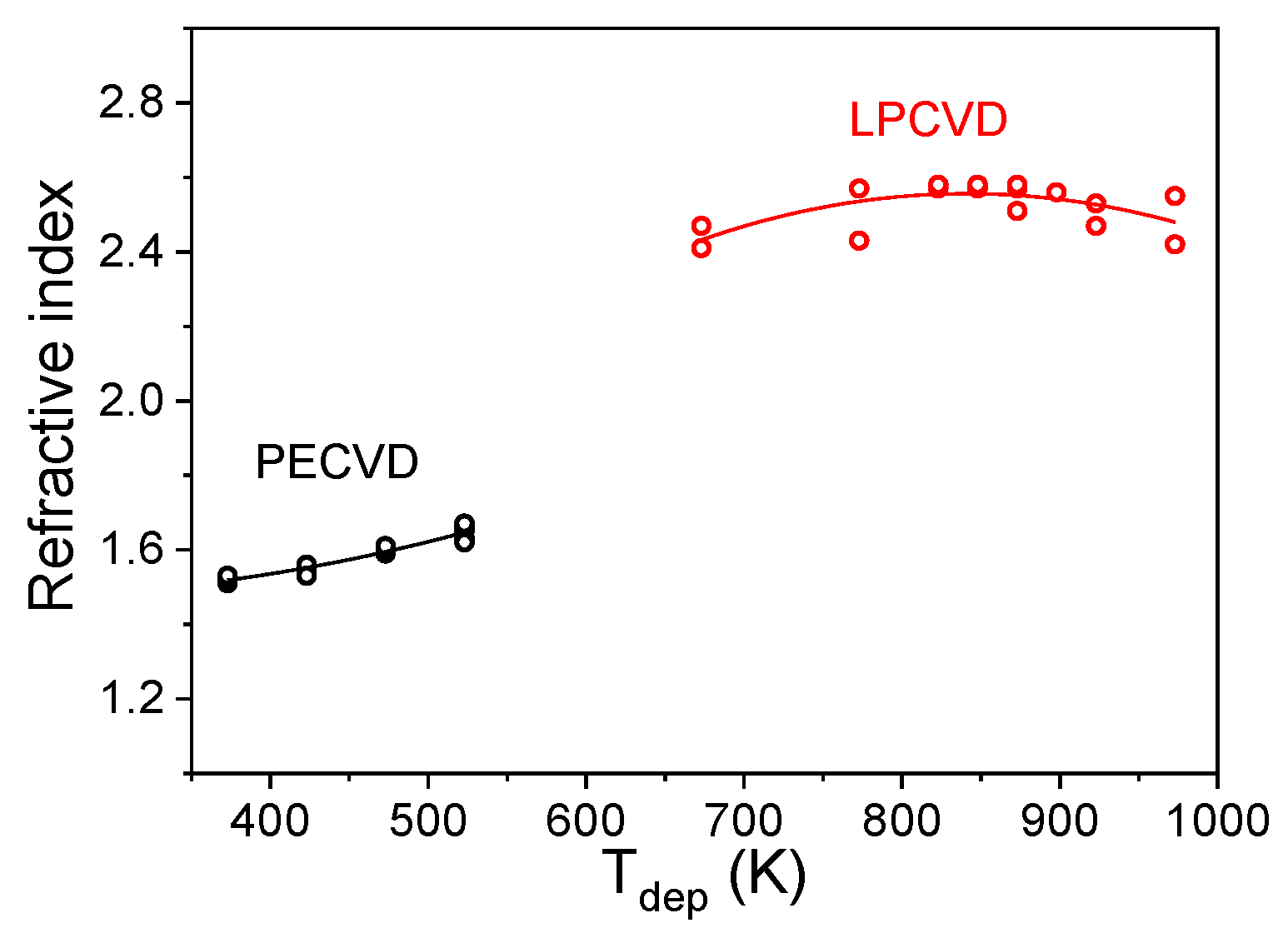
3.4.1. Optical Properties

Ellipsometry and spectrophotometry were used to study the optical properties of BCxNy films.
As known, the refractive index of h-BN and h-BCxNy is influenced by several factors, such as the composition of the films, their stoichiometry, the presence of hydrogen and oxygen-containing bonds, the chemical bond structure, stresses in the films, etc. The authors [89] reported that h-BN flakes of about 50 µm thickness had n|| = 2.14, n = 1.84. For h-BN films, the value of the refractive index, equal to 1.8, is given in the reference [90]. In [91] the refractive index of CVD BN films was measured as a function of the film composition. Its value ranged in the interval from 1.7 to 2.8 with an increase in the [B]:[N] ratio from 0.7 to 4, respectively. Thus, this indicates that the boron content in the film controls the refractive index, and boron-rich films have higher n values. In another study, a decrease in the refractive index of h-BN films with ratio [B]:[N] = 1:1, but having hydrogen-containing bonds and B–OH groups, is shown [92]. The presence of boron oxide in the films also contributes to a decrease in the value of n, since its refractive index is 1.45 (λ = 589 nm) [93]. Known from our previous investigation [31], the refractive index of BCxNy films deposited by the PECVD method using TMAB + NH3 mixture at substrate temperatures from 573 to 973 K changed from 1.56 to 2.27, respectively.
Figure 10 shows the dependences of the refractive index on the substrate temperature. The n values for LPCVD films change insignificantly with an increase in the synthesis temperature and lie in the range of 2.41–2.58. Such values are typical for BCxNy films with very low nitrogen content (Table 1) and BCx films [52].
Films obtained in the plasma-stimulated process have much lower values of refractive index. The values of n increase with increasing Tdep from 1.51 to 1.67. It can be seen that for each series, this value varies in a narrow range. A difference in the values of the refractive index for the studied LPCVD and PECVD films can be explained by a significant difference in their chemical composition with dominant bonds of B–C and B–N, B–C–N, respectively. According to data [58], with the deposition temperature increase from 373 to 973 K, n was between 1.52–1.65 for PECVD films obtained in a similar process using the mixture of N-trimethylborazine and N2. The refractive indexes equal to 1.58–1.65 were determined for films with a high content of B–N bonds obtained by LPCVD from a mixture of TMAB+NH3 at the high partial pressures of ammonia [36].
The optical properties of the BCxNy/SiO2 structures were studied with UV-Vis-NIR spectroscopy using a double-beam spectrophotometer. Figure 11a shows the transmittance spectra in the wavelength range of 190–2200 nm for the films of LPCVD and PECVD series and the spectrum of a fused silica substrate. The transparency of LPCVD films is 83–85% in the red and IR range. The PECVD process allows depositing films with transparency of 92–95% in the visible and IR regions of the spectrum. The absorption edge of PECVD films is shifted to the short-wave region compared to LPCVD films. Obviously, this difference is due to the predominance of B–N and B–C bonds in the films, respectively. In the work [54], a gradual increase in the transparency of BCxNy films and shifting of the absorption edge to the short-wave region with an increase in the nitrogen content in these films was demonstrated. On the other hand, the appearance of an additional phase of disordered amorphous carbon in the films leads to a decrease in their transparency [52,61].
The values of the optical band gap were estimated from Tauc’s plot [47]. With an increase in the film synthesis temperature, the band gap of LPCVD films varies in the ranges of 1.72–1.79 eV and 2.20–2.05 eV according to spectrophotometry and spectral ellipsometry, respectively (Figure 11b). The difference between the values obtained by the two optical methods is probably due to the effect of interference fringes on the results of calculations based on the transmission spectra. The PECVD films exhibit a slight decrease in the values of Eg from 5.28 to 4.92 eV with a rise in deposition temperature. This difference deals with variations in their chemical composition. The calculated values of band gaps are in good agreement with the reported values for BCx and BCxNy films. It is known from the literature that Eg values of BCx films deposited by magnetron sputtering of the B4C target lie in the interval of 1.1–2.8 eV [52]. The optical band gap of BCxNy films obtained by different CVD methods can vary over a wide range. With increasing deposition temperature from 373 to 973 K, Eg values decreased from 4.6 to 1.8 eV and from 4.9 to 1.2 for PECVD BCxNy films synthesized using mixtures of N-triethylborazine with NH3 and He, respectively [63]. On the other hand, the Eg value of the C-doped BN films decreased from 5.16 to 4.04 eV with increasing carbon content, since this contributed to the increase of π bonding originating from C=C bonds [94].

3.4.2. Wettability

The wetting behavior of the films’ surface was studied depending on the deposition parameters. The wettability of films was evaluated by measuring the contact angles (CA) of polar (water) and nonpolar (diethylene glycol, DEG) test liquids, followed by calculating the surface free energy. The contact angles of wetting were measured in the sessile drop mode. The profile of a sessile drop on a solid surface was created by numerically solving the Young-Laplace equation. The parameters derived from this theoretical droplet modeling method were compared with their respective counterparts from the ellipse fitting method. The results demonstrate that the ellipse fitting method is in excellent agreement with the Young-Laplace equation solution (Table 6). The repeatability of measurements is represented as errors in Table 6, which are less than 5%. It is known, the wetting behavior of a film’s surface is dependent on both surface topography and surface chemistry. As shown above, the low-temperature PECVD and all LPCVD films have very low roughness.
The angle values given in Table 6 indicate the moderate hydrophilicity of all deposited films. The water contact angles lie in the region from 59 ± 3° to 63 ± 2° for LPCVD BCx-like films deposited at temperatures from 773 to 898 K, respectively. The contact angle is reduced to 53° for films produced at higher temperatures. It should be noted that, according to the Raman spectroscopy data, these films contain an impurity phase of amorphous graphite-like carbon. According to the results of the XPS data, the top layer of LPCVD films contains about 11–12 at.% oxygen. As is known, oxygen-containing groups can contribute to a decrease in the contact angles. The obtained values of the water contact angles are consistent with the literature data for BCxNy films deposited by magnetron sputtering where CA = 50–77° [95] and 20.7–54.0° [96].
PECVD BCxNyOz films’ wettability experiments showed that the films obtained at 373–423 K degraded upon interaction with the test liquid. Films synthesized at a higher temperature exhibited hydrophilic behavior (Table 6). The hydrophilicity of these films may be associated with the presence of NH and oxygen-containing surface functional groups.

3.4.3. Mechanical Properties

The values of hardness and Young’s modulus for LPCVD films obtained in the temperature range of 773–923 K do not change (Figure 12, Table 7) and slightly decrease when the temperature reaches 973 K. As seen from XPS data (Figure 8), these films are BCx-like materials with high content of B–C bonds and very low nitrogen content. A decrease in hardness may be due to the appearance of an additional carbon phase, as can be seen from the Raman spectra. According to [97], the H and E of crystalline B4C are 25–40 GPa and 441–472 GPa, respectively. The hardness of LPCVD BCxNy films deposited using mixtures of TMAB + He and TMAB + NH3 was 34 and 10–15 GPa, respectively [34]. The hardness of films, obtained in the same processes with the use of (C2H5)3N·BH3 +N2+NH3 [60] and B3N3H3(CH3)3 + C6H5CH3 + NH3 + N2, was 12 and 20 GPa, respectively [98].
The elasticity index (H/E) is used to determine the elastic limit for surface contact [99]. The plasticity index (H3/E2) describes the material resistance to plastic deformation [100] and the fracture toughness of a thin solid film [99]. Therefore, these parameters are important for preventing wear. The coating with optimized H, H/E, and H3/E2 values is expected to exhibit exceptional wear resistance. Figure 12b presents the temperature dependencies of elasticity and plasticity indexes of the LPCVD BCxNy films.
The scratch adhesion test was employed to evaluate the degree of adherence between the BCxNy film and Si(100) substrate. The topology of scratch tracks was studied via an AFM mode of NanoScan-3D scanning nanohardness tester immediately after the scratching. It was observed that scratching the LPCVD samples (Figure 13) led to the formation of local fractures around the scratch’s periphery at certain critical loads during the pyramidal tip test: Lc1 for the edge-forward orientation and Lc2 for the face-forward orientation. According to [101], different attack angles correspond to different deformation modes: the face-forward orientation is close to microcutting while the edge-forward orientation is closer to plastic extrusion. No significant exfoliation of the films from the substrates was observed. For films deposited at temperatures of 773–923 K, the values of Lc1 are 28–32 mN, and Lc2 are 21–26 mN (Figure 13f). For high-temperature film (Tdep = 973 K), the values of Lc1 and Lc2 increase to 49 and 42 mN, respectively. It should be emphasized that among the studied films, these films have the highest adhesion to the Si(100) substrate. For comparison, consider the literature data obtained by scratch-test with the Berkovich indenter. The magnetron sputtered BCxNy films had values of Lc2 equal to 18–30 mN depending on the films’ composition [102]. In another study, the values of Lc1 = 32 mN and Lc2 = 25 mN were obtained for the magnetron sputtered BCx-like film; and critical loads for BCxNy films led in the intervals of Lc1 = 12–57 mN and Lc2 = 8–41 mN [96].
The values of H and E of PECVD films deposited at Tdep = 373–523 K are significantly smaller than for LPCVD films and equal to 0.76–1.40 GPa and 25–26 GPa, respectively (Figure 14 and Table 8). It should be emphasized that these hardness values are higher than that of polycrystalline h-BN powder (H = 0.05–0.6 GPa) [103]. A significant decrease in the values of H and E compared to LPCVD films is associated with the dominance of “softer” sp2 B–N and sp2 B–C–N bonds and a smaller number of B–C bonds [3,104,105]. The presence of hydrogen- and oxygen-containing bonds also contributed to the decrease in values of mechanical performances [52]. The elasticity and plasticity indexes (Figure 14b) and recovery (Table 8) are also significantly lower than those of LPCVD films.
The adhesion of the PECVD BCxNyOz films to the Si(100) substrate was evaluated by a scratch test under the same conditions as for LPCVD films (Figure 15). It should be noted that due to the low mechanical properties of these films, the indenter reaches the substrate almost at the beginning of the scratch under loads Lc1 and Lc2. Wherein scratching PECVD films, at both angles of penetration of the indenter (edge- and face-forward), no delamination of the film material is observed, but only its extrusion occurs. Such a reaction to the penetration of an indenter is characteristic of soft films, which are the studied PECVD samples. Based on the scratch behavior of the PECVD coating, it can be assumed that the interfacial shear stress with the silicon substrate is less than the shear strength of the film itself as a softer component.

4. Conclusions

For experimental realization, we synthesized amorphous BCxNy films by decomposition of the mixture of trimethylamine borane and nitrogen (PTMAB:PN2 = 1:1) using both LPCVD and PECVD processes at 673–973 K and 373–523 K, respectively. Various processing temperatures were used to study the effect of temperature on BCxNy films’ properties. It should be emphasized that the type of activation of the gas phase (thermal or plasma) has a significant effect on the composition of the synthesized films. The composition of films deposited by the LPCVD method close to BCx with very low nitrogen concentration. In contrast to the LPCVD films where B–C bonds were dominant, the PECVD films have BCxNyOz:H composition and a complex chemical structure. The broad bands of the XPS spectra suggest that the films are composed of different B–N and B–C–N bonds in forming the sp2 B–C–N atomic hybrid configuration. Thus, the deposition technique offers the ability to control the films’ properties.
The films deposited by LPCVD exhibit the highest hardness, about 28 GPa, and the highest elastic modulus, about 243 GPa. This fact could be explained by the high amount of B–C bonds. The increase in the nitrogen content in the films, which was achieved using the PECVD method, dropped sharply the values of mechanical properties.
The highly transparent films with a transmittance of up to 95% were obtained only in the PECVD process. The values of the refractive index and optical band gap are also sensitive to the preparation method of the films. The LPCVD films had higher refractive indexes and lower optical bandgaps.
According to our experimental results of the decomposition of the TMAB + N2 mixture, we can recommend the use of the LPCVD method to obtain the hard hydrophilic BCxNy films and the PECVD method for the deposition of the transparent hydrophilic BCxNyOz:H films.

Supplementary Materials

The following supporting information can be downloaded at: https://www.mdpi.com/article/10.3390/app13084959/s1, Figure S1: Dependence of (a) hardness and (b) Young’s modulus on the indentation depth for the LPCVD BCxNy film (Tdep = 773 K); Figure S2: XRD patterns of Si(100) substrate and BCxNy films deposited by LPCVD and PECVD processes at 973 and 523 K, respectively.

Author Contributions

Conceptualization, S.V.B. and M.L.K.; methodology, S.V.B. and M.L.K.; validation, S.V.B.; formal analysis, E.A.M., V.R.S., A.A.S. (Aleksandra A. Shapovalova), A.N.K., A.A.S. (Andrey A. Saraev), I.P.A., M.N.K., I.V.Y. and A.G.P.; investigation, E.A.M., V.R.S., A.N.K., A.A.S. (Andrey A. Saraev), I.P.A. and I.V.Y.; writing—original draft preparation, S.V.B.; writing—review and editing, V.S.S. and M.L.K.; visualization, S.V.B., E.A.M., A.N.K., A.A.S. (Andrey A. Saraev), I.P.A., M.N.K. and I.V.Y.; supervision, M.L.K.; project administration, M.L.K.; funding acquisition, M.L.K. All authors contributed to the discussion and interpretation of the results. All authors have read and agreed to the published version of the manuscript.

Funding

The research was supported by the Ministry of Science and Higher Education of the Russian Federation, project N 121031700314-5.

Institutional Review Board Statement

Not applicable.

Informed Consent Statement

Not applicable.

Data Availability Statement

Not applicable.

Acknowledgments

The authors thank B.A. Kolesov for the Raman spectroscopy study, I.V. Korolkov for the XRD study, and A.K. Kozhevnikov for visualization of a part of data.

Conflicts of Interest

The authors declare no conflict of interest.

References

  1. Skakalova, V.; Kaiser, A. (Eds.) Graphene: Properties, Preparation, Characterization and Applications, 2nd ed.; Woodhead Publishing: Philadelphia, PA, USA, 2021; p. 544. [Google Scholar]
  2. Hayat, A.; Sohail, M.; Hamdy, M.S.; Taha, T.A.; AlSalem, H.S.; Alenad, A.M.; Amin, M.A.; Shah, R.; Palamanit, A.; Khan, J.; et al. Fabrication, characteristics, and applications of boron nitride and their composite nanomaterials. Surf. Interfaces 2022, 29, 101725. [Google Scholar] [CrossRef]
  3. Nehate, S.D.; Saikumar, A.K.; Prakash, A.; Sundaram, K.B. A review of boron carbon nitride thin films and progress in nanomaterials. Mater. Today Adv. 2020, 8, 100106. [Google Scholar] [CrossRef]
  4. Yu, L.A.; Chebanova, G.E.; Artemkina, S.B.; Lavrov, A.N. Crystalline and nanostructured materials based on transition metal dichalcogenides: Synthesis and electronic properties. J. Struct. Chem. 2022, 63, 176–226. [Google Scholar]
  5. He, Z.; Zhang, S.; Zheng, L.; Liu, Z.; Zhang, G.; Wu, H.; Wang, B.; Liu, Z.; Jin, Z.; Wang, G. Si-Based NIR Tunneling Heterojunction Photodetector with Interfacial Engineering and 3D-Graphene Integration. IEEE Electron Device Lett. 2022, 43, 1818–1821. [Google Scholar] [CrossRef]
  6. Yu, L.; Zhang, S.; Zhang, G.; He, Z.; Feng, X.; Liu, Z.; Wang, G.; Tao, W.; Zheng, L.; Yang, S.; et al. Dual-Enhanced Photodetectors Combining Graphene Plasmonic Nanoresonators With Germanium-on-Insulator Optical Cavities. IEEE Trans. Electron Devices 2022, 69, 3246–3250. [Google Scholar] [CrossRef]
  7. Zheng, L.; Zhou, W.; Ning, Z.; Wang, G.; Cheng, X.; Hu, W.; Zhou, W.; Liu, Z.; Yang, S.; Xu, K.; et al. Ambipolar Graphene–Quantum Dot Phototransistors with CMOS Compatibility. Adv. Opt. Mater. 2018, 6, 1800985. [Google Scholar] [CrossRef]
  8. Pristáš, G.; Werheit, H.; Gabáni, S.; Shalamberidze, S.; Flachbart, K. Low Temperature Specific Heat Anomaly with Boson Peak in Isotope-Enriched Boron Carbides B4.3C–B10C. Solid State Sci. 2020, 101, 106140. [Google Scholar] [CrossRef]
  9. Suri, A.K.; Subramanian, C.; Sonber, J.K.; Murthy, T.S.R.C. Synthesis and Consolidation of Boron Carbide: A Review. Int. Mater. Rev. 2010, 55, 4–40. [Google Scholar] [CrossRef]
  10. Beauvy, M. Stoichiometric Limits of Carbon-Rich Boron Carbide Phases. J. Less-Common Met. 1983, 90, 169–175. [Google Scholar] [CrossRef]
  11. Werheit, H.; Shalamberidze, S. Advanced Microstructure of Boron Carbide. J. Phys. Condens. Matter 2012, 24, 385406. [Google Scholar] [CrossRef]
  12. Miele, P.; Bechelany, M. (Eds.) Boron Nitride Nanostructures; MDPI: Basel, Switzerland, 2018; p. 104. [Google Scholar]
  13. Gonzalez-Ortiz, D.; Salameh, C.; Bechelany, M.; Miele, P. Nanostructured boron nitride-based materials: Synthesis and applications. Mater. Today Adv. 2020, 8, 100107. [Google Scholar] [CrossRef]
  14. Uddin, M.R.; Majety, S.; Li, J.; Lin, J.Y.; Jiang, H.X. Layer-structured hexagonal (BN)C semiconductor alloys with tunable optical and electrical properties. J. Appl. Phys. 2014, 115, 093509. [Google Scholar] [CrossRef] [Green Version]
  15. Mannan, M.A.; Noguchi, H.; Kida, T.; Nagano, M.; Hirao, N.; Baba, Y. Growth and characterization of stoichiometric BCN films on highly oriented pyrolytic graphite by radiofrequency plasma enhanced chemical vapor deposition. Thin Solid Film. 2010, 518, 4163–4169. [Google Scholar] [CrossRef]
  16. Hoffmann, P.; Fainer, N.; Kosinova, M.; Baake, O.; Ensinger, W. Chapter 21. Compilation on Synthesis, Characterization and Properties of Silicon and Boron Carbonitride Films. In Silicon Carbide—Materials, Processing and Applications in Electronic Devices; Mukherjee, M., Ed.; InTech: Rijeka, Croatia, 2011; pp. 487–546. [Google Scholar]
  17. Husain, E.; Narayanan, T.N.; Taha-Tijerina, J.J.; Vinod, S.; Vajtai, R.; Ajayan, P.M. Marine Corrosion Protective Coatings of Hexagonal Boron Nitride Thin Films on Stainless Steel. ACS Appl. Mater. Interfaces 2013, 5, 4129–4135. [Google Scholar] [CrossRef] [PubMed]
  18. Fan, Y.; Yang, H.; Fan, H.; Liu, Q.; Lv, C.; Zhao, X.; Yang, M.; Wu, J.; Cao, X. Corrosion resistance of modified hexagonal boron nitride (h-BN) nanosheets doped acrylic acid coating on hot-dip galvanized steel. Materials 2020, 13, 2340. [Google Scholar] [CrossRef]
  19. Dong, P.V.; Phan, N.H.; Patil, S.; Shirguppikar, S.; Kalel, S.; Thanh, L.T.P.; Hien, D.M. Effect of boron carbide reinforcement on properties of stainless-steel metal matrix composite for nuclear applications. J. Mech. Behav. Mater. 2022, 31, 390–397. [Google Scholar] [CrossRef]
  20. Kharanzhevsky, E.V.; Reshetnikov, S.M.; Efimov, A.V.; Gil’mutdinov, F.Z.; Krivilev, M.D. Application of some inhibitors for improving the corrosion resistance of ceramic coatings deposited on non-alloy steel by short-pulse laser treatment. Int. J. Corros. Scale Inhib. 2020, 9, 44–55. [Google Scholar]
  21. Shayapov, V.R.; Zakharchenko, K.V.; Kapustin, V.I.; Merenkov, I.S.; Khomyakov, M.N.; Maksimivskiy, E.A. Hardness and Strengthening Effect of Low-Pressure Chemical Vapor Deposition BCxNy Coatings Deposited on Ti-6Al-4V Alloy. J. Mater. Eng. Perform. 2022, 31, 3792–3798. [Google Scholar] [CrossRef]
  22. Duan, C.; Li, X.; Ji, Y.; He, L.; Qian, J.; Zhao, Z. In-Situ Catalytic Preparation of Two-Dimensional BCN/Graphene Composite for Anti-Corrosion Application. Catalysts 2022, 12, 1618. [Google Scholar] [CrossRef]
  23. Oliveira, M.N.; Conde, O. Synthesis and properties of BxCyNz coatings. J. Mater. Res. 2001, 16, 734–743. [Google Scholar] [CrossRef]
  24. Yamada, M.; Nakaishi, M.; Sugishima, K. Improvements of stress controllability and radiation resistance by adding carbon to boron-nitride. J. Elecrochem. Soc. 1990, 137, 2242–2246. [Google Scholar] [CrossRef]
  25. Yasui, H.; Awazu, K.; Ikenaga, N.; Sakudo, N. Synthesis and characterization of BN thin films prepared by plasma MOCVD with organoboron precursors. Vacuum 2009, 83, 582–584. [Google Scholar] [CrossRef]
  26. Kesler, V.G.; Kosinova, M.L.; Rumyantsev, Y.M.; Sulyaeva, V.S. X-ray photoelectron and auger spectroscopic study of the chemical composition of BCxNy films. J. Struct. Chem. 2012, 53, 699–707. [Google Scholar] [CrossRef]
  27. Baake, O.; Hoffmann, P.S.; Kosinova, M.L.; Klein, A.; Pollakowski, B.; Beckhoff, B.; Fainer, N.I.; Trunova, V.A.; Ensinger, W. Analytical characterization of BCxNy films generated by LPCVD with triethylamine borane. Anal. Bioanal. Chem. 2010, 398, 1077–1084. [Google Scholar] [CrossRef]
  28. Mannan, M.A.; Baba, Y.; Hirao, N.; Kida, T.; Nagano, M.; Noguchi, H. Hexagonal Nano-Crystalline BCN Films Grown on Si (100) Substrate Studied by X-Ray Absorption Spectroscopy. Mater. Sci. Appl. 2013, 4, 11–19. [Google Scholar] [CrossRef] [Green Version]
  29. Leardini, F.; Jiménez-Arévalo, N.; Jimenez-Ferrer, I.; Ares, J.-R.; Molina, P.; Gomez-Navarro, C.; Manzanares, Y.; Granados, D.; Urbanos, F.J.; Garcia-Garcia, J.; et al. A fast synthesis route of Boron-Carbon-Nitrogen ultrathin layers towards highly mixed ternary B-C-N phases. 2D Mater. 2019, 6, 035015. [Google Scholar] [CrossRef]
  30. Nappini, S.; Bondino, F.; Píš, I.; Chelleri, R.; Greco, S.L.; Lazzarino, M.; Magnano, E. Chemical composition and interaction strength of two-dimensional boron-nitrogen-carbon heterostructures driven by polycrystalline metallic surfaces. Appl. Surf. Sci. 2019, 479, 903–913. [Google Scholar] [CrossRef]
  31. Kosinova, M.L.; Rumyantsev, Y.M.; Golubenko, A.N.; Fainer, N.I.; Ayupov, B.M.; Dolgovesova, I.P.; Kolesov, B.A.; Kaichev, V.V.; Kuznetsov, F.A. Chemical Composition of Boron Carbonitride Films Grown by Plasma-Enhanced Chemical Vapor Deposition from Trimethylamineborane. Inorg. Mater. 2003, 39, 366–373. [Google Scholar] [CrossRef]
  32. Burg, A.B.; Schlesin, H.I. Hydrides of Boron. VII. Evidence of the Transitory Existence of Borine (BH3): Borine Carbonyl and Borine Trimethylammine. J. Am. Chem. Soc. 1937, 59, 780–786. [Google Scholar] [CrossRef]
  33. Alton, E.R.; Brown, R.D.; Carter, J.C.; Taylor, R.C. Vapor Pressures of the Methylamine-Boranes and Ammonia-Triborane. J. Am. Chem. Soc. 1959, 81, 3550–3551. [Google Scholar] [CrossRef]
  34. Kosinova, M.L.; Fainer, N.I.; Sulayeva, V.S.; Rumyantsev, Y.M.; Kuznetsov, F.A.; Maximovski, E.A.; Cao, Z.X.; Terauchi, M.; Shibata, K.; Satoh, F. Synthesis, nanoindentation and AFM studies of CVD boron carbon nitride films. ECS Proc. EUROCVD-15 2005, 2005-09, 1082–1087. [Google Scholar]
  35. Hoffmann, P.; Baake, O.; Beckhoff, B.; Ensinger, W.; Fainer, N.; Klein, A.; Kosinova, M.; Pollakowski, B.; Trunova, V.; Ulm, G.; et al. Chemical bonding in carbonitride nanolayers. Nucl. Instrum. Methods Phys. Res. A 2007, 575, 78–84. [Google Scholar] [CrossRef]
  36. Baake, O.; Hoffmann, P.S.; Klein, A.; Pollakowski, B.; Beckhoff, B.; Ensinger, W.; Kosinova, M.; Fainer, N.; Sulyaeva, V.S.; Trunova, V. Chemical character of BCxNy layers grown by CVD with trimethylamine borane. X-Ray Spectrom. 2009, 38, 68–73. [Google Scholar] [CrossRef]
  37. Sulyaeva, V.S.; Kesler, V.G.; Kosinova, M.L. Dielectric layers BCxNy: Synthesis by the decomposition of vapors of organoboron compounds, composition and chemical structure. J. Struct. Chem. 2021, 62, 1631–1647. [Google Scholar] [CrossRef]
  38. Kosinova, M.L.; Rumyantsev, Y.M.; Fainer, N.I.; Maximovskii, E.A.; Kuznetsov, F.A. The structure study of boron carbonitride films obtained by use of trimethylaminoborane complex. Nucl. Instrum. Methods Phys. Res. A 2001, 470, 253–257. [Google Scholar] [CrossRef]
  39. Kosinova, M.L.; Fainer, N.I.; Rumyantsev, Y.M.; Maximovski, E.A.; Kuznetsov, F.A.; Terauchi, M.; Shibata, K.; Satoh, F. Growth of homogeneous and gradient BCxNy films by PECVD using trimethylamino borane complex. In Proceedings of Chemical Vapor Deposition XVI and EUROCVD 14: Proceedings of the International Symposium, Paris, France, 27 April–2 May 2003; Electrochemical Society: Pennington, NJ, USA, 2003; Volume 2003-08, pp. 708–715. [Google Scholar]
  40. Mannan, M.A.; Nagano, M.; Shigezumi, K.; Kida, T.; Hirao, N.; Baba, Y. Characterization of Boron Carbonitride (BCN) Thin Films Deposited by Radiofrequency and Microwave Plasma Enhanced Chemical Vapor Deposition. Am. J. Appl. Sci. 2007, 5, 736–741. [Google Scholar] [CrossRef] [Green Version]
  41. Kida, T.; Shigezumi, K.; Mannan, M.A.; Akiyama, M.; Baba, Y.; Nagano, M. Synthesis of boron carbonitride (BCN) films by plasma-enhanced chemical vapor deposition using trimethylamine borane as a molecular precursor. Vacuum 2009, 83, 1143–1146. [Google Scholar] [CrossRef]
  42. Smith, D.L. Mechanism of SiNxHy deposition from N2–SiH4 plasma. J. Vac. Sci. Technol. B 1990, 8, 551–557. [Google Scholar] [CrossRef]
  43. Alexandrov, S.E.; Hitchman, M.L. Chapter12 Plasma Enhanced Chemical Vapour Deposition Processes. In Chemical Vapour Deposition: Precursors, Processes and Applications; Jones, A.C., Hitchman, M.L., Eds.; Royal Society of Chemistry: London, UK, 2009; pp. 494–509. [Google Scholar]
  44. Kosinova, M.L.; Fainer, N.I.; Rumyantsev, Y.M.; Golubenko, A.N.; Kuznetsov, F.A. LPCVD Boron Carbonitride Films From Trimethylamine Borane. J. Phys. 1999, 4, Pr. 8-915–Pr. 8-921. [Google Scholar]
  45. Sulyaeva, V.S.; Plekhanov, A.G.; Maksimovskii, E.A.; Fainer, N.I.; Rumyantsev, Y.M.; Kosinova, M.L. Characterization of Thin Boron and Silicon Carbonitride Films by Wavelength Dispersive Spectroscopy. Prot. Met. Phys. Chem. Surf. 2017, 53, 1187–1191. [Google Scholar] [CrossRef]
  46. Forouhi, A.R.; Bloomer, I. Optical dispersion relations for amorphous semi-conductors and amorphous dielectrics. Phys. Rev. B. 1986, 34, 7018–7026. [Google Scholar] [CrossRef] [PubMed]
  47. Tauc, J.; Menth, A. States in the gap. J. Non-Cryst. Solids 1972, 8, 569–585. [Google Scholar] [CrossRef]
  48. Scofield, J.H. Hartree-Slater subshell photoionization cross-sections at 1254 and 1487 eV. J. Electron Spectrosc. Relat. Phenom. 1976, 8, 129–137. [Google Scholar] [CrossRef]
  49. Tanuma, S.; Powell, C.J.; Penn, D.R. Calculations of electron inelastic mean free paths. V. Data for 14 organic compounds over the 50–2000 eV range. Surf. Interf. Anal. 1994, 21, 165–176. [Google Scholar] [CrossRef]
  50. Kwok, D.Y.; Neumann, A.W. Contact angle measurements and contact angle interpretation. Adv. Colloid Interface Sci. 1999, 81, 167–249. [Google Scholar] [CrossRef]
  51. Owens, D.K.; Wendt, R.C. Estimation of the surface free energy of polymers. J. Appl. Polym. Sci. 1969, 13, 1741–1747. [Google Scholar] [CrossRef]
  52. Sulyaeva, V.; Khomyakov, M.; Kosinova, M. Room-Temperature Formation of Hard BCx Films by Low Power Magnetron Sputtering. Appl. Sci. 2021, 11, 9896. [Google Scholar] [CrossRef]
  53. Korsunsky, A.M.; McGurk, M.R.; Bull, S.J.; Page, T.F. On the hardness of coated systems. Surf. Coat. Technol. 1998, 99, 171–183. [Google Scholar] [CrossRef]
  54. Hoffmann, P.S.; Baake, O.; Kosinova, M.L.; Beckhoff, B.; Klein, A.; Pollakowski, B.; Trunova, V.A.; Sulyaeva, V.S.; Kuznetsov, F.A.; Ensinger, W. Chemical bonds and elemental compositions of BCxNy layers produced by chemical vapor deposition with trimethylamine borane, triethylamine borane, or trimethylborazine. X-Ray Spectrom. 2012, 41, 240–246. [Google Scholar] [CrossRef]
  55. Engbrecht, E.R.; Cilino, C.J.; Junker, K.H.; Sun, Y.-M.; White, J.M.; Ekerdt, J.G. Charac-terization of Boron Carbo-Nitride Films Deposited By Low Temperature Chemical Vapor Deposition. Mat. Res. Soc. Symp. Proc. 2003, 766, E8.21.1–E8.21.6. [Google Scholar] [CrossRef]
  56. Bath, A.; van der Put, P.J.; Lepley, B. Study of boron nitride gate insulators grown by low temperature plasma enhanced chemical vapor deposition on InP. Appl. Surf. Sci. 1989, 39, 135–140. [Google Scholar] [CrossRef] [Green Version]
  57. Hiramatsu, M.; Hori, M. Carbon Nanowalls. Synthesis and Emerging Applications; Springer: Wien, Austria, 2010; p. 161. [Google Scholar]
  58. Sulyaeva, V.; Kosinova, M.; Rumyantsev, Y.; Golubenko, A.; Fainer, N.; Alferova, N.; Ayupov, B.M.; Gevko, P.N.; Kesler, V.G.; Kolesov, B.A.; et al. Properties of BC x N y films grown by plasma-enhanced chemical vapor deposition from N-trimethylborazine-nitrogen mixtures. Inorg. Mater. 2010, 46, 487–494. [Google Scholar] [CrossRef]
  59. Zaumseil, P. High-resolution characterization of the forbidden Si 200 and Si 222 reflections. J. Appl. Cryst. 2015, 48, 528–532. [Google Scholar] [CrossRef] [Green Version]
  60. Levy, R.A.; Mastromatteo, E.; Grow, J.M.; Paturi, V.; Kuo, W.P. Low pressure chemical vapor deposition of B-N-C-H films from triethylamine borane complex. J. Mater. Res. 1995, 10, 320–327. [Google Scholar] [CrossRef]
  61. Sulyaeva, V.S.; Rumyantsev, Y.M.; Kesler, V.G.; Kosinova, M.L. Synthesis and optical properties of BCxNy films deposited from N-triethylborazine and hydrogen mixture. Thin Solid Film. 2015, 581, 59–64. [Google Scholar] [CrossRef]
  62. Merenkov, I.S.; Kasatkin, I.A.; Maksimovskii, E.A.; Alferova, N.I.; Kosinova, M.L. Vertically aligned layers of hexagonal boron nitride: PECVD synthesis from triethylaminoborane and structural features. J. Struct. Chem. 2017, 58, 1018–1024. [Google Scholar] [CrossRef]
  63. Sulyaeva, V.S.; Kosinova, M.L.; Rumyantsev, Y.M.; Kesler, V.G.; Kuznetsov, F.A. PECVD synthesis and optical properties of BCxNy films obtained from N-triethylborazine as a single-source precursor. Surf. Coat. Technol. 2013, 230, 145–151. [Google Scholar] [CrossRef]
  64. Sulyaeva, V.S.; Kosinova, M.L.; Rumyantsev, Y.M.; Kuznetsov, F.A.; Kesler, V.G.; Kirienko, V.V. Optical and electrical characteristics of plasma-enhanced chemical vapor deposition boron carbonitride thin films derived from N-trimethylborazine precursor. Thin Solid Film. 2014, 558, 112–117. [Google Scholar] [CrossRef]
  65. Binnenbruck, H.; Werheit, H. IR-Active Phonons of Boron and Boron Carbide. J. Phys. Sci. 1979, 34, 787–798. [Google Scholar] [CrossRef]
  66. Werheit, H.; Manghnani, M.H.; Kuhlmann, U.; Hushur, A.; Shalamberidze, S. Mode Grüneisen parameters of boron carbide. Sol. State Sci. 2017, 72, 80–93. [Google Scholar] [CrossRef]
  67. Shirai, K.; Emura, S.; Gonda, S.I. Infrared study of amorphous B1-xCx, films. J. Appl. Phys. 1995, 78, 3392–3400. [Google Scholar] [CrossRef]
  68. Geick, R.; Perry, C.H.; Rupprecht, N.G. Modes in Hexagonal Boron Nitride. Phys. Rev. 1966, 146, 543–547. [Google Scholar] [CrossRef]
  69. Demin, V.N.; Asanov, I.P.; Akkerman, Z.L. Chemical vapor deposition of pyrolytic boron nitride from borazine. J. Vac. Sci. Technol. A 2000, 18, 94–98. [Google Scholar] [CrossRef]
  70. Bellamy, L.J. The Infrared Spectra of Complex Molecules, 3rd ed.; Springer: Berlin, Heidelberg, Germany, 1975; p. 433. [Google Scholar]
  71. Weltner, W.; Warn, J.R.W. Matrix Isolation of High-Temperature Vapors: Boric Oxide. J. Chem. Phys. 1962, 37, 292–303. [Google Scholar] [CrossRef]
  72. Putkonen, M.; Niinistö, L. Atomic layer deposition of B2O3 thin films at room temperature. Thin Solid Film. 2006, 514, 145–149. [Google Scholar] [CrossRef]
  73. Parker, J.H.; Feldman, D.W.; Ashkin, M. Raman scattering by silicon and germanium. Phys. Rev. 1967, 155, 712–714. [Google Scholar] [CrossRef]
  74. Tallant, D.R.; Aselage, T.L.; Campbell, A.N.; Emin, D. Boron carbide structure by Raman spectroscopy. Phys. Rev. B 1989, 40, 5649–5656. [Google Scholar] [CrossRef]
  75. Imam, M.; Höglund, C.; Jensen, J.; Schmidt, S.; Ivanov, I.G.; Hall-Wilton, R.; Birch, J.; Pedersen, H. Trimethylboron as Single-Source Precursor for Boron-Carbon Thin Film Synthesis by Plasma Chemical Vapor Deposition. J. Phys. Chem. C 2016, 120, 21990–21997. [Google Scholar] [CrossRef] [Green Version]
  76. Walrafen, G.E.; Samanta, S.R.; Krishnan, P.N. Raman investigation of vitreous and molten boric oxid. J. Chem. Phys. 1980, 72, 113–120. [Google Scholar] [CrossRef]
  77. Parsons, J.L.; Milberg, M.E. Vibrational Spectra of Vitreous B2O3·xH2O. J. Amer. Ceram. Soc. 1960, 43, 326–330. [Google Scholar] [CrossRef]
  78. Wang, C.B.; Xiao, J.L.; Shen, Q.; Zhang, L.M. Bonding structure and mechanical properties of B-C-N thin films synthesized by pulsed laser deposition at different laser fluences. Thin Solid Film. 2016, 603, 323–327. [Google Scholar] [CrossRef]
  79. Puyoo, G.; Teyssandier, F.; Pailler, R.; Labrugère, C.; Chollon, G. Boron carbonitride coatings synthesized by LPCVD, structure and properties. Carbon 2017, 122, 19–46. [Google Scholar] [CrossRef] [Green Version]
  80. Prakash, A.; Sundaram, K.B. Optical and XPS studies of BCN thin films by co-sputtering of B4C and BN targets. Appl. Surf. Sci. 2017, 396, 484–491. [Google Scholar] [CrossRef]
  81. Briggs, D.; Seah, M.P. (Eds.) . Practical Surface Analysis. V.1.—Auger and X-ray Photoelectron Spectroscopy, 2nd ed.; John Wiley & Sons: Chichester, UK, 1995. [Google Scholar]
  82. Naumkin, A.V.; Kraut-Vass, A.; Gaarenstroom, S.W.; Powell, C.J. NIST X-ray Photoelectron Spectroscopy Databas. In NIST Standard Reference Database 20, Version 4.1; National Institute of Standards and Technology: Gaithersburg, MD, USA, 2012. [Google Scholar] [CrossRef]
  83. Ramana, C.V.; Vemuri, R.S.; Kaichev, V.V.; Kochubey, V.A.; Saraev, A.A.; Atuchin, V.V. X-ray Photoelectron Spectroscopy Depth Profiling of La2O3/Si Thin Films Deposited by Reactive Magnetron Sputtering. ACS Appl. Mater. Interfaces 2011, 3, 4370–4373. [Google Scholar] [CrossRef]
  84. Kim, D.H.; Byon, E.; Lee, S.; Kim, J.-K.; Ruh, H. Characterization of ternary boron carbon nitride films synthesized by RF magnetron sputtering. Thin Solid Film. 2004, 447–448, 192. [Google Scholar] [CrossRef]
  85. Uddin, M.N.; Shimoyama, I.; Baba, Y.; Sekiguchi, T.; Nagano, M. X-ray photoelectron spectroscopic observation on B–C–N hybrids synthesized by ion beam deposition of borazine. J. Vac. Sci. Technol. A Vac. Surf. Film. 2005, 23, 497–502. [Google Scholar] [CrossRef]
  86. Yan, X.; Xu, T.; Chen, G.; Yang, S.; Liu, H.; Xue, Q. Preparation and characterization of electrochemically deposited carbon nitride films on silicon substrate. J. Phys. D Appl. Phys. 2004, 37, 907. [Google Scholar] [CrossRef]
  87. Souqui, L.; Palisaitis, J.; Högberg, H.; Pedersen, H. Plasma CVD of B-C-N thin films using triethylboron in argon-nitrogen plasma. J. Mater. Chem. C 2020, 8, 4112–4123. [Google Scholar] [CrossRef] [Green Version]
  88. Chen, C.M.; Huang, J.Q.; Zhang, Q.; Gong, W.Z.; Yang, Q.H.; Wang, M.Z.; Yang, Y.G. Annealing a graphene oxide film to produce a free standing high conductive graphene film. Carbon 2012, 50, 659–667. [Google Scholar] [CrossRef]
  89. Rah, Y.; Jin, Y.; Kim, S.; Yu, K. Optical analysis of the refractive index and birefringence of hexagonal boron nitride from the visible to near-infrared. Opt. Lett. 2019, 44, 3797–3800. [Google Scholar] [CrossRef]
  90. Rumyantsev, S.L.; Levinshtein, M.E.; Jackson, A.D.; Mohammmad, S.N.; Harris, G.L.; Spencer, M.G.; Shur, M.S. Boron nitride (BN). In Properties of Advanced Semiconductor Materials GaN, AlN, InN, BN, SiC, SiGe; Levinshtein, M.E., Rumyantsev, S.L., Shur, M.S., Eds.; John Wiley & Sons, Inc.: New York, NY, USA, 2001; pp. 67–92. [Google Scholar]
  91. Murarka, S.P.; Chang, C.C.; Wang, D.N.K.; Smit, T.E. Effect of Growth Parameters on the CVD of Boron Nitride and Phosphorus-Doped Boron Nitride. J. Elecrtochem. Soc. 1979, 126, 1951–1957. [Google Scholar] [CrossRef]
  92. Takahashi, T.; Itoh, H.; Kuroda, M. Structure and properties of CVD-BN thick film prepared on carbon steel substrate. J. Cryst. Growth. 1981, 53, 418–422. [Google Scholar] [CrossRef]
  93. Vedam, K.; Schneider, W.C. Variation of the refractive index of boric oxide glasses with hydrostatic pressure to 7 kbar. J. Appl. Phys. 1972, 43, 3623–3627. [Google Scholar] [CrossRef]
  94. Fan, Z.; Chen, Y.; Luo, Y. The structure and optical properties of C doped BN thin films deposited by RF reactive magnetron sputtering. Optic. Mater. 2020, 110, 110502. [Google Scholar] [CrossRef]
  95. Maitz, M.F.; Gago, R.; Abendroth, B.; Camero, M.; Caretti, I.; Kreissig, U. Hemocompatibility of Low-Friction Boron–Carbon–Nitrogen Containing Coatings. J. Biomed. Mater. Res. Part B 2006, 77, 179–187. [Google Scholar] [CrossRef]
  96. Sulyaeva, V.S.; Gatapova, E.Y.; Kozhevnikov, A.K.; Rogilo, D.I.; Saraev, A.A.; Yushina, I.V.; Khomyakov, M.N.; Shapovalova, A.A.; Shayapov, V.R.; Bhaskar, N.; et al. Chemical Structural and Functional Properties of Amorphous Boron Carbonitride Films. J. Struct. Chem. 2021, 62, 1309–1324. [Google Scholar] [CrossRef]
  97. Domnich, V.; Reynaud, S.; Haber, R.A.; Chhowalla, M. Boron Carbide: Structure, Properties, and Stability under Stress. J. Am. Ceram. Soc. 2011, 94, 3605–3628. [Google Scholar] [CrossRef]
  98. Stockel, S.; Weise, K.; Deietrich, D.; Thamm, T.; Braun, M.; Cremer, R.; Neuschutz, D.; Marx, G. Influence of composition and structure on the mechanical properties of BCN coatings deposited by thermal CVD. Thin Solid Film. 2002, 420-421, 465–471. [Google Scholar] [CrossRef]
  99. Leyland, A.; Matthews, A. On the significance of the H/E ratio in wear control: A nanocomposite coating approach to optimised tribological behaviour. Wear 2000, 246, 1–11. [Google Scholar] [CrossRef]
  100. Tsui, T.Y.; Pharr, G.M.; Oliver, W.C.; Bhatia, C.S.; White, R.L.; Anders, S.; Anders, A.; Brown, I.G. Nanoindentation and nanoscratching of hard carbon coatings for magnetic disks. Mat. Res. Soc. Symp. Proc. 1995, 383, 447–452. [Google Scholar] [CrossRef] [Green Version]
  101. Lvova, N.A.; Kravchuk, K.S.; Shirokov, I.A. Algorithms for Processing Scratch Images in the Sclerometry Method. Phys. Solid State 2013, 55, 1681–1689. [Google Scholar] [CrossRef]
  102. Xu, S.; Wang, L.; Ma, X.; Tang, G.; Sun, M. Effect of Target Power on Nano-Scratch Behavior of BCN Films by D.C. Reactive Magnetron Sputtering. Nanosci. Nanotechnol. Lett. 2011, 3, 276–279. [Google Scholar] [CrossRef]
  103. Pokropivny, V.V.; Smolyar, A.S.; Ovsiannikova, L.I.; Pokropivny, A.V.; Kuts, V.A.; Lyashenko, V.I.; Nesterenko, Y.V. Fluid synthesis and structure of a new polymorphic modification of boron nitride. Phys. Solid State 2013, 55, 878–884. [Google Scholar] [CrossRef]
  104. Jacobsohn, L.G.; Nastasi, M. Sputter-deposited boron carbide films: Structural and mechanical characterization. Surf. Coat. Technol. 2005, 200, 1472–1475. [Google Scholar] [CrossRef]
  105. Hirata, Y.; Takeuchi, R.; Taniguchi, H.; Kawagoe, M.; Iwamoto, Y.; Yoshizato, M.; Akasaka, H.; Ohtake, N. Structural and Mechanical Properties of a-BCN Films Prepared by an Arc-Sputtering Hybrid Process. Materials 2021, 14, 719. [Google Scholar] [CrossRef]
Figure 1. Dependence of the film growth rate on the deposition temperature in LPCVD and PECVD processes.
Applsci 13 04959 g001
Figure 2. The typical SEM images for (a) LPCVD film and (b) PECVD films (Tdep = 373–473 K). SEM images of PECVD films deposited at different temperatures: (c) 523 K, (d) 573 K, (e) 673 K. (f) Cross-section image of BCxNy/Si(100) structure, Tdep = 673 K.
Applsci 13 04959 g002
Figure 3. 3D AFM images of the surface of the LPCVD films deposited at (a) 673, (b) 873, (c) 973 K, and (d) of the PECVD film obtained at Tdep = 523 K. Scanning area is 10 × 10 µm2.
Applsci 13 04959 g003
Figure 4. SEM-EDX elemental mapping of BCxNy films synthesized by (a) LPCVD and (b) PECVD methods from TMAB+N2 mixture at 973 K and 373 K, respectively.
Applsci 13 04959 g004
Figure 5. Temperature dependence of elemental composition of films obtained by (a) LPCVD and (b) PECVD methods using TMAB + N2 mixture.
Applsci 13 04959 g005
Figure 6. Evolution of (a) FTIR spectra and (b) Raman spectra of BCxNy films obtained by LPCVD using TMAB + N2 mixture.
Applsci 13 04959 g006
Figure 7. Evolution of (a) FTIR spectra and (b) Raman spectra of BCxNyOz:H films obtained by PECVD methods using TMAB + N2 mixture.
Applsci 13 04959 g007
Figure 8. XPS spectra of (a) B 1s, (b) C 1s, and (c) N 1s core levels for LPCVD BCxNy films deposited at different temperatures.
Applsci 13 04959 g008
Figure 9. XPS spectra of (a) B 1s, (b) C 1s, (c) N 1s, and (d) O 1s core levels for PECVD B0.30C0.27N0.29O0.14 film deposited at 523 K.
Applsci 13 04959 g009
Figure 10. Refractive index of BCxNy films as a function of the deposition temperature and CVD process type.
Applsci 13 04959 g010
Figure 11. (a) Transmission spectra for a quartz substrate (1), for PECVD films of 210–250 nm thickness obtained at Tdep = 373 (2), 423 (3), 473 (4), and 523 K (5); and for LPCVD films of 230–250 nm thickness obtained at Tdep = 673 (6), 873 (7), and 973 K (8). (b) Temperature dependencies of optical band gap for the PECVD and LPCVD films. Black rhombs and red circles—spectrophotometric data. Red asterisks—spectral ellipsometry data.
Applsci 13 04959 g011
Figure 12. Temperature dependencies of (a) hardness, Young’s modulus, and (b) the elasticity index H/E and plasticity index H3/E2 of LPCVD BCxNy films.
Applsci 13 04959 g012
Figure 13. AFM images of scratch traces for LPCVD BCxNy films deposited at varied temperatures: (a) 773, (b) 823, (c) 873, (d) 923, and (e) 973 K. Indenter orientations: 1—edge-forward and 2—face-forward. (f) Temperature dependence of critical loads of LPCVD BCxNy films.
Applsci 13 04959 g013
Figure 14. Temperature dependencies of (a) hardness, Young’s modulus, and (b) the elasticity index (H/E) and plasticity index (H3/E2) of PECVD BCxNyOz films.
Applsci 13 04959 g014
Figure 15. AFM images of scratch traces for PECVD BCxNyOz films deposited at varied temperature: (a) 373, (b) 423, (c) 473, and (d) 523, K. Indenter orientations: 1—edge-forward and 2—face-forward.
Applsci 13 04959 g015
Table 1. Deposition parameters of BCxNy films via decomposition of trimethylamine borane and films’ functional characteristics.
Deposition ConditionsElemental
Composition, at.%
Functional PropertiesRef.
MechanicalOpticalElectricalWettability
Initial Gas
Mixture
Tdep, KPlasma
Frequency,
Power
H, GPa,
E, GPA,
R, %
n,
T, %
Eg, eV
k,
ρ, Ω·cm
CA, °
SFE, mN/m
LPCVD
TMAB + He723
773
B0.72C0.23N0.04O0.01
B0.68C0.27N0.04O0.01
34
226
1.9–2.8[34]
TMAB + NH3673B0.54C0.14N0.29O0.0310–15
115
1.9–2.8[34]
TMAB
TMAB + NH3
973B0.33C0.45N0.21O0.01
B0.28C0.17N0.54O0.01
[35]
TMAB
TMAB + He
TMAB + N2
TMAB + NH3
973B0.33C0.57N0.08
B0.44C0.49N0.07
B0.37C0.56N0.08
B0.35–0.42C0.34–0.40N0.32–0.18
[36]
TMAB + He723
773
B0.72C0.23N0.04O0.01
B0.68C0.27N0.04O0.01
2.59, 2.72
3.7 × 10⁶; 2.4 × 10⁶
[37]
TMAB + N2673–973B0.67–0.80C0.14–0.24N0.04–0.08O0.01-0.0224–28
220–247
70–74
2.43–2.56
83–85
2.05–2.20
53–63
42–48
This study
RF PECVD
TMAB
TMAB + NH3
TMAB + H2
TMAB + He
573–97340.68 MHzB0.40C0.39N0.12O0.10
B0.41C0.21N0.32O0.06
1.56–2.27
70–90
[31,38,39]
TMAB + He473–72340.68 MHz
70 W
B0.36–0.33C0.28–0.46N0.30–0.21O0.09–0.011.55–2.06

4.6–5.6
[18,37]
TMAB + NH3473–72340.68 MHz
70 W
B0.35–0.42C0.12–0.30N0.30–0.42O0.12–0.02
1.68–2.04

4.2–6.3
1013–1015
[18,37]
TMAB573, 87313.56 MHz
400 W
B0.50C0.23N0.12O0.15
B0.31C0.26N0.28O0.13
6.7, 1.9

[40]
TMAB + N2373–87313.56 MHz
50 W
B0.22–0.39C0.12–0.36N0.19–0.40O0.07–0.24
0.8–1.4
25–26
19–28
1.51–1.67
92–95
4.92–5.28
48–55
49–51
This study
MW PECVD
TMAB1113, 11122.45 GHz
300, 400 W
B0.16C0.63N0.09O0.12
B0.33C0.22N0.33O0.12
2.3, 5.2[40]
TMAB + N2
TMAB + CH4 + H2
1083–1213

973
2.45 GHz
200, 300, 400 W
B0.36–0.52C0.06–0.11N0.07-0.32O0.10-0.46
B0.30C0.15N0.04O0.51
[41]
LPCVD—low-pressure chemical vapor deposition; RF PECVD—radio frequency plasma enhanced chemical vapor deposition; MW PECVD—microwave plasma enhanced chemical vapor deposition; TMAB—trimethylamine borane; Tdep—deposition temperature; H—hardness; E—Young’s modulus; R—elastic recovery; n—refractive index; T—range of transmittance value; Eg—optical band gap; k—dielectric constant; ρ—resistivity; CA—contact angle; SFE—surface free energy.
Table 2. Atomic ratios of elements and elemental composition of LPCVD BCxNy films from the XPS data.
Tdep, K[C]/[B][N]/[B][O]/[B]Elemental Composition, at.%
BCNO
6730.440.070.205926412
8730.610.100.215232511
9730.770.130.254636612
Table 3. Fine structure of B1s spectra of the LPCVD BCxNy films deposited at different temperatures.
Bonding StructuresPosition, eVArea, %
Tdep = 673 KTdep = 873 KTdep = 973 K
B–B/B–C in B4C188.0562813
B–C in BCx189.0325358
B–CnN3–n189.981221
B–N in h-BN190.9365
B–(C/N)nO3–n191.9113
Table 4. Fine structure of C1s spectra of the LPCVD BCxNy films deposited at different temperatures.
Carbon StateEb, eVArea, %
Tdep = 673 KTdep = 873 KTdep = 973 K
C–B in B4C282.5162024
C–B in BCx283.3111616
sp2 C=C/C–H284.8575045
C–NnB3–n286.3856
C–(N/B)nO3–n/C–O286.9443
C=O287.9122
HO–C=O289.0334
Table 5. Fine structure of N1s spectra of the LPCVD BCxNy films deposited at different temperatures.
Nitrogen StateEb, eVArea, %
Tdep = 673 KTdep = 873 KTdep = 973 K
N–B in h-BN397.8296273
N–BnC3–n399.4362618
N–(B/C)nO3–n400.92298
N–On402.31331
Table 6. Values of wetting contact angles with water and diethylene glycol and surface free energy for BCxNy films.
Tdep, KCA(H2O), °CA(DEG), °State EquationOwens-Wendt Method
Ellipse-Fitting
Method
The Young-Laplace
Algorithm
Ellipse-Fitting
Method
The Young-Laplace
Algorithm
Es, mN/mEs, mN/mEsd, mN/mEsp, mN/m
LPCVD
77359 ± 359 ± 312 ± 212 ± 246 ± 847 ± 827 ± 519 ± 3
82359 ± 560 ± 410 ± 210 ± 246 ± 1047 ± 1028 ± 619 ± 4
84863.0 ± 0.663 ± 417 ± 317 ± 345 ± 844 ± 831 ± 513 ± 2
87363 ± 263 ± 116 ± 316 ± 545 ± 845 ± 929 ± 516 ± 3
89863 ± 263 ± 223 ± 523 ± 444 ± 1042 ± 929 ± 614 ± 3
92355 ± 355 ± 212 ± 311 ± 248 ± 1248 ± 1225 ± 623 ± 6
97354 ± 253 ± 212 ± 211 ± 248 ± 849 ± 825 ± 424 ± 4
PECVD
47348 ± 248 ± 27 ± 17 ± 151 ± 851 ± 823 ± 328 ± 4
52354 ± 355 ± 47 ± 15.5 ± 0.749 ± 748 ± 727 ± 421 ± 3
Tdep—deposition temperature; CA—contact angle; DEG—diethylene glycol; Es—surface free energy (SFE); Esd—disperse component of SFE; Esp—polar component of SFE.
Table 7. Mechanical properties of LPCVD BCxNy films.
Tdep, KFilm CompositionH, GPaE, GPaR, %
773B0.80C0.15N0.05O0.0027.3 ± 3.5243 ± 2571
823B0.77C0.17N0.05O0.0127.6 ± 3.1230 ± 1670
873B0.75C0.19N0.06O0.0127.4 ± 4.4247 ± 2871
923B0.70C0.21N0.07O0.0228.2 ± 3.8236 ± 2170
973B0.67C0.25N0.08O0.0024.3 ± 4.1221 ± 2674
Table 8. Mechanical properties of PECVD BCxNyOz films.
Tdep, KFilm CompositionH, GPaE, GPaR, %
373B0.23C0.37N0.18O0.220.8 ± 0.226 ± 418.6
423B0.22C0.30N0.22O0.260.9 ± 0.224 ± 620.1
473B0.32C0.21N0.29O0.181.2 ± 0.327 ± 526.5
523B0.38C0.12N0.34O0.161.4 ± 0.326 ± 428.2
Disclaimer/Publisher’s Note: The statements, opinions and data contained in all publications are solely those of the individual author(s) and contributor(s) and not of MDPI and/or the editor(s). MDPI and/or the editor(s) disclaim responsibility for any injury to people or property resulting from any ideas, methods, instructions or products referred to in the content.

