Featured Application
28 GHz 5G communication receiver; 24 GHz radar system; 19 GHz low-Earth-orbit (LEO) satellite communication (SatCom) receiver.
Abstract
We report a low voltage (VDD) and power (PDC) 12.4–32 GHz CMOS down-conversion mixer with high conversion gain (CG) for 28 GHz 5G communications. A quarter-wavelength (λ/4) transmission line (TL) and a coupling capacitor (Cc), named the λ/4-TL-C-based coupler, is proposed. This is the way to attain low-VDD, independent RF transconductance (gm)-stage bias, harmonic suppression, and near perfect coupling from the RF gm stage to the LO switch transistors. The body-self-forward-bias (BSFB) technique, i.e., connection of the gm-stage transistors’ body to drain via a large body resistance, is used for threshold voltage (Vth) and VDD reduction and substrate leakage suppression. CG and noise figure (NF) enhancement at the same or even a lower PDC is achieved because lower VDD and higher gm (due to larger bias current) are used. To facilitate the RF measurement, a compact Wilkinson-power-divider-based balun with small-phase deviation and amplitude imbalance is included at RF and LO inputs. The mixer consumes 6.5 mW and achieves a CG of 14.4 ± 1.5 dB for 12.4–32 GHz (i.e., 3 dB bandwidth (f3dB) of 19.6 GHz), a lowest noise figure (NFmin) of 7 dB, and figure-of-merit (FOM) of 0.023, which is one of the best results ever reported for millimeter-wave (mm-wave) down-conversion mixers with an f3dB larger than 10 GHz and PDC lower than 10 mW.
1. Introduction
In a phased-array transceiver for 28 GHz 5G new radio (NR), the down-conversion mixer is a crucial component in each digital channel for conversion of the receiving RF signals to intermediate-frequency (IF) or baseband (BB) signals [1,2,3,4,5,6,7,8,9,10]. The basic requirements of a down-conversion mixer include a small chip area, low supply voltage (VDD) and power (PDC), and decent input impedance (Zin) matching, conversion gain (CG), 3 dB CG bandwidth (f3dB), noise figure (NF), LO–RF isolation, and power linearity (such as an input 1 dB compression point (P1dB) and third-order intercept point (IIP3)). Recently, several millimeter-wave (mm-wave) down-conversion mixers have been reported [1,2,3,4,5,6,7,8]. For instance, in [2], a wideband (24–40 GHz) down-conversion mixer employing body-effect control for CG enhancement in 65 nm CMOS was demonstrated. However, a PDC of 10.3 mW and LO input power (LOin) of 5 dBm leaves room for improvement. In [3], a 23–25 GHz folded down-conversion mixer using cross-coupled PMOS transistors (CCPTs) for CG boosting in 0.13 μm CMOS is reported. However, a PDC of 16.8 mW and f3dB of 2 GHz are not satisfactory. In [8], a 88–100 GHz down-conversion mixer using the parallel of CCPT and series-RL as the core IF load (i.e., CCPT-RL-based core IF load) for CG and IF-bandwidth enhancement in 90 nm CMOS is reported. Yet, a VDD of 1.2 V (due to the cascode of three transistors) still has room for improvement. To demonstrate that low VDD and PDC, wideband, and decent CG and NF can be achieved for a down-conversion mixer for 28 GHz 5G NR, we report a 6.5 mW 12.4–32 GHz down-conversion mixer with a CG of 14.4 ± 1.5 dB and NF of 7–9.7 dB in 90 nm CMOS using the body-self-forward-bias (BSFB) technique, the CCPT-RL-based core IF load, and λ/4-TL-C-based coupler (constituting a λ/4 transmission line (TL) and a coupling capacitor (Cc)). In this paper, mixer circuit design is introduced in Section 2, the measurement results of the mixer and comparisons with previous work is discussed in Section 3, and a conclusion is presented in Section 4.
2. Circuit Design
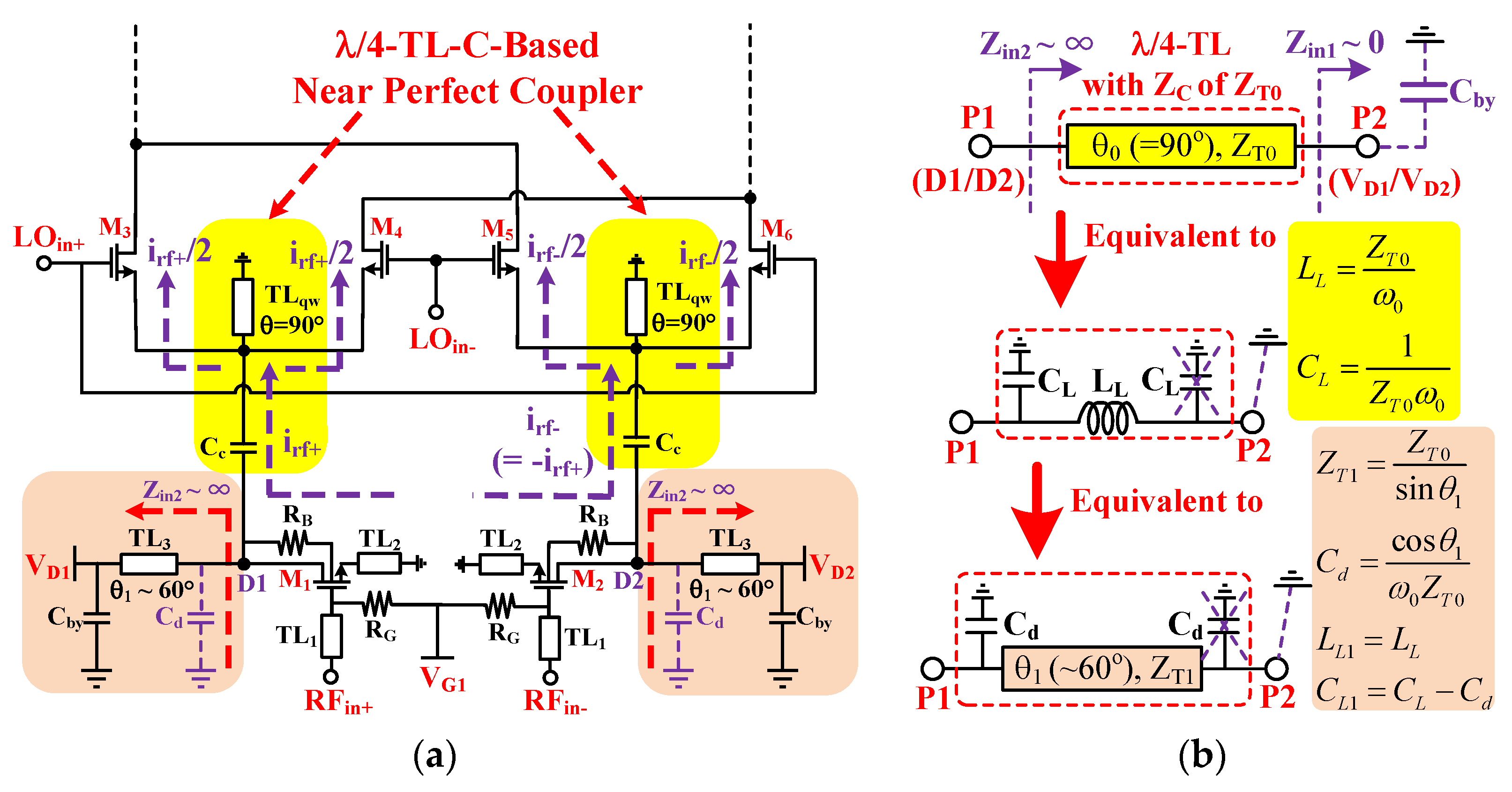
Figure 1a shows the illustrative diagram of the proposed low-VDD and low-PDC down-conversion mixer. In theory, the Zin of a grounded lossless λ/4-TL (denoted TLqw) is infinite at the operation frequency of f0 (=ω0/2π) and the odd-harmonic frequencies (3f0, 5f0, etc.) and is zero at DC and the even-harmonic frequencies (2f0, 4f0, etc.). Instead of the transformer coupling approach [7], two λ/4-TL-C-based couplers are used to achieve near perfect coupling from the RF transconductance (gm) stage to the LO switch transistors. The λ/4-TL-C-based coupler has the merits of a straightforward design and layout, as well as harmonic suppression. The low VDD and optimized noise, gain, and linearity design of the mixer become possible due to the separate DC bias of the RF gm stage and the LO-transistors/IF loads. In brief, the bias currents of transistors M3/M4 and M5/M6 flow to the ground through TLqw instead of the RF gm stage or transformer secondary coil. The outputs of the RF gm stage transmit to M3/M4 and M5/M6 near perfect through the λ/4-TL-C-based couplers instead of direct transmit or the transformer coupling. This is the way to achieve low VDD and optimized design. Moreover, CCPT-RL-based core IF load is used for load-impedance (ZL)/CG enhancement while keeping a low PD and wide IF bandwidth. The BSFB technique, i.e., connection of the gm-stage transistors’ body to their drain via a large body resistance RB (13.1 kΩ in this work) is used for threshold voltage (Vth) and VDD reduction, in addition to substrate leakage suppression. CG and NF enhancement at the same or even a lower PD is achieved because of the lower VDD and higher gm due to larger overdrive voltage (Vov) or bias current [11].


Figure 1.
Illustrative diagrams of (a) a mixer using a λ/4-TL-C-based coupler, and (b) the current-source load. (c) Layout and (d) simulated results of the coupler.
Figure 1b shows the current-source-load design of the gm stage. A lossless TLqw with an electrical length (θ) of 90° and characteristic impedance (ZC) of ZT0, such as the one in Figure 1c (with ZT0 of 89.7 Ω), can be modeled by an inductance (LL) and two parallel end-capacitance (CL) as follows [12].
On the condition that Zin1 is equal to zero, Zin2 is infinite at ω0 since the parallel of LL and CL exhibits an infinite impedance at ω0 from Equations (1) and (2). In the design of the current-source load of the gm stage, the parasitic capacitance (Cd) at drain nodes D1/D2 of M1/M2 should be considered. In theory, a TLqw with ZC of ZT0 is equivalent to a TL (with smaller θ (of θ1), larger ZC (of ZT1), and the same inductance (LL1 = LL)) and two extra parallel end-capacitance Cd values (=CL − CL1). One of the required Cd values is provided by the parasitic Cd and the other has no effect (due to in parallel with a short-circuit). ZT1 and Cd are given by
Suppose ZT0 is 65 Ω, then LL is 369.6 pH and CL is 87.4 fF at f0 of 28 GHz according to Equations (1) and (2). From Equations (3) and (4), θ1 is 60° and ZT1 is 75.1 Ω due to a Cd equal to 43.7 fF in this work.
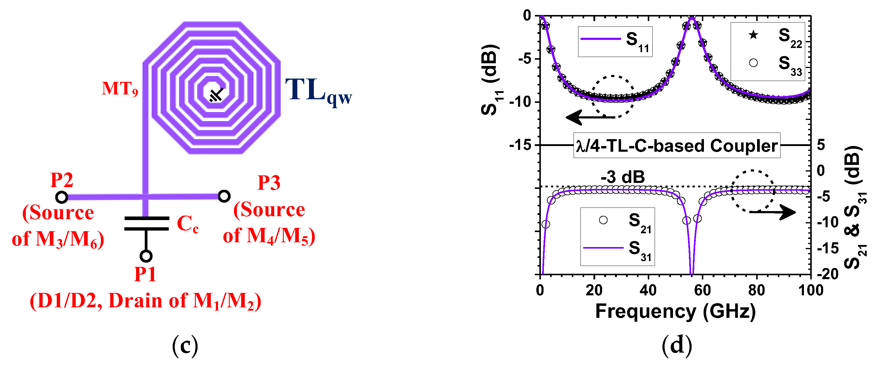
Figure 1c shows the simplified layout of the λ/4-TL-C-based coupler in Figure 1a. A compact spiral TLqw (with size of 73.6 × 76.1 μm2 and metal width/space of 3/2 μm) and a Cc (with size of 32 × 36 μm2 and equivalent capacitance of 1.76 pF) are used. Figure 1d shows the simulated reflection coefficients (S11, S22, and S33) and gain (S21 and S31) of the coupler. The coupler achieves decent S21 and S31 of −3.595 dB at 28 GHz and S21 and S31 better than −4 dB for 8.7–46.9 GHz. At 56 GHz, decent second-harmonic suppression (S11 of −0.22 dB, S22 and S33 of 0 dB, and S21 and S31 of −89 dB) is achieved.
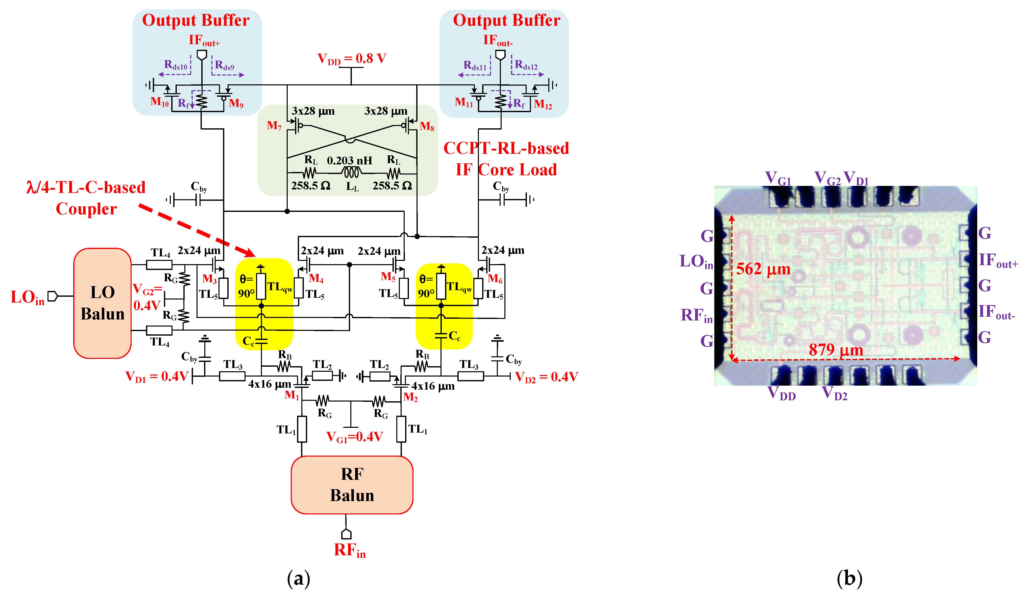
Figure 2a,b show the circuit diagram and chip of the down-conversion mixer with the important component parameters labeled. The chip area is 0.879 × 0.562 mm2, i.e., 0.494 mm2. The mixer comprises a double-balanced Gilbert-cell-based mixer core (with a differential RF gm stage using the BSFB technique, two λ/4-TL-C-based couplers, and a CCPT-RL-based core IF load), two Wilkinson-power-divider-based baluns, and differential output buffer amplifiers. The mixer was designed and implemented in 90 nm CMOS. This process offers nine metal layers, named MT1 to MT9 from bottom to top. The interconnection lines, as well as the TL inductors, were implemented with the 3.4 μm-thick upmost metal (MT9) to minimize the resistive loss. The Momentum three-dimensional (3D)-planar EM simulator in ADS (Advanced Design System) is used for EM-circuit cosimulation. Substrate and layer parameters of ADS Momentum are set up according to the process information provided by the foundry. This ensures the post-layout simulation results of the mixer close to the measurement ones. Instead of the transformer coupling approach (with a pair of λ/4 TLs for harmonic suppression) [7], a straightforward λ/4-TL-C-based coupler introduced in Figure 1 is used between the RF gm stage and the LO switch transistors. The BSFB technique, also shown in Figure 1, is used in the RF gm stage for Vth and VDD reduction, as well as substrate leakage suppression. CG and NF enhancement at the same or even lower PD is achieved because lower VDD and higher gm (due to larger bias current) are used. To enhance ZL/CG and keep a low PD and decent IF bandwidth, a CCPT-RL-based core IF load is used. At VDD = 0.8 V and VD1 = VD2 = VG1 = VG2 = 0.4 V, the mixer dissipates 6.4 mW. Compared with the traditional mixer for the direct-conversion receiver, the mixer consumes low PD and achieves significant CG and NF enhancement.
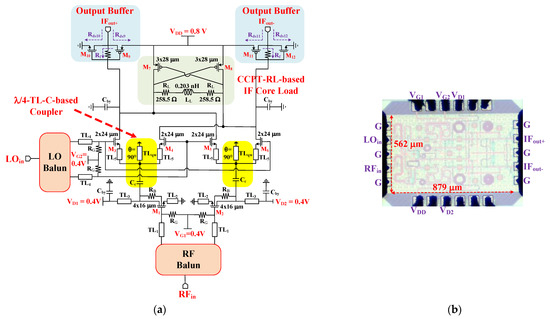
Figure 2.
(a) Schematic diagram, and (b) chip photo of the down-conversion mixer.
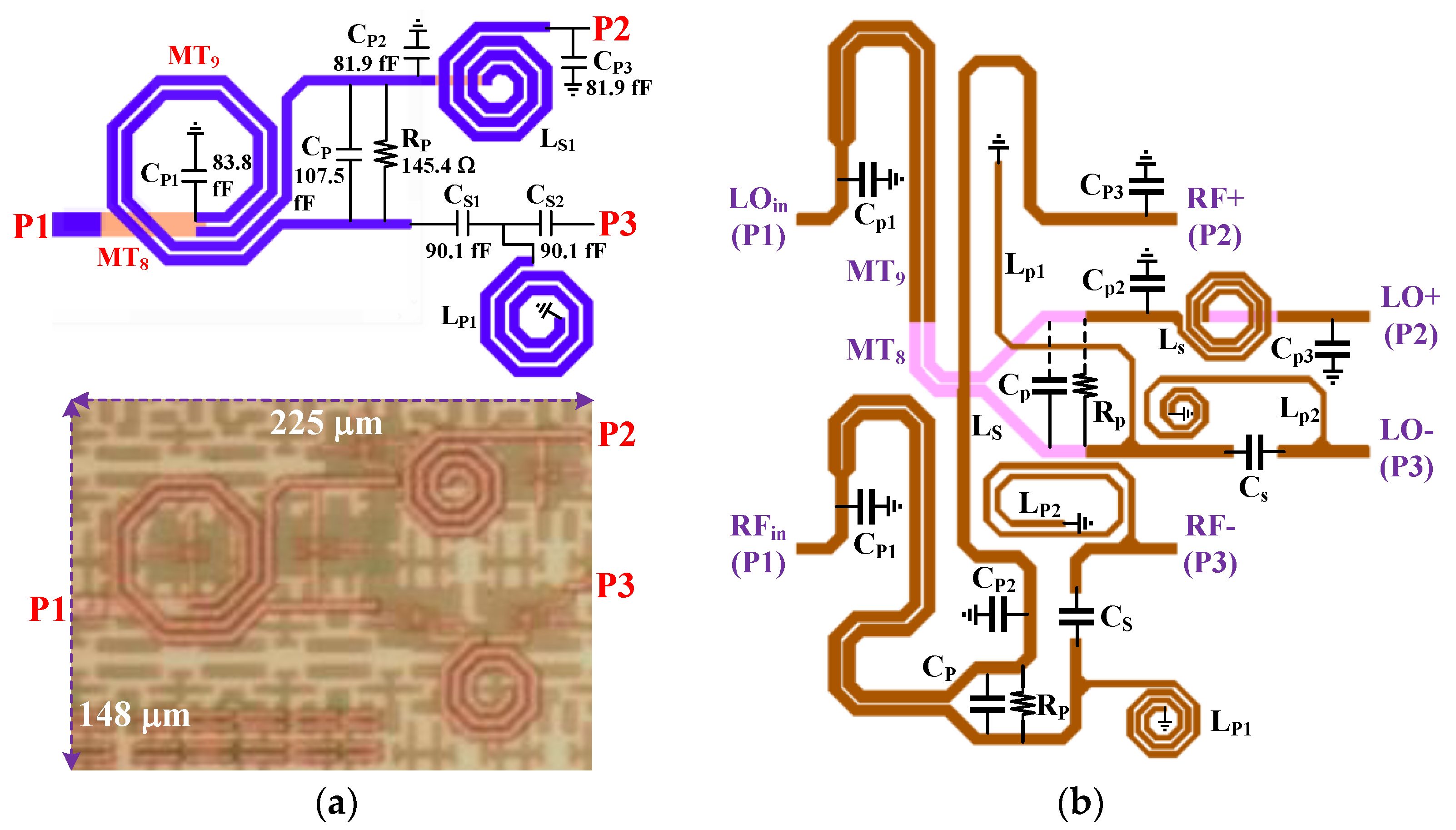
Figure 3 presents the illustrative diagram of the 28 GHz-band Wilkinson-power-divider-based balun [12]. It is used as the RF and the LO baluns. The compact Wilkinson power divider constitutes a noninverting coupled line with an electrical length (θ) of 22°, a parallel grounded capacitance CP1 at the input, and a parallel RPCP between the outputs. The coupled line, i.e., two noninverting spiral or meandering TLs with inductance of LL, has a positive mutual inductance (M) and an equivalent parallel inductance LP (=LL(LL − 2M)/M) between the outputs. This leads to a significant TL-length reduction (from about λ/10 to λ/16) for the power divider. The effect of LP can be cancelled by Cm (=M/[ω02LL(LL − 2M)]) in Figure 3. The π-network comprised of CP2, LS1, and CP3 introduces a phase delay of 90°, while the T-network comprised of CS1, LP1, and CS2 (or the π-network comprised of LP2, CS3, and LP3) introduces a phase lead of 90°. This is the way to achieve balun operation of the device.
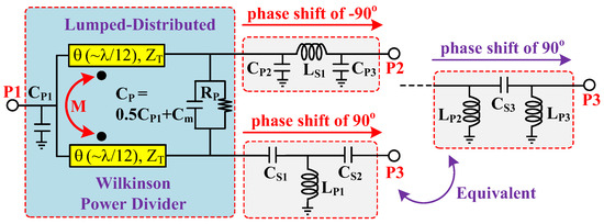
Figure 3.
Illustrative diagram of the power-divider-based balun.
Shown in Figure 4a is the simplified layout and chip photo of the first test balun, balun-1. A spiral layout is used for LS1 and LP1 in order to achieve a compact size. Balun-1 occupies a chip area of only 0.225 × 0.148 mm2, i.e., 0.033 mm2. Figure 4b shows the simplified layout of the RF and the LO baluns (i.e., dual balun-2) of the down-conversion mixer in this work. A symmetrical layout is crucial for the differential mixer core to attain good port-to-port isolation and overall performance. Therefore, the dual-balun-2 layout in Figure 4b is used to fit the symmetrical layout of the mixer core. The dual balun-2 occupies a chip area of 0.089 mm2. According to our previous experience, measured results of mm-wave passive devices are consistent with the simulated results of the EM simulator HFSS and ADS Momentum [13]. To expedite the realization of the down-conversion mixer, tape-out of the mixer is conducted based on the EM-circuit cosimulation result of the layout, i.e., post-layout simulation result, via ADS Momentum. Therefore, tape-out of the test device of dual balun-2 was not performed.
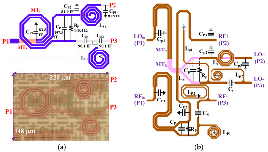
Figure 4.
(a) Layout and chip photo of balun-1. (b) Layout of dual balun-2.
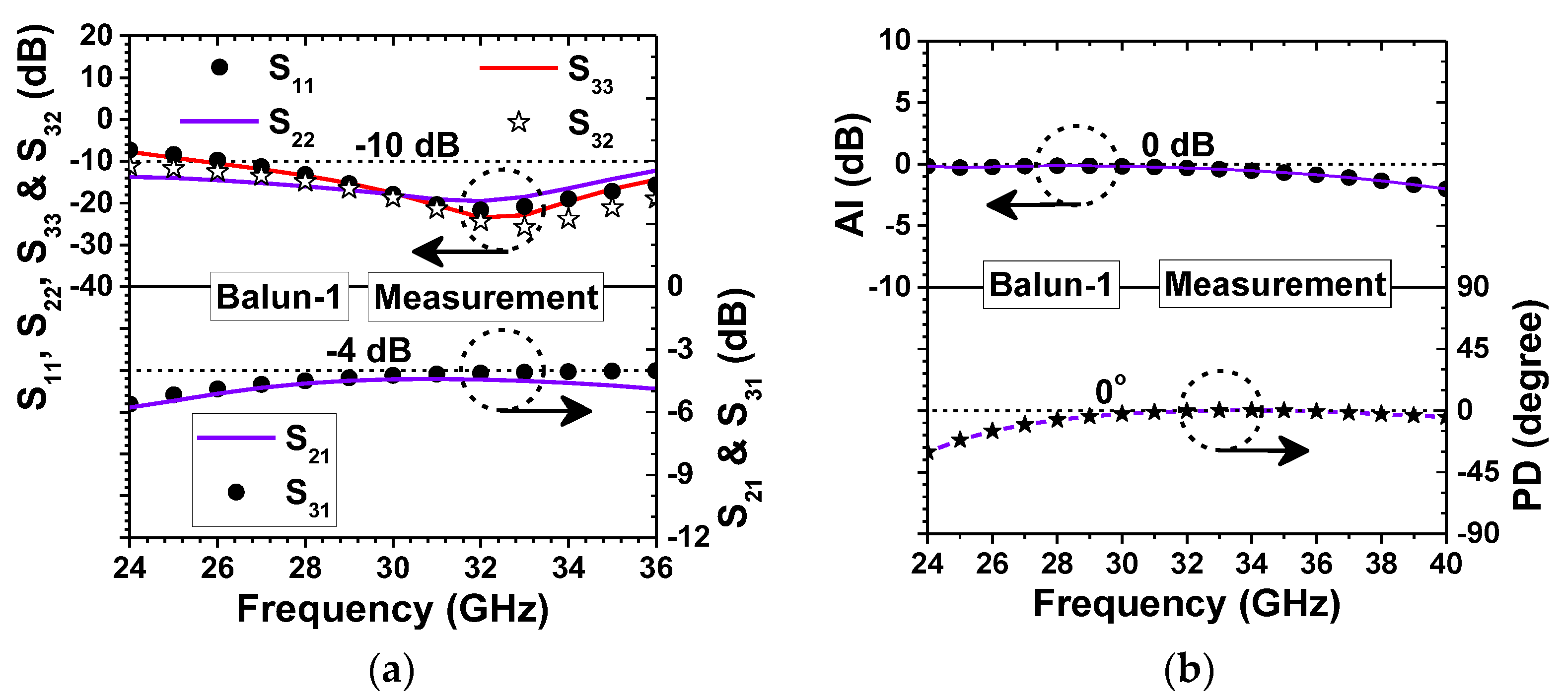
The measured reflection coefficients (S11, S22, and S33), isolation between the outputs S32, and gain (S21 and S31) of balun-1 are shown in Figure 5a. Balun-1 achieves a local minimum S11 of −21.6 dB at 32 GHz and S11 better than −10 dB from 26.2 GHz to over 50 GHz. The corresponding −10 dB input, matching the bandwidth (f10dB), is wider than 23.8 GHz. Balun-1 achieves a local minimum S22 of −19.5 dB at 32 GHz and S22 better than −10 dB from DC to 36.7 GHz, equivalent to an f10dB of 36.7 GHz. Balun-1 achieves a minimum S33 of −23.4 dB at 32 GHz and S33 better than −10 dB for 25.7–39.7 GHz, equivalent to an f10dB of 14 GHz. Moreover, balun-1 attains a local minimum S32 of −25.7 dB at 33 GHz and S32 better than −10 dB from DC to over 50 GHz, equivalent to a −10 dB isolation bandwidth (f10dB,iso) wider than 50 GHz. Balun-1 achieves S21 of −4.441 dB at 32 GHz and S21 better than −5 dB for 26.3–36.7 GHz, close to the measured S31 (−4.131 dB at 32 GHz, and better than −5 dB from 25.5 GHz to over 50 GHz).
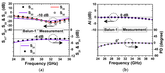
Figure 5.
Measured (a) S-parameters, and (b) AI and PD of balun-1.
Figure 5b shows the measured amplitude imbalance AI (equal to S21(dB) − S31(dB)) and phase deviation PD (equal to S21(degree) − S31(degree) − 180°) of balun-1. Balun-1 achieves the best AI of −0.127 dB at 28 GHz and AI within ±1 dB for 22.2–36.7 GHz, as well as the best PD of −0.08° at 35 GHz and PD within ±5° for 28.6–40.3 GHz. Compared to that with the commonly used Marchand balun with poor S22, S33, and S32 (of −6 dB in theory) [8], better overall performance is achieved.
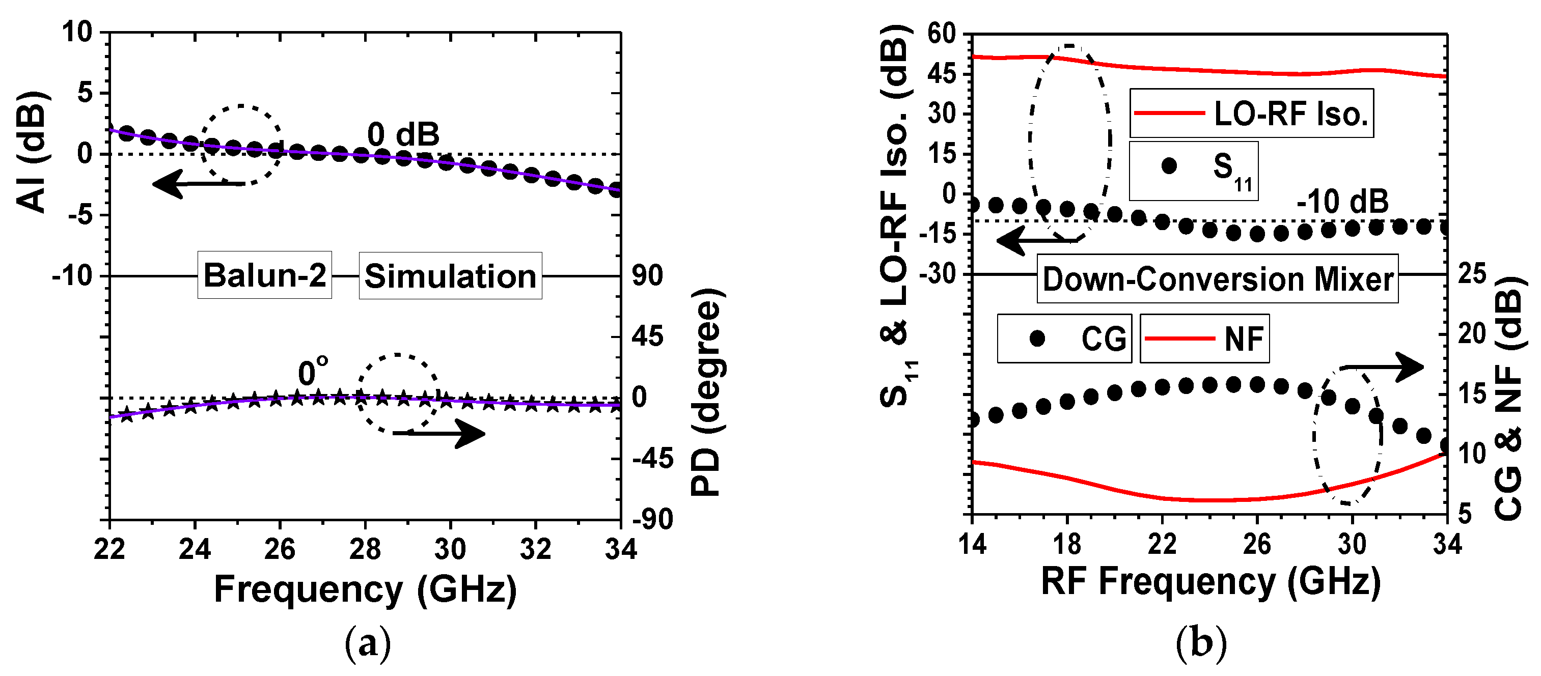
Figure 6a shows the simulated AI and PD of balun-2. Balun-2 attains the best AI of 0 dB at 27.5 GHz and AI within ±1 dB for 23.5–30.6 GHz, as well as the best PD of 0° at 26.4 GHz and PD within ±5° for 24.1–32.6 GHz. Figure 6b shows the simulated RF-port reflection coefficient (S11), LO–RF isolation, CG, and NF of the mixer. The mixer achieves a minimum S11 of −32.9 dB at 39 GHz and S11 better than −10 dB for 21.7–44.5 GHz (i.e., f10dB of 22.8 GHz). The good S11 is attributed to the decent input matching of the balun (see Figure 5a) and good matching between the balun outputs and the differential RF inputs. Due to the symmetrical layout and Cby of the mixer core, the mixer achieves decent LO–RF isolation of 44.9 dB at 28 GHz and 40.3–62.4 dB for 0–50 GHz. Moreover, the mixer achieves a maximum CG of 15.8 dB at 26 GHz and CG of 14.3 ± 1.5 dB for 14.3–32.5 GHz (i.e., f3dB of 18.2 GHz). The decent CG and f3dB are attributed to the CCPT-RL-based core IF load and the gain-enhanced gm stage. The mixer achieves a minimum NF of 6.2 dB at 24 GHz and NF of 6.2–9.3 dB for 14–33 GHz. The good NF of the mixer is attributed to its high CG and simultaneous noise and Zin matching of the gm stage.
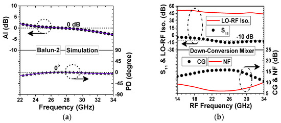
Figure 6.
Simulated (a) AI and PD of balun-2, and (b) S11, LO–RF isolation, CG, and NF of the down-conversion mixer.
3. Results
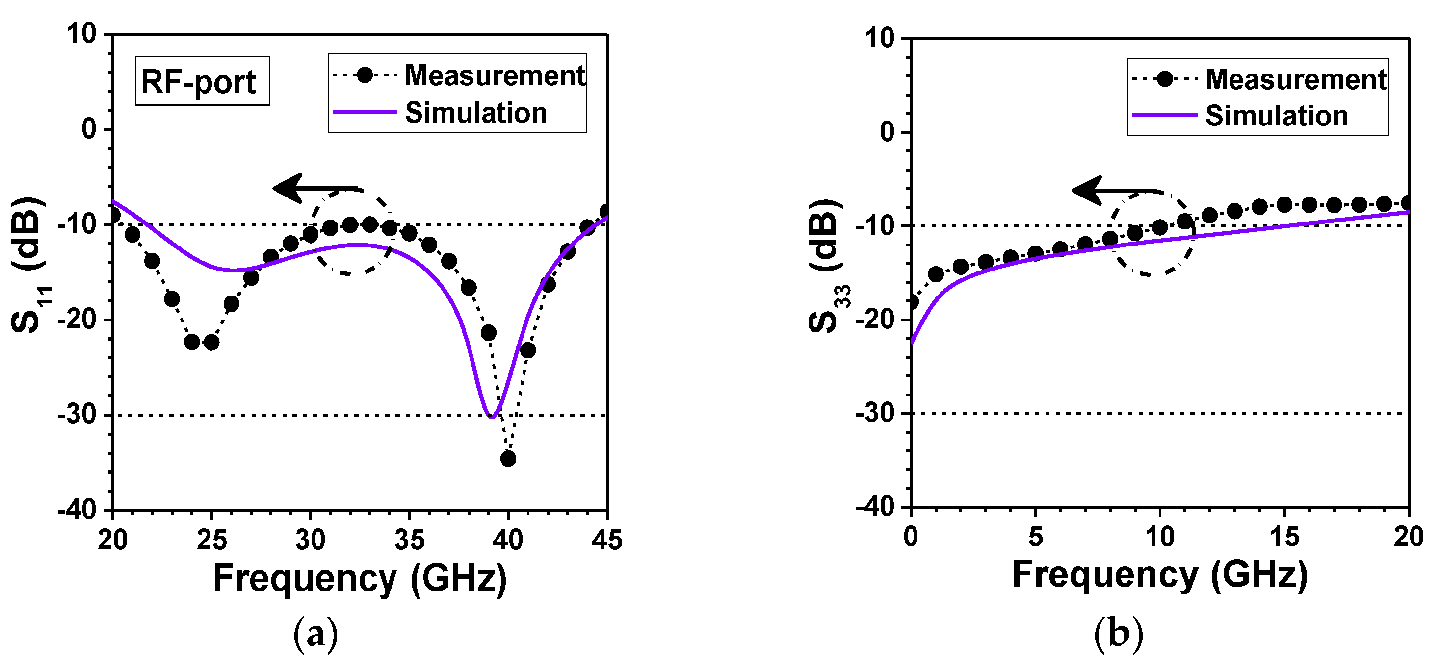
At VDD = 0.8 V and VD1 = VD2 = VG1 = VG2 = 0.4 V, the down-conversion mixer dissipates 6.5 mW, close to the simulated one (6.4 mW). The on-wafer S-parameter measurement of the mixer was conducted using a Keysight N5245B four-port PNA network analyzer (0.01–50 GHz). Figure 7a shows the measured and simulated RF-port reflection coefficient (S11) of the mixer. The mixer achieves a measured minimum S11 of −34.6 dB at 40 GHz and S11 better than −10 dB for 20.4–44.2 GHz (i.e., f10dB of 23.8 GHz), close to the simulated result (minimum S11 of −32.9 dB at 39 GHz and f10dB of 22.8 GHz (21.7–44.5 GHz)). For a mixer or amplifier using series RLC resonance matching, its f10dB (50/(3πLin) in theory) is inversely proportional to the input inductance Lin [14,15]. For the differential RF inputs, Lin (i.e., sum of the inductance of TL1 and TL2) is 435 pH, equivalent to f10dB of 12.2 GHz. The wideband S11 of the mixer is attributed to the wideband matching between the RF-balun outputs and the RF inputs due to the small Lin at RF inputs. Figure 7b shows the measured and simulated IF+ port reflection coefficient (S33) of the mixer. The mixer achieves a measured S33 better than −10 dB for 0–10.2 GHz (i.e., f10dB of 10.2 GHz), close to the simulated one (f10dB of 15.1 GHz (0–15.1 GHz)). The wideband S33 is attributed to the Zin matching at low frequency (LF) since the design values of Rds9llRds10llRf and Rds11llRds12llRf are 50 Ω. The slight deviation of the measured S11 and S33 (from the simulated ones) of the down-conversion mixer is mainly attributed to the substrate- and layout-layer parameters provided by the foundry being not accurate enough at mm-wave frequencies.
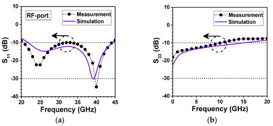
Figure 7.
Measured and simulated (a) S11, and (b) S33 of the mixer.
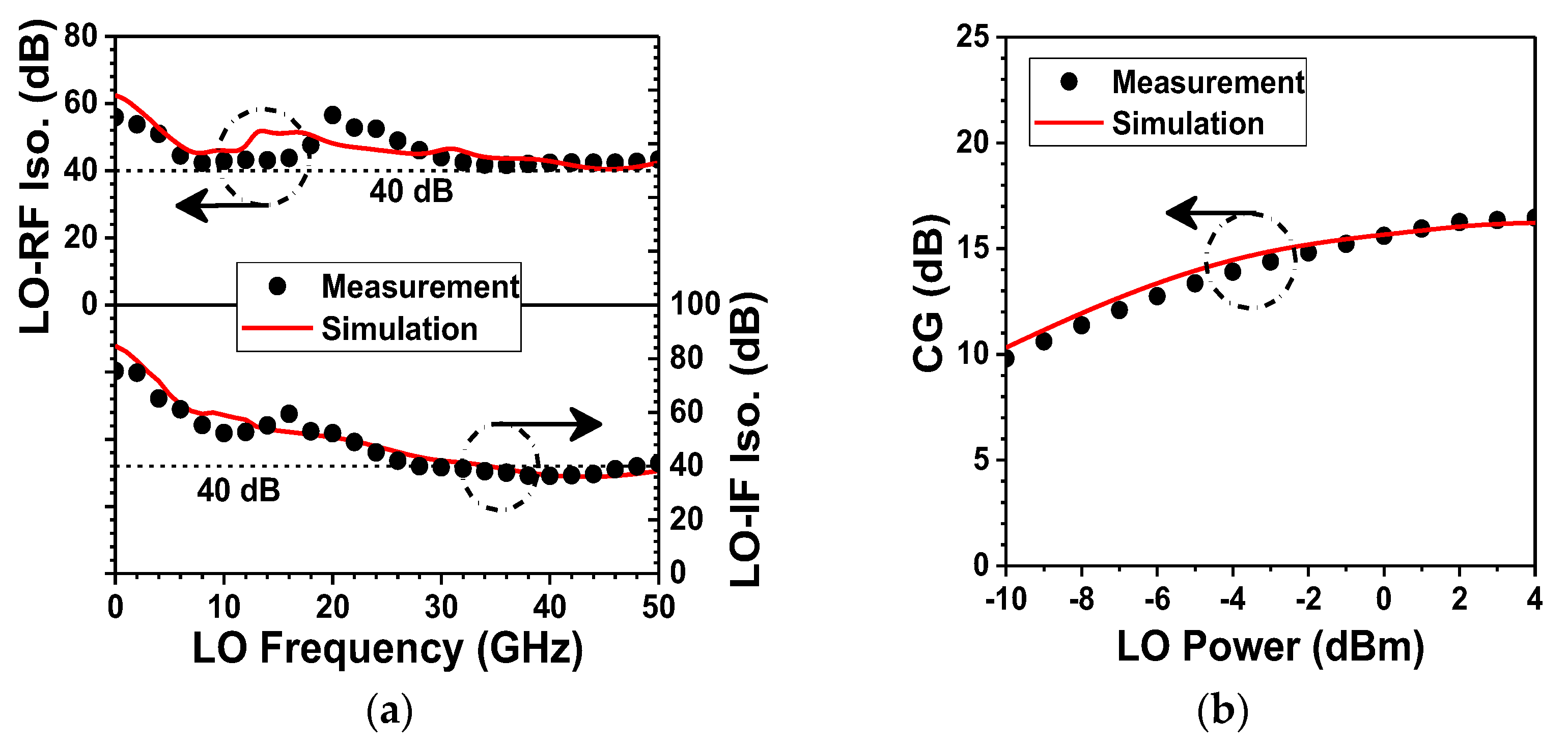
Figure 8a shows the measured and simulated LO–RF and LO–IF isolation versus LO frequency characteristics of the mixer. The mixer achieves measured LO–RF isolation of 46.1 dB at 28 GHz and 41.6–55.9 dB for 0–50 GHz, close to the simulated one (44.9 dB at 28 GHz, and 40.3–62.4 dB for 0–50 GHz). Since the Miller capacitance (of Cgd) at D1/D2 of M1/M2 has been taken into account in the Cd calculation, the decent LO–RF isolation is attributed to the symmetrical layout of the mixer core, and unilaterilization of the Cgd effect of M1/M2. Moreover, the mixer achieves measured LO–IF isolation of 39.9 dB at 28 GHz and 36.6–82.7 dB for 0–50 GHz, close to the simulated one (43.3 dB at 28 GHz, and 36–84.8 dB for 0–50 GHz). The decent LO–IF isolation (especially at LF) is attributed to the symmetrical layout of the mixer core and the inclusion of Cby between M3/M5 and M9/M10 (and M4/M6 and M11/M12) for low-pass filtering of the LO leakage. In brief, LO leakage around f0 is suppressed by Cby. Therefore, LF (around DC) leakage at the IF output is minimized due to the effective suppression of the second-order nonlinearity of the CCPT-RL-based core IF load and the output buffer amplifiers. Figure 8b shows the measured and simulated CG versus LOin characteristics of the mixer at 28 GHz. Intrinsically, the mixer is a nonlinear multiplier. Hence, it is reasonable that the CG of the mixer increases with the increase in LOin until saturation of the LO switch transistors (i.e., close to perfect switch operation). At LOin of 0 dBm, the mixer achieves a measured/simulated CG of 15.6/15.7 dBm, close to those (16.6/16.2 dBm) at LOin of 4 dBm. This indicates that LOin of 0 dBm is a reasonable choice for the switch operation of the LO switch transistors.

Figure 8.
Measured and simulated (a) LO–RF and LO–IF isolation versus LO frequency, and (b) CG versus LO input power characteristics of the mixer.
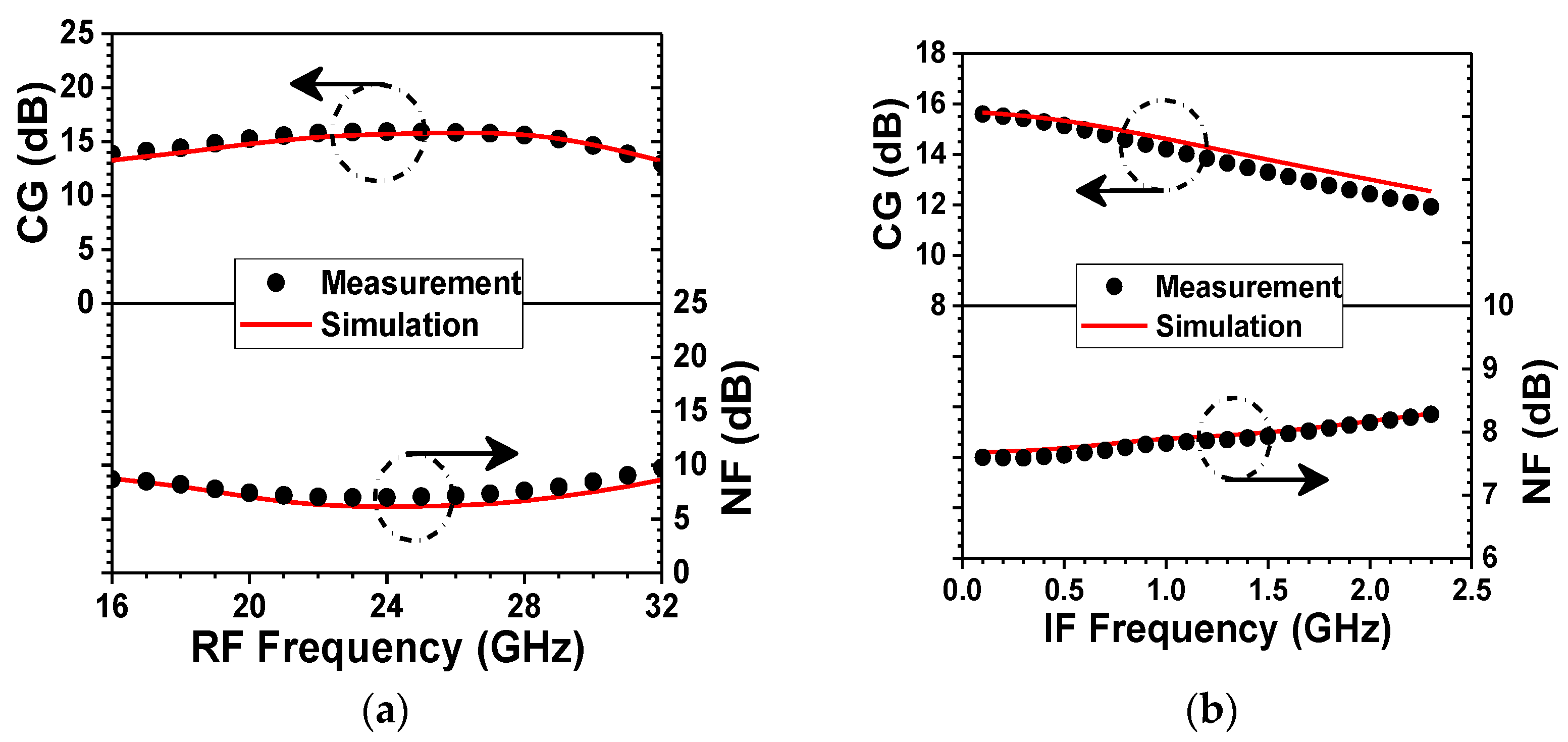
The on-wafer NF measurement was performed using an Agilent N8975A noise figure analyzer (0.01–26.5 GHz). An Agilent 1–50 GHz noise source with a 7–20 dB excess noise ratio (ENR) is used at the RF input. The LO input signal is provided by an Agilent E8257D signal generator (up to 67 GHz). Figure 9a shows the measured and simulated CG and NF versus RF frequency characteristics of the mixer. IF frequency is fixed at 0.1 GHz. The mixer achieves a measured CG of 15.6 dB at 28 GHz and CG of 14.4 ± 1.5 dB for 12.4–32 GHz, corresponding to an f3dB of 19.6 GHz. The result is close to the simulated CG (15.7 dB at 28 GHz and 14.3 ± 1.5 dB for 14.3–32.5 GHz, corresponding to an f3dB of 18.2 GHz). The broadband CG of the mixer is attributed to the wideband RF- and LO-port Zin matching (S11 and S22) and near perfect wideband-coupling of the λ/4-TL-C-based coupler. Moreover, the mixer achieves a measured NF of 7.6 dB at 28 GHz and 7–9.7 dB for 12.4–32 GHz, close to the simulated NF (6.7 dB at 28 GHz and 6.2–9.3 dB for 12.4–33 GHz). Figure 9b shows the measured and simulated CG and NF versus IF frequency characteristics of the mixer. The mixer achieves a measured CG of 15.6–12.6 dB for 0.1–1.9 GHz. The 3 dB IF bandwidth (f3dB,IF) is 1.9 GHz, wider than the required 1.5 GHz for 5G NR band N257 (28 ± 1.5 GHz) application. The result is close to the simulated one (15.7–12.7 dB for 0.1–2.2 GHz, i.e., f3dB,IF of 2.2 GHz). The mixer achieves a measured NF of 7.6–8.1 dB for 0.1–1.9 GHz, close to the simulated one (7.7–8.3 dB for 0.1–2.2 GHz). Furthermore, the mixer achieves a decent P1dB and IIP3 of −10.6 dBm and −1 dBm, respectively. For a larger VDD of 1 V, a better IIP3 of 1 dBm is achieved (not shown here).

Figure 9.
Measured and simulated (a) CG and NF versus RF frequency, and (b) CG and NF versus IF frequency characteristics of the mixer.
Table 1 is a summary of the 28 GHz down-conversion mixer and recently reported state-of-the-art mm-wave CMOS down-conversion mixers [1,2,3,4,5,6,7]. As can be seen, the mixer in this work is designed and implemented via a relatively cost-effective 90 nm CMOS process and achieves better overall performance than the mixer implemented with the costlier 40 nm CMOS technology in [6]. If a more advanced CMOS process is used for the mixer in this work, the overall performance can be further enhanced. This means that the proposed down-conversion mixer architecture has high potential for mm-wave communication systems. Overall, compared with that in [1,2,3,4,5,6,7], our mixer occupies a medium chip area, requires a medium LOin, consumes low power, and achieves prominent CG, f3dB, NF, LO–RF isolation, and IIP, and one of the best FOM1s and FOM2s. The remarkable results indicate that the proposed down-conversion mixer architecture is suitable for 28 GHz 5G NR and even a higher frequency system.

Table 1.
Summary of the down-conversion mixer and recently reported state-of-the-art mm-wave down-conversion mixers.
Finally, it would be informative to provide readers with a futuristic vision about what the future holds for us as we move forward [16,17,18,19]. Considering the saturation of the state-of-the-art microelectronic technologies in providing a faster operation speed, nowadays, hybrid optoelectronic platforms are considered a new solution to expand the operation bandwidth, while we can still enjoy the CMOS technology for implementing such hybrid systems. One direction that is gaining large momentum in the field is the utilization of hot-electron optoelectronic nano-devices. This concept relies on the fact that metals have an abundance of free electrons, so they can nicely capture light if they are fashioned as a nanoscale optical antenna. In addition, employing metals is a necessary part of electronic circuits, e.g., as electrical contacts. Therefore, if meticulously designed, a nano-metal with optical antenna properties can be used as an electrical contact as well; therefore, one can access the hot electrons in metals for optoelectronic applications [16]. Such hot carriers can enable the extremely fast switching of electrical signals [17]. In a capacitor configuration, such high-energy hot electrons have the possibility of being transported over a Schottky barrier in a very short timeframe. The injection of hot carriers into a dielectric/oxide/air material will change its conductivity in a very short timescale, thereby allowing for ultrafast optoelectronic switching, which is inherently a frequency down conversion process. The beauty of this technique is hidden in the fact that hot-electron optoelectronic systems do not rely on the absorption of light in a semiconductor. Therefore, practically any oxide or metal combination can be employed to produce a hot-electron optoelectronic convertor without being concerned about the intrinsic properties of employed materials or a capacitive nature of the circuit, which limits the bandwidth. Initial demonstrations of such switches were proposed recently [18,19]. However, practical devices are yet to be demonstrated.
4. Conclusions
We demonstrate a 6.5 mW 12.4–32 GHz CMOS down-conversion mixer with a decent CG of 14.4 ± 1.5 dB and NF of 7–9.7 dB for 28 GHz 5G NR. A λ/4-TL-C-based coupler is used for harmonic suppression and near-perfect coupling from the RF gm stage to the LO switch transistors. The BSFB technique is used for Vth and VDD reduction. The CCPT-RL-based core IF load is used for ZL (i.e., CG) and f3dB,IF boosting. CG and NF enhancement at the same (or even a lower) PDC is achieved due to a lower VDD and higher gm and ZL. As a result, low PDC and optimized CG, NF, and linearity are achieved for the mixer due to the separate bias (i.e., optimized design) of the gm stage and the IF loads.
Author Contributions
Conceptualization, Y.-S.L. and K.-S.L.; methodology, Y.-S.L. and K.-S.L.; software, K.-S.L.; validation, Y.-S.L. and K.-S.L.; formal analysis, Y.-S.L.; investigation, Y.-S.L.; resources, Y.-S.L.; data curation, K.-S.L.; writing—original draft preparation, K.-S.L.; writing—review and editing, Y.-S.L.; visualization, Y.-S.L.; supervision, Y.-S.L.; project administration, Y.-S.L.; funding acquisition, Y.-S.L. All authors have read and agreed to the published version of the manuscript.
Funding
This research was funded by the National Science and Technology Council (NSTC), Taiwan, grant number MOST111-2221-E-260-017.
Institutional Review Board Statement
Not applicable.
Informed Consent Statement
Not applicable.
Data Availability Statement
Not applicable.
Acknowledgments
This work was supported by the National Science and Technology Council (NSTC) of Taiwan under Contract MOST111-2221-E-260-017. The authors would like to thank the Taiwan Semiconductor Research Institute (TSRI) for the support of chip fabrication and measurements.
Conflicts of Interest
The authors declare no conflict of interest.
References
- Chang, Y.T.; Lin, K.Y. A 28-GHz bidirectional active Gilbert-cell mixer in 90-nm CMOS. IEEE Microw. Wirel. Compon. Lett. 2021, 31, 473–476. [Google Scholar] [CrossRef]
- Bae, B.; Han, J. 24–40 GHz gain-boosted wideband CMOS down-conversion mixer employing body-effect control for 5G NR applications. IEEE Trans. Circuits Syst. II Express Briefs 2022, 69, 1034–1038. [Google Scholar] [CrossRef]
- Peng, Y.; He, J.; Hou, H.; Wang, H.; Chang, S.; Huang, Q.; Zhu, Y.A. K-Band high-gain and low-noise folded CMOS mixer using current-reuse and cross-coupled techniques. IEEE Access 2019, 7, 133218–133226. [Google Scholar] [CrossRef]
- Lin, H.H.; Lin, Y.H.; Wang, H. A high linearity 24-GHz down-conversion mixer using distributed derivative superposition technique in 0.18-μm CMOS process. IEEE Microw. Wirel. Compon. Lett. 2018, 28, 49–51. [Google Scholar] [CrossRef]
- Chang, Y.T.; Kang, C.Y.; Lu, H.C. A V-band high-gain sub-harmonic down-conversion mixer using PMOS cross couple pair to implement negative impedance and current-bleeding technique. IEEE Trans. Circuits Syst. II Express Briefs 2021, 68, 2765–2769. [Google Scholar] [CrossRef]
- Chang, Y.T.; Lu, H.C. A V-Band ultra low power sub-harmonic I/Q down-conversion mixer using current re-used technique. IEEE Trans. Circuits Syst. II Express Briefs 2020, 67, 2893–2897. [Google Scholar]
- Liu, Z.; Dong, J.; Chen, Z.; Jiang, Z.; Liu, P.; Wu, Y.; Zhao, C.; Kang, K. A 62–90 GHz high linearity and low noise CMOS mixer using transformer-coupling cascode topology. IEEE Access 2018, 6, 19338–19344. [Google Scholar] [CrossRef]
- Lin, Y.S.; Wang, Y.E. Design and analysis of a 94-GHz CMOS down-conversion mixer with CCPT-RL-based IF Load. IEEE Trans. Circuits Syst.-I: Regul. Pap. 2019, 66, 3148–3161. [Google Scholar] [CrossRef]
- El-Nozahi, M.; Sanchez-Sinencio, E.; Entesari, K. A 20–32-GHz wideband mixer with 12-GHz IF bandwidth in 0.18 μm SiGe process. IEEE Trans. Microw. Theory Tech. 2010, 58, 2731–2740. [Google Scholar] [CrossRef]
- Guan, X.; Hajimiri, A. A 62–90 GHz high linearity and low noise CMOS mixer using transformer-coupling cascode topology. IEEE J. Solid-State Circuits 2004, 39, 368–373. [Google Scholar] [CrossRef]
- Chang, J.F.; Lin, Y.S. 3–9 GHz CMOS LNA using body floating and self-bias technique for sub-6 GHz 5G communications. IEEE Microw. Wirel. Compon. Lett. 2021, 31, 608–611. [Google Scholar] [CrossRef]
- Lin, Y.S.; Lan, K.S. Realization of a compact and high-performance power divider using parallel RC isolation network. IEEE Trans. Circuits Syst. II Express Briefs 2021, 68, 1368–1372. [Google Scholar] [CrossRef]
- Lin, Y.S.; Nguyen, V.K. 94 GHz CMOS power amplifiers using miniature dual Y-shaped combiner with RL load. IEEE Trans. Circuits Syst. II Regular Papers 2017, 64, 1285–1298. [Google Scholar] [CrossRef]
- Wang, T.; Chen, H.C.; Chiu, H.W.; Lin, Y.S.; Huang, G.W.; Lu, S.S. Micromachined CMOS LNA and VCO by CMOS-compatible ICP deep trench technology. IEEE Trans. Microw. Theory Tech. 2006, 54, 580–588. [Google Scholar] [CrossRef]
- Lin, Y.S.; Chen, C.Z.; Yang, H.Y.; Chen, C.C.; Lee, J.H.; Huang, G.W.; Lu, S.S. Analysis and Design of a CMOS UWB LNA with Dual-RLC-Branch Wideband Input Matching Network. IEEE Trans. Microw. Theory Tech. 2010, 58, 287–296. [Google Scholar]
- Taghinejad, M.; Cai, W. All-Optical Control of Light in Micro- and Nanophotonics. ACS Photonics 2019, 6, 1082–1093. [Google Scholar] [CrossRef]
- Taghinejad, M.; Xu, Z.; Lee, K.T.; Lian, T.; Cai, W. Transient Second-Order Nonlinear Media: Breaking the Spatial Symmetry in the Time Domain via Hot-Electron Transfer. Phys. Rev. Lett. 2020, 124, 013901. [Google Scholar] [CrossRef] [PubMed]
- Ludwig, M.; Aguirregabiria, G.; Ritzkowsky, F.; Rybka, T.; Marinica, D.C.; Aizpurua, J.; Borisov, A.G.; Leitenstorfer, A.; Brida, D. Sub-femtosecond Electron Transport in a Nanoscale Gap. Nat. Phys. 2020, 16, 341–345. [Google Scholar] [CrossRef]
- Bionta, M.R.; Ritzkowsky, F.; Turchetti, M.; Yang, Y.; Mor, D.C.; Putnam, W.P.; Kärtner, F.X.; Berggren, K.K.; Keathley, P.D. On-chip Sampling of Optical Fields with Attosecond Resolution. Nat. Photonics 2021, 15, 456–460. [Google Scholar] [CrossRef]

Disclaimer/Publisher’s Note: The statements, opinions and data contained in all publications are solely those of the individual author(s) and contributor(s) and not of MDPI and/or the editor(s). MDPI and/or the editor(s) disclaim responsibility for any injury to people or property resulting from any ideas, methods, instructions or products referred to in the content. |
© 2023 by the authors. Licensee MDPI, Basel, Switzerland. This article is an open access article distributed under the terms and conditions of the Creative Commons Attribution (CC BY) license (https://creativecommons.org/licenses/by/4.0/).