Communication

16-Channel Wavelength Division Multiplexers Based on Subwavelength Grating

1
State Key Laboratory of Transient Optics and Photonics, Xi’an Institute of Optics and Precision Mechanics, Chinese Academy of Sciences (CAS), Xi’an 710119, China
2
Center of Materials Science and Optoelectronics Engineering, University of Chinese Academy of Sciences, Beijing 100049, China
3
Zhejiang Lab, Hangzhou 311100, China
*
Authors to whom correspondence should be addressed.
Appl. Sci. 2023, 13(3), 1833; https://doi.org/10.3390/app13031833
Submission received: 30 November 2022 / Revised: 15 January 2023 / Accepted: 29 January 2023 / Published: 31 January 2023
(This article belongs to the Special Issue Laser and Silicon Photonics: Technology, Preparation and Application)

Abstract

:
Wavelength Division Multiplexing (WDM) plays an important role in optical interconnection. In this paper, a 16-channel WDM device is designed on a Silicon-On-Insulator (SOI) substrate by using a sub-wavelength grating (SWG) structure, which can cover O-band and C-band at the same time, and the output channel is reversely coupled from the main waveguide to realize wavelength demultiplexing. The simulation results show that the loss of our 16-channel wavelength demultiplexing device is less than 0.5 dB and the crosstalk is less than 17 dB. When WDM is performed in O-band, the transmission loss of the C-band in the bus waveguide is less than 0.05 dB and is insensitive to the grating duty cycle, with good process tolerance. The footprint of the device is 200 μm × 150 μm, and the size of the single-channel filter is 200 μm × 2 μm, which can realize WDM with large bandwidth in a compact structure.

1. Introduction

With the development of technologies such as 5G, big data, the Internet of Things, cloud computing, and artificial intelligence, society’s demand for information transmission continues to grow exponentially. With the advantages of high speed, large bandwidth, low latency, and low power consumption, optical interconnection gradually replaces traditional electrical interconnection and becomes an effective way to solve massive data transmission, exchange, and processing, and is gradually applied to backbone network transmission and data centers, high-performance computing and sensing [1,2,3,4]. Silicon-based optoelectronics has become a key technology for optical communication and optical interconnecting due to its advantages of high integration, anti-electromagnetic interference, complementary metal oxide semiconductor (CMOS) process compatibility, low power consumption, and low cost [5,6,7,8,9,10]. In recent years, many advances have been made in silicon-based optoelectronic devices. Since silicon (Si) has a band gap of 1.19 eV and is transparent to the wavelengths of the communication band, silicon waveguides can transmit multiple wavelengths of light simultaneously and almost non-destructively. Multiple optical waves are transmitted and calculated on the chip at the same time, which can double the transmission rate and processing rate of the on-chip data. Among them, the application of wavelengths has doubled the transmission rate and processing rate of on-chip optical signals, and wavelength devices such as wavelength division multiplexers (WDMs) and filters have become research hotspots [11,12].
To achieve WDM on a chip, researchers designed a variety of structures, including array waveguide grating (AWG) [13,14], etched diffraction grating (EDG) [15], sub-wavelength grating (SWG) [16,17], cascaded Mach-Zender interference structures (MZI) [18], micro-ring resonators (MRR) [19,20], photonic crystal filters [21] sidewall gratings [22], etc. These wavelength devices are essentially based on the phase matching of light. Among these, SWG has the advantages of small size compared with other wave decomposition multiplexing devices, can achieve flat-top filtering, and there is no FSR limitation [23,24]. In recent years, researchers have conducted studies on SWG waveguide-based WDM, providing new ideas for improving the efficiency of on-chip data transmission [25,26].
In this paper, we designed and simulated a 16-channel wavelength WDM based on SWG. Different from the previously reported SWG-based WDM, our design utilizes an SWG perturbation structure to provide an inverse couple condition for each channel, which can lower the transmission loss and enhance fabrication tolerance compared to WDM on SWG waveguide structure. Besides, with specific structure optimization, our design is capable of 16-channel WDM, covering both O-band and C-band. Simulation results show that the 16-channel wavelength demultiplexer has a single-channel loss of less than 0.5 dB and crosstalk of less than 17 dB. When WDM is performed in the O-band, the loss of C-band is low in the bus waveguide, and the modified structure is insensitive to the duty cycle of the SWG, with a process tolerance of more than 20 nm. The single-channel filter has a size of 200 μm × 2 μm and an overall footprint of 200 μm × 150 μm, allowing for large bandwidth WDM in a compact structure.

2. Structure and Method

The 16-channel O- and C-band WDM we demonstrate are composed of SWG inverse couplers so that the two waveguide modes in opposite directions satisfy the phase matching condition to achieve coupling. The overall structure of the device is shown in Figure 1. There is the main waveguide and 16 coupling branches. The main waveguide is bent back and forth in an “s” shape to reduce the size of the device. There are eight output channels for each of the O-band and C-band, which are sequentially distributed on both sides of the device. The width of the waveguide and the period of the SWG determine the coupling conditions of the bus waveguide and the branch waveguide: the O-band adopts the strip waveguide as the bus waveguide and the SWG as the output channel; the C-band adopts the SWG as the bus waveguide and the strip waveguide as the output channel, such a structure The design can meet dual-band low-loss transmission. Filtering by SWG inverse coupling can achieve a flat-topped waveform, which is preferred in WDM. Broad-spectrum light is coupled into the device from the input port, and then the O-band WDM is performed. In our design, the O-band WDM can ensure low-loss transmission in the C-band. C-band WDM is performed following the O-band WDM to complete the O + C WDM. Theoretically, the bandwidth of this structure can be expanded arbitrarily, and here we demonstrate the WDM of 1280–1340 nm and 1520–1580 nm by simulation.
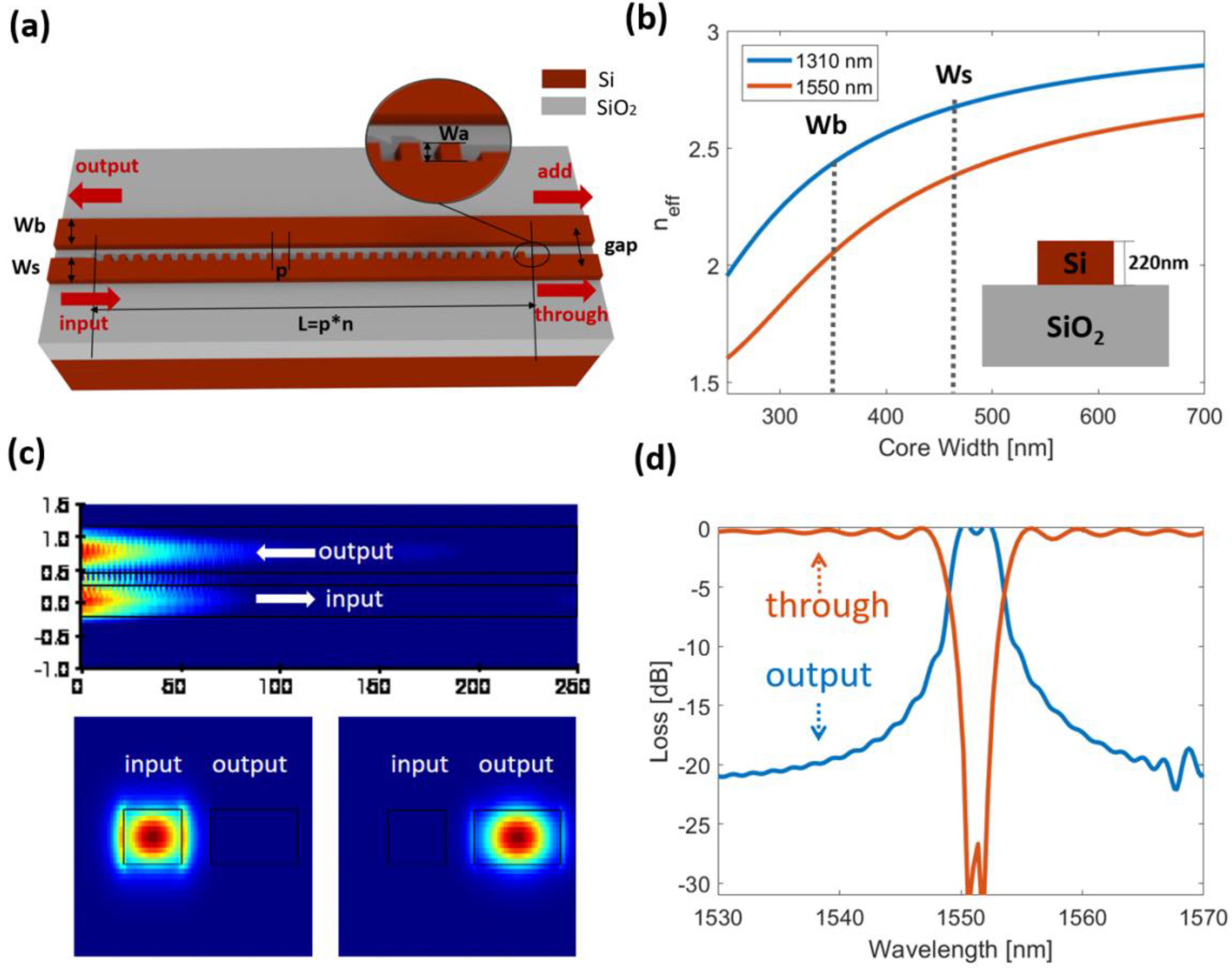
We use a grating perturbation inverse coupler for wavelength division. A single coupling structure is shown in Figure 2a. The waveguide with grating perturbation has a width of Ws, and the width of the strip waveguide is Wb. The internal reduction is reduced to form a perturbation structure with a modulation width of Wa. Such a structure can ensure that the average effective refractive index in one period of the grating perturbation region is not much different from that of a straight waveguide with a width of Ws, so that the wavelength drift is small, and results closer to the theoretical value can be obtained. Figure 2b shows the variation of the effective refractive index of the strip waveguide with the O-band and C-band thickness of 220 nm with the width of the waveguide. When there is no auxiliary grating, due to the different widths of Ws and Wb, the phase mismatch causes the co-coupling deadline. At this time, if a grating perturbation structure is added to one of the waveguides when the following conditions in Equation (1) are met, the matching of the propagation constants of the strip waveguide and the SWG-based perturbation waveguide can be achieved:
Δ β = β 1 + β 2 2 π m p = 0
Here, β1 and β2 are the propagation constants of the two waveguides, respectively, p is the grating period, m is an integer, and 2π/p is the grating vector. In addition, there is:
β = 2 π n e f f λ 0
where λ0 is our target wavelength. When m = 1, put Equation (2) into Equation (1) to get
n e f f 1 + n e f f 2 = λ 0 p
where neff1 and neff2 are the mode refractive index of the strip waveguide and the SWG-based perturbation waveguide, respectively. It can be seen that the period of the perturbation grating is related to the sum of the effective refractive index of the strip waveguides, and the grating period can be calculated from this. The bandwidth of a single channel is given by:
Δ λ = 2 λ 0 2 π ( n e f f 1 + n e f f 2 ) κ 2 + ( π L ) 2
It can be seen from Equation (4) that the bandwidth of single-channel filtering is mainly related to the sum of the mode-effective refractive index of the two waveguides, the coupling coefficient, and the coupling length. Among them, the coupling coefficient is mainly realized by the grating width and waveguide spacing, and the coupling length (the number of cycles) is determined. In this work, we demonstrate a WDM structure with a channel spacing of 5 nm, and this structure can be designed according to actual needs in specific applications.
The structure of a single filter is shown in Figure 2a. The WDM waveguide for reverse transmission can be either an SWG waveguide or a strip waveguide. Figure 2b simulates the effective refraction of a 220 nm thick Si waveguide at 1310 nm and 1550 nm. The curve of the rate is a function of the waveguide width. According to the waveguide width, after simulating the respective effective refractive index, the grating perturbation structure can be designed according to the needs to meet the corresponding filtering function. As shown in the figure, when Wb = 600 nm, Ws = 400 nm, neff1 = 2.570, neff2 = 2.229, at this time λ0 = 1.55 μm, p = 322.9 nm can be calculated from Equation (3), there will be some gaps between actual simulation and calculation, as appropriate. After adjustment, p = 319.4 nm, the duty cycle is 0.5, and Wa is 100 nm. The light field diagram at 1548–1552 nm is shown in Figure 2c shows the optical field diagram at 1548–1552 nm. It can be seen that Gaussian light with a bandwidth of 5 nm is input from the input port of Ws, almost completely back-coupled to the Wb waveguide, and output from the output port under phase-matching conditions. Figure 2d shows the transmission spectral lines of the through and output ports. the light output from the through port is transmitted to the next WDM channel with an insertion loss of less than 0.05 dB.
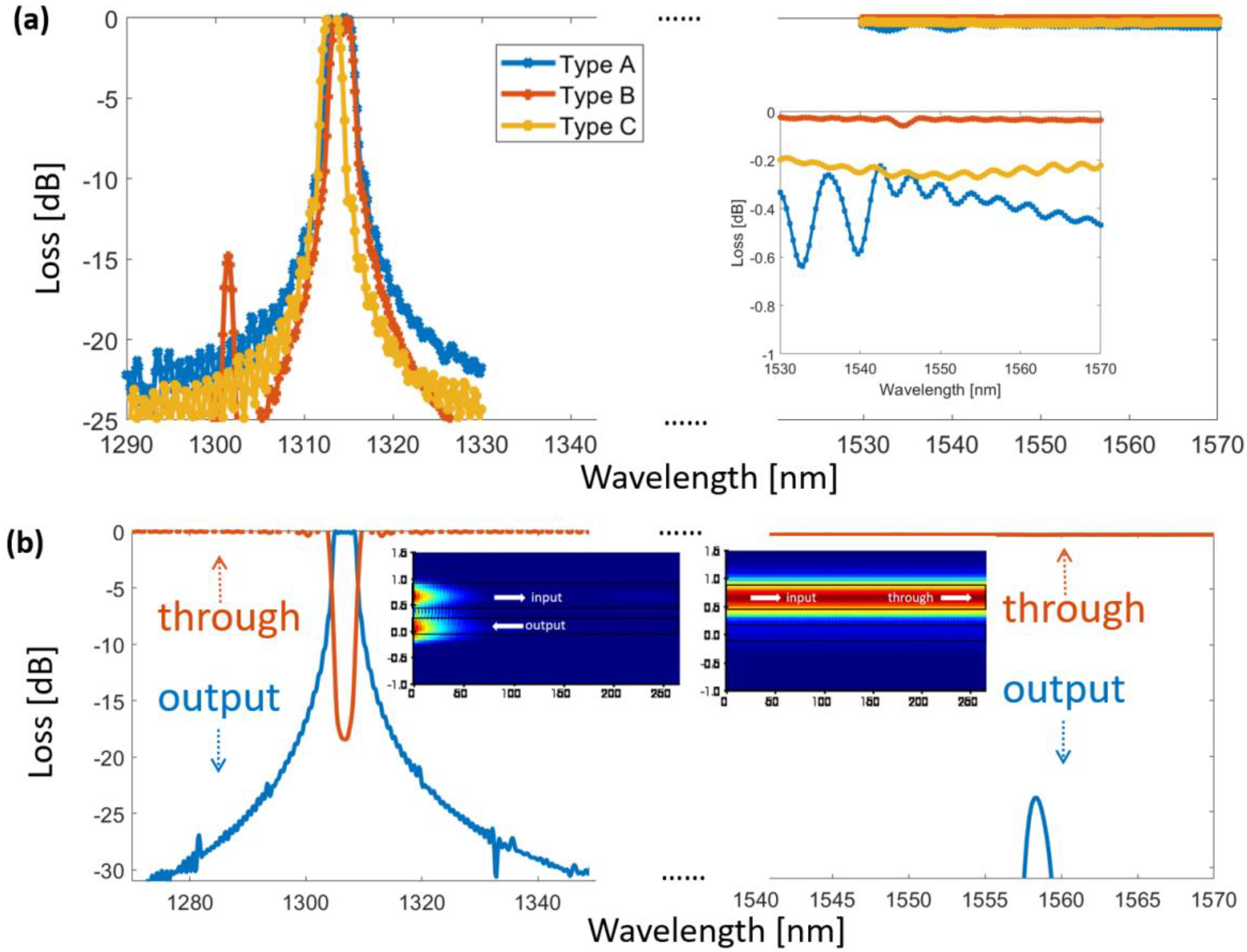
A low-loss C-band transmission should be obtained in the O-band WDM area. As shown in Figure 3a, the spectral lines of three different structures of SWG are demonstrated when transmitting O-band and C-band, and through simulation, we selected three SWG structures with good wavelength division performance at 1310 nm and their corresponding C-band simulation results. Since the structure parameters of each type are different, the Bragg wavelength is different. The Bragg wavelength of type B is around 1300 nm, which cause a decrease in the loss around 1300 nm for type B but not for types A and C. As shown in Figure 3b, for the same waveguide width (Wb or Ws), different wavelengths (λ1 = 1310 nm and λ2=1550 nm) will have different mode refractive indices, which will lead to different wave mismatch conditions. It is the coupling coefficient that determines whether the forward coupling of C-band will occur. The coupling coefficient is determined by the width of the grating, the waveguide interval, and the coupling length, by adjusting the width of Wb and Ws and the width of the grating disturbance Wa, so that when the O-band is reverse-coupled, the forward coupling coefficient of the C-band is low, and the output from through is almost lossless. As shown in Figure 3a, we optimized the loss in the C-band from 0.6 dB of type A to 0.05 dB of type B, while type A, B, and C represented different dimensional parameter setting of Ws, Wb, gap and p in our optimization process. The optimized O-band main line waveguide is a bar waveguide, and the back-coupled filter is an SWG waveguide. In contrast, the C-band is the SWG waveguide, and the back-filtered waveguide is the bar waveguide. At this time, the through and output port transmission lines of O and C are shown in Figure 3b, and the transmission light field diagram is embedded in the figure. The parameters for the O-band and C-band are shown in Table 1.
Table 1 shows the parameters of the central wavelength of the O-band and C-band. After multiple optimizations, we selected the grating with the above parameters for overall simulation to ensure the WDM performance of the O-band and C-band.

3. Results and Discussion

We designed and simulated a 16-channel wavelength WDM based on SWG, and the channel interval iwas 4 nm. We only needed to adjust the period to meet the wavelength shift, and Δλ/Δpitch hardly changed within the 40 nm bandwidth, which means that we could use the 3dB bandwidth of a single channel. The period of the perturbation grating can be fine-tuned, and the corresponding filter channel can also be designed according to the needs of the specific scene. We simulated the designed structure in FDTD Solutions with a PML boundary condition. The incident light wave was a TE0 broad-band source with wavelength from 1290 nm to 1570 nm. The light wave of different channels propagated in the main waveguide and coupled to the branch output successively. Monitors were placed at the output of each channel collecting the transmission of the coupled light for evaluating the performance of the designed device.
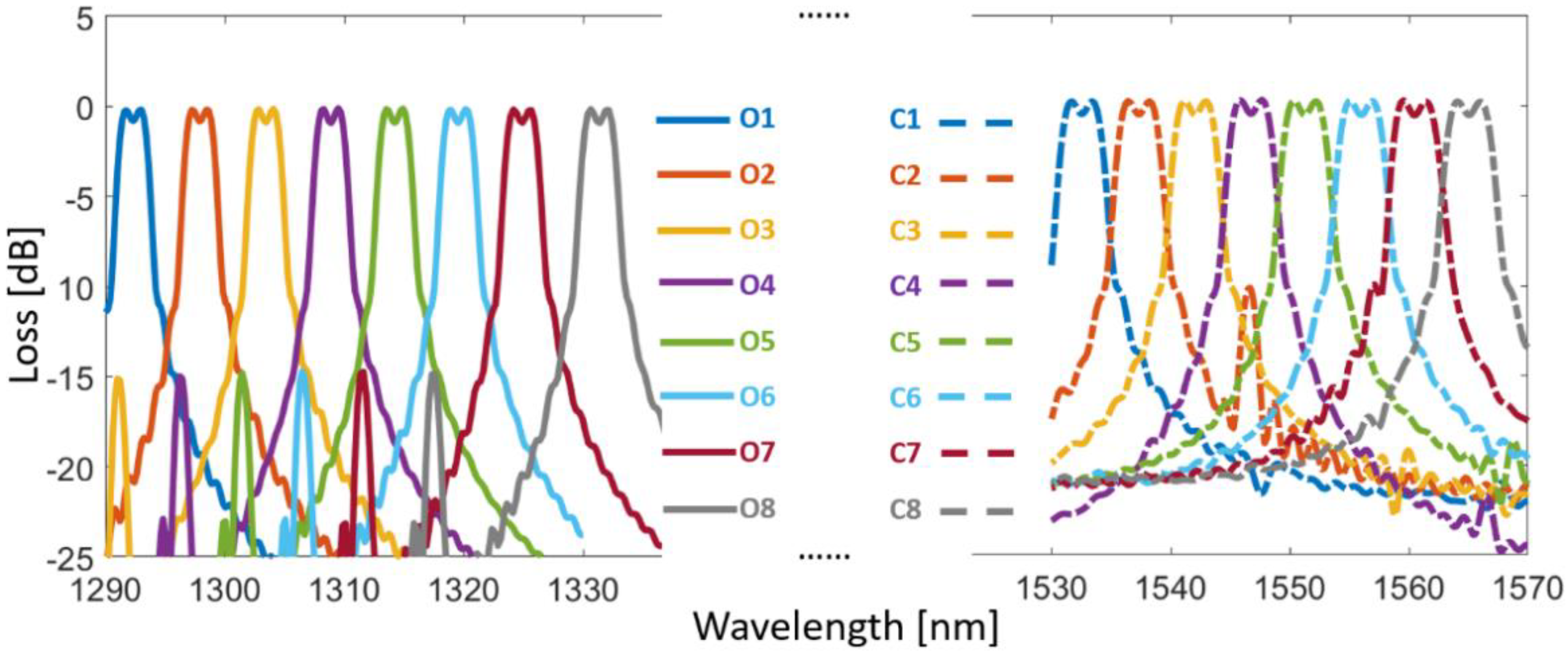
Table 2 illustrates the respective parameter settings of O-band and C-band. When the cycle changed by 1.5 nm, the wavelength shifted by 4nm. Using the above parameters, we simulated the 16-channel WDM of the O-band and C-band. The simulation results are shown in Figure 4.
Figure 4 shows the simulation results of designed 16-channel WDM. The wavelength demultiplexing of the channel was completed in the 1535–1565 nm bandwidth, and the loss was lower than 0.5 dB, with crosstalk less than 17 dB; The wavelength demultiplexing of the channel was completed in the 1290–1330 nm bandwidth, and the loss was lower than 0.5 dB, crosstalk less than 20 dB. It could be observed that in each channel, there was a slight decrease in loss before the center wavelength. This is caused by the reflection around the Bragg wavelength. To avoid possible crosstalk, we will tackle this problem in our next work.
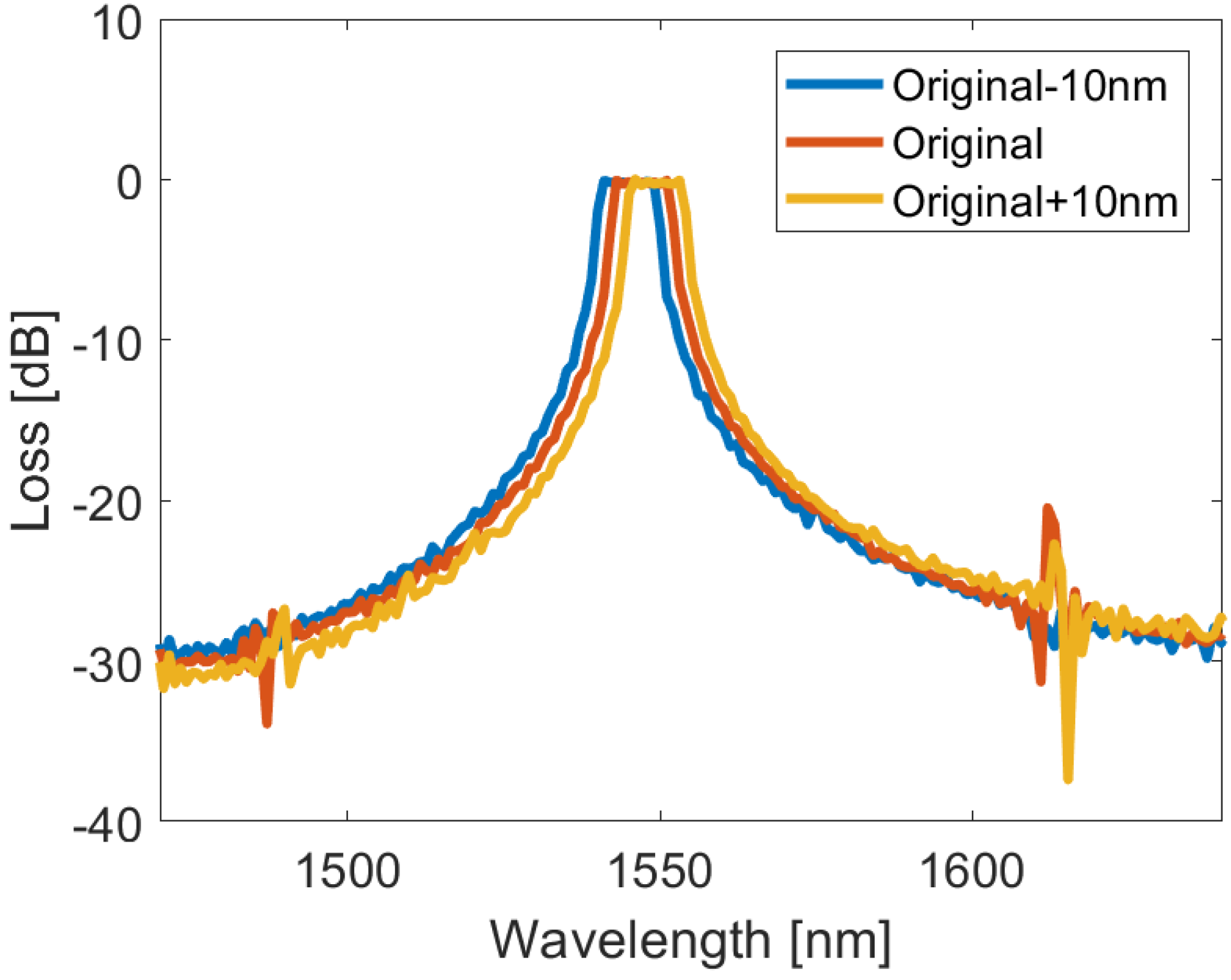
We also simulated fabrication-error-induced performance deterioration. Considering the structure was based on SWG perturbation and fabrication error usually takes on a different duty cycle value, the C4 duty cycles × period of 159.7 nm (original) and 159.7 ± 10 nm were simulated and compared, as shown in Figure 5. It can be seen in the figure that the fabrication error mainly resulted in a central wavelength shift while the cross-talk change was minor. The central wavelength was 1547 nm when the duty cycles × period was 159.7 nm, and the central wavelength shift was ~1 nm when the duty cycle × period changed from 159.7 − 10 nm to 159.7 + 10 nm. In other words, for 20 nm duty cycles × period device fabrication error, the central wavelength shift was ~1 nm. Moreover, as the structure was based on SWG perturbation, the duty cycle fabrication errors for each channel were similar in the same device. This indicates that the central wavelength shift caused by the fabrication error could be modified by an additional global temperature controller. For example, one could place the TiN layer above the WDM, utilizing elector-thermo effect to control the global temperature of the structure, and thus modify the center wavelength of the WDM.

4. Conclusions

In this work, we designed and simulated a 16-channel wavelength WDM based on SWG. Our design utilized an SWG perturbation structure to provide inverse couple condition for each channel, which could lower the transmission loss and enhance fabrication tolerance compared to a WDM on an SWG waveguide structure. Besides, with specific structure optimization, our design was capable of 16-channel WDM, covering both O-band and C-band. In our design, the loss and crosstalk of each channel was lower than 0.5 dB and 17 dB. When demultiplexing the O-band, the transmission loss of the C-band was lower than 0.05 dB. Our results imply that the proposed device is promising for broadband and low-loss wavelength demultiplexing with compact footprint and broad bandwidth.

Author Contributions

Conceptualization, Y.B.; data curation, Y.B. and L.Z.; formal analysis, Y.B. and L.W.; investigation, L.W. and L.Z.; methodology, Y.B. and L.W.; resources, L.W., P.W. and B.P.; software, Y.B., L.W. and L.Z.; supervision, P.W.; writing—original draft, Y.B.; writing—review & editing, L.W., P.W. and B.P. All authors have read and agreed to the published version of the manuscript.

Funding

This document is the results of the research project funded by Zhejiang Lab Research Funds (2022QA0AL01).

Institutional Review Board Statement

Not applicable.

Informed Consent Statement

Not applicable.

Data Availability Statement

Not applicable.

Conflicts of Interest

The authors declare no conflict of interest.

References

  1. Khalighi, M.A.; Uysal, M. Survey on free space optical communication: A communication theory perspective. IEEE Commun. Surv. Tutor. 2014, 16, 2231–2258. [Google Scholar]
  2. Gantz, J.; Reinsel, D.; Arend, C. The digital universe in 2020: Big data, bigger digital shadows, and biggest growth in the far east-western Europe. IDC Anal. Future 2012, 2007, 1–16. [Google Scholar]
  3. Thylén, L.; Wosinski, L. Integrated photonics in the 21st century. Photonics Res. 2014, 2, 75–81. [Google Scholar] [CrossRef]
  4. Xu, J.; Kong, M.W.; Lin, A.B.; Song, Y.H.; Yu, X.Y.; Qu, F.Z.; Han, J.; Deng, N. OFDM-based broadband underwater wireless optical communication system using a compact blue LED. Opt. Commun. 2016, 369, 100–105. [Google Scholar] [CrossRef]
  5. Amirabadi, M.A.; Kahaei, M.H.; Nezamalhosseni, S.A. Low complexity deep learning algorithms for compensating atmospheric turbulence in the free space optical communication system. IET Optoelectron. 2022, 16, 93–105. [Google Scholar] [CrossRef]
  6. Siew, S.Y.; Li, B.; Gao, F.; Zheng, H.Y.; Zhang, W.; Guo, P.; Xie, S.W.; Song, A.; Dong, B.; Luo, L.W.; et al. Review of Silicon Photonics Technology and Platform Development. J. Light. Technol. 2021, 39, 4374–4389. [Google Scholar] [CrossRef]
  7. Dong, P.; Chen, Y.-K.; Duan, G.-H.; Neilson, D.T. Silicon photonic devices and integrated circuits. Nanophotonics 2014, 3, 215–228. [Google Scholar] [CrossRef]
  8. Aydin, K. Nanostructured silicon success. Nat. Photonics 2015, 9, 353–355. [Google Scholar] [CrossRef]
  9. Bogaerts, W.; Chrostowski, L. Silicon Photonics Circuit Design: Methods, Tools and Challenges. Laser Photonics Rev. 2018, 12, 4374–4389. [Google Scholar]
  10. Shi, W.; Tian, Y.; Gervais, A. Scaling capacity of fiber-optic transmission systems via silicon photonics. Nanophotonics 2020, 9, 4629–4663. [Google Scholar]
  11. Brackett, C.A. Dense wavelength division multiplexing networks—Principles and applications. IEEE J. Sel. Areas Commun. 1990, 8, 948–964. [Google Scholar] [CrossRef]
  12. Piggott, A.Y.; Lu, J.; Lagoudakis, K.G.; Petykiewicz, J.; Babinec, T.M.; Vuckovic, J. Inverse design and demonstration of a compact and broadband on-chip wavelength demultiplexer. Nat. Photonics 2015, 9, 374. [Google Scholar] [CrossRef] [Green Version]
  13. Pan, P.; An, J.; Wang, Y.; Zhang, J.; Wang, L.; Qi, Y.; Han, Q.; Hu, X. Compact 4-channel AWGs for CWDM and LAN WDM in data center monolithic applications. Opt. Laser Technol. 2015, 75, 177–181. [Google Scholar] [CrossRef]
  14. Shi, W.; Yun, H.; Lin, C.; Greenberg, M.; Wang, X.; Wang, Y.; Fard, S.T.; Flueckiger, J.; Jaeger, N.A.F.; Chrostowski, L. Ultra-compact, flat-top demultiplexer using anti-reflection contra-directional couplers for CWDM networks on silicon. Opt. Express 2013, 21, 6733–6738. [Google Scholar] [CrossRef] [PubMed]
  15. Cheben, P.; Halir, R.; Schmid, J.H.; Atwater, H.A.; Smith, D.R. Subwavelength integrated photonics. Nature 2018, 560, 565–572. [Google Scholar] [CrossRef] [PubMed]
  16. Chen, J.Y.; Shi, Y.C. Flat-top CWDM (De) Multiplexers Based on Contra-Directional Couplers With Subwavelength Gratings. IEEE Photonics Technol. Lett. 2019, 31, 20032006. [Google Scholar] [CrossRef]
  17. Tao, S.; Huang, Q.; Zhu, L.; Liu, J.; Zhang, Y.; Huang, Y.; Wang, Y.; Xia, J. Athermal 4-channel (de-)multiplexer in silicon nitride fabricated at low temperature. Photonics Res. 2018, 6, 686–691. [Google Scholar] [CrossRef]
  18. Horst, F.; Green, W.M.; Assefa, S.; Shank, S.M.; Vlasov, Y.A.; Offrein, B.J. Cascaded Mach-Zehnder wavelength filters in silicon photonics for low loss and flat pass-band WDM (de-)multiplexing. Opt. Express 2013, 21, 11652–11658. [Google Scholar] [CrossRef] [PubMed]
  19. Huang, Q.; Yu, J. Coherent interaction between two orthogonal travelling-wave modes in a microdonut resonator for filtering and buffering applications. Opt. Express 2014, 22, 25171–25182. [Google Scholar] [CrossRef]
  20. Chang, L.; Xie, W.; Shu, H.; Yang, Q.F.; Shen, B.; Boes, A.; Peters, J.D.; Jin, W.; Xiang, C.; Liu, S.; et al. Ultra-efficient frequency comb generation in AlGaAs-on-insulator microresonators. Nat. Commun. 2020, 11, 1331. [Google Scholar] [CrossRef] [Green Version]
  21. Rakhshani, M.R.; Mansouri-Birjandi, M.A. Heterostructure four channel wavelength demultiplexer using square photonic crystals ring resonators. J. Electromagn. Waves Appl. 2012, 26, 17001707. [Google Scholar] [CrossRef]
  22. St-Yves, J.; Bahrami, H.; Jean, P.; LaRochelle, S.; Shi, W.J.O.l. Widely bandwidth-tunable silicon filter with an unlimited free-spectral range. Opt. Lett. 2015, 40, 5471–5474. [Google Scholar] [CrossRef] [PubMed] [Green Version]
  23. Li, C.; Zhang, M.; Xu, H.; Tan, Y.; Shi, Y.; Dai, D. Subwavelength silicon photonics for on-chip mode-manipulation. PhotoniX 2021, 2, 11. [Google Scholar] [CrossRef]
  24. Sun, L.; Zhang, Y.; He, Y.; Wang, H.W.; Su, Y.K. Subwavelength structured silicon waveguides and photonic devices. Nanophotonics 2020, 9, 1321–1340. [Google Scholar] [CrossRef]
  25. Wang, F.; Xu, X.; Zhang, C.; Sun, C.; Zhao, J. Design and Demonstration of Compact and Broadband Wavelength Demultiplexer Based on Subwavelength Grating (SWG). IEEE Photonics J. 2022, 14, 6621606. [Google Scholar] [CrossRef]
  26. Mohammed, Z.; Paredes, B.; Rasras, M. A CMOS Compatible On-chip MMI based Wavelength Diplexer with 60 Gbit/s System Demonstration. In Proceedings of the Optical Fiber Communication Conference, San Diego, CA, USA, 6–10 March 2022; p. M4J. 3. [Google Scholar]
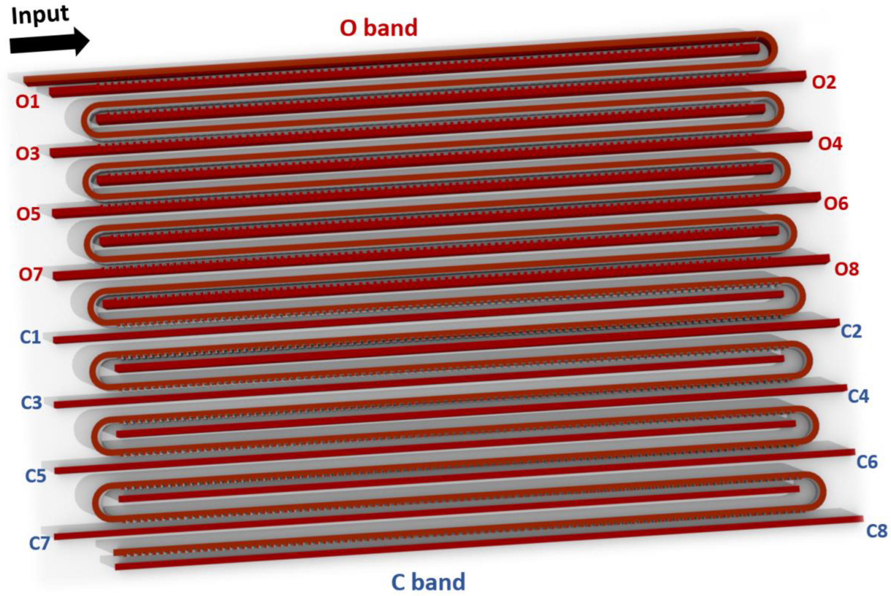
Figure 1. Single-channel grating structure diagram. Broad-spectrum light is input from the input port, the light is transmitted along the main waveguide, and is coupled to the output waveguide at a position that satisfies the wave vector matching condition.
Applsci 13 01833 g001
Figure 2. (a) Structure of a single reverse−coupled SWG wavelength division device. (b) Variation of effective refractive index with width for 220 nm thick strip waveguides in O−band and C−band. (c) Optical field map of the grating with a central wavelength of 1550 nm. (d) Losses at the through and output ends of the 1550 nm center wavelength grating.
Applsci 13 01833 g002
Figure 3. (a) The loss of WDM SWG in O−band with different parameters when transmitting C−band. (b) O−band coupling light field diagram. The light field map of the C-band (almost lossless output from the through to the end) when WDM is performed in the O−band.
Applsci 13 01833 g003
Figure 4. The WDM simulation results of 16 channels in the O-band and C-band, the loss of the O-band is lower than 0.5 dB, crosstalk below 20 dB, C-band loss lower than 0.5 dB, crosstalk below 17 dB.
Applsci 13 01833 g004
Figure 5. Fabrication error induced central wavelength shift for C4.
Applsci 13 01833 g005
Table 1. O-band and C-band central wavelength SWG parameters.
Wb
(nm)
Ws
(nm)
Wa
(nm)
Gap
(nm)
Pitch
(nm)
Duty
Cycle
N
1310 nm6503501006502340.5855
1550 nm6004001007003210.5623
Table 2. O- and C-band wave decomposition multiplexing parameters.
Δλ (nm)Δpitch (nm)Loss (dB)CT (dB)Band (nm)
O-band51.50.52045
C-band51.50.51740
Disclaimer/Publisher’s Note: The statements, opinions and data contained in all publications are solely those of the individual author(s) and contributor(s) and not of MDPI and/or the editor(s). MDPI and/or the editor(s) disclaim responsibility for any injury to people or property resulting from any ideas, methods, instructions or products referred to in the content.