Abstract
This article introduces a process to design, simulate, and measure a novel multi-band patch antenna with different operation modes, i.e., band centers and bandwidths. Switching between operation modes is possible using a pair of PIN diodes to connect different parts of the antenna with the main antenna patch. Such a reconfigurable design allows for individual control of each frequency range. The main operation mode of the resulting antenna has an impedance bandwidth with two bands, one from 2.4 GHz to 2.73 GHz and another from 3.4 GHz to 5.73 GHz, with a maximum gain of 4.85 dBi and stable radiation patterns. The resulting antenna is suitable for applications using both ultra-wideband technologies and wireless local-area network (WLAN) technologies.
1. Introduction
Patch antennas (PAs) consist of a thin metal patch placed over a ground plane, with a feed point connected to a transmission line. They are directional antennas and can operate at different frequencies based on their size and shape.
Over the last few years, they have become increasingly popular due to their small size, low profile, and ease of integration with other electronic components [1,2], compared to traditional antennas. Their small size, high gain, and robustness are features that are highly valued in the fields of mobile device fabrication and wireless communication systems, where they are widely used. There is ongoing research to design compact and efficient PAs that are capable of supporting high-speed data transmission so they can be included in micro-electromechanical systems (MEMS) that can be integrated into small devices [3,4,5,6,7,8]. In recent years, advances in material technology and manufacturing techniques have led to the production of patch antennas with even smaller dimensions and higher performance [9,10,11,12,13]. The quest for further reduction in PA sizes remains a research field with open challenges, where new miniaturization techniques are under development [14,15,16,17].
In wireless communication systems, there are two common types of antennas: ultra-wideband (UWB) and multi-band antennas [18,19,20,21]. While both of them are designed to cover a wide range of frequencies, they differ in their features and applications. Multi-band antennas consist of several resonating elements; each tuned to a different frequency band, and designed to operate across multiple narrow frequency bands. Multi-band antennas are suitable for applications that require communication over multiple frequencies, such as cellular networks and Wi-Fi systems. On the other hand, UWB antennas are designed to cover a wide spectrum using a single resonant element [22,23,24,25]. They operate over a broad frequency range without the need for multiple resonators.
In this context, reconfigurable planar antennas have become increasingly popular due to their ability to switch between different modes of operation, frequencies, and radiation patterns, combining characteristics of both multi-band and UWB antennas. They are commonly used in modern wireless communication systems that require a wide range of frequencies, such as ultra-wideband (UWB) [26,27,28] and wireless local area network (WLAN) applications. In recent times, a few approaches have been reported in the literature to achieve UWB characteristics: tree-like fractal slots [29], compact folded network antennas [30], reconfigurable antennas using diodes on an FR4 substrate [31,32,33], fractal arrays [34], and MIMO (multiple-input multiple-output) antennas [35,36]. The use of reconfigurable components, such as PIN diodes, as in ref. [33], allows the antenna to switch between different frequency bands, enabling it to adapt to different communication requirements. The design of this type of antenna is challenging and requires the use of electromagnetic simulations and optimization techniques to achieve the desired performance.
In this paper, we present a rounded rectangular reconfigurable patch antenna that can support both the UWB application and the WLAN band, where the reconfigurability is achieved by using PIN diodes to switch between different resonant modes. It incorporates one notch band to create a band for the UWB frequency bands and two additional resonant elements to create a band operation for the WLAN frequency bands, with a hybrid shape slot composed of a circle and a rectangle. The hybrid-shaped design reduces the overall size of the antenna while maintaining a satisfactory level of performance in terms of bandwidth and radiation efficiency. The circular shape provides transverse radiation patterns, whereas the rectangular shape helps reduce cross-polarization.
This article is structured into four sections. In Section 2, the proposed antenna’s design geometry and its various development stages are explained. The impacts of the activation states of the PIN diodes and the gap length on the antenna’s overall performance are also analyzed. In Section 3, we present both simulated and measured results, focusing on the antenna’s reflection coefficient and radiation properties. The performance of our proposed antenna is compared with previously published works from recent years. The conclusions are presented in Section 4.
2. Materials and Methods
2.1. Proposed Design
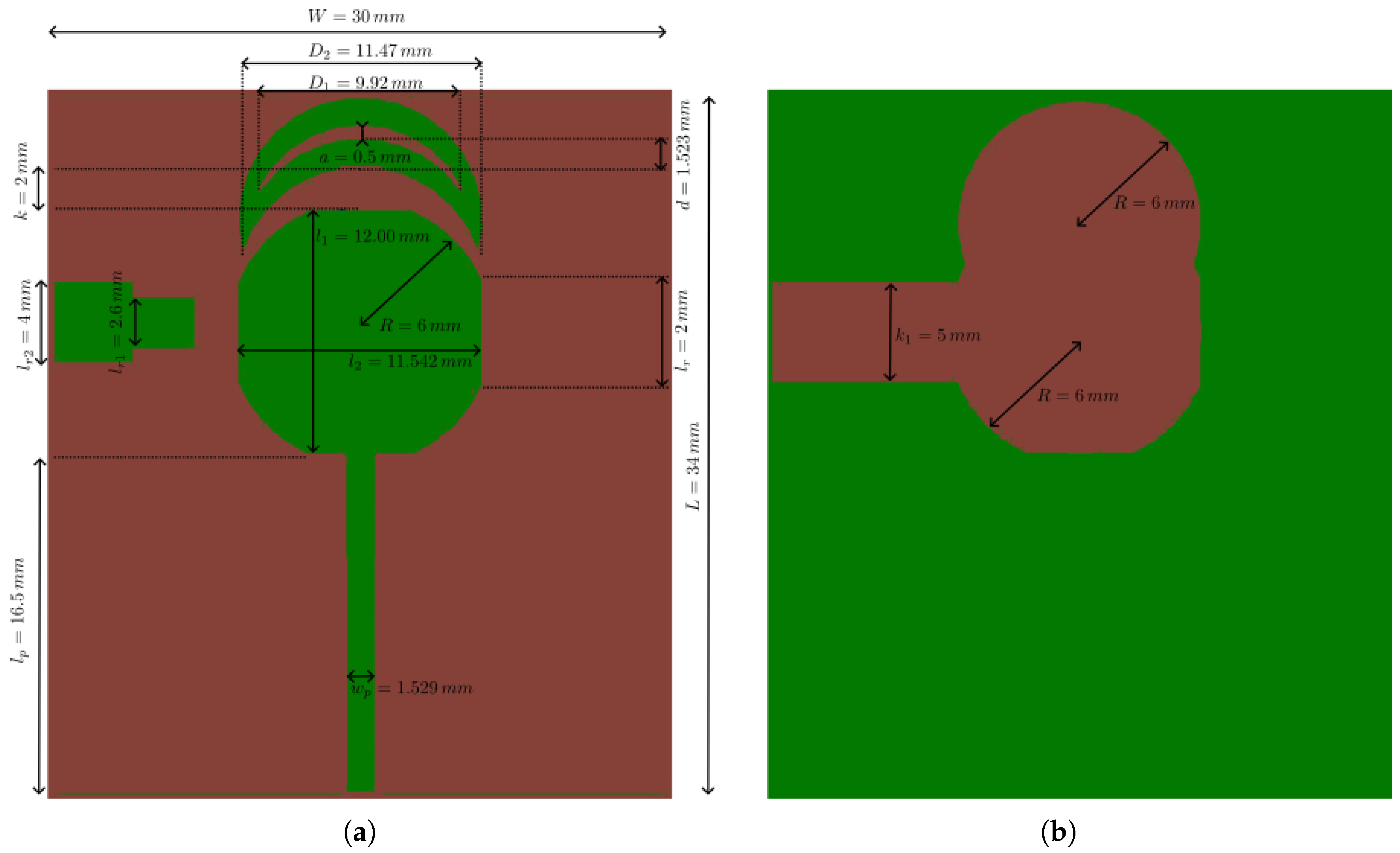
The antenna design (Figure 1) consists of a rectangular monopole of size mm2 that is constructed on an FR4 substrate with a relative permittivity of and a thickness of mm. This monopole acts as the primary radiator for the antenna. A rounded rectangular patch (main patch (MP)) is placed on this rectangular monopole. The MP is the result of the intersection of a circle of radius R and a rectangle centered on the circle, with sides 12 mm and mm. The main patch (MP) is fed with a microstrip line with length mm and width mm, and is connected to two other smaller patches through two rectangular slots where PIN diodes have been placed: a semicircular patch (SCP) and a rectangular patch (RP). A summary of the dimensions of the antenna is shown in Table 1. The arrangement and shapes of the patches have been designed to produce the necessary resonance frequency, radiation pattern, input impedance, and bandwidth. The patch antenna includes a hybrid-shaped slot in the ground plane. The shape of the slot is equal to the envelope of the projection of the MP, the SCP, and the RP on the ground plane. The addition of this slot provides the antenna with a large bandwidth and allows for the control of the radiation characteristics of the antenna.
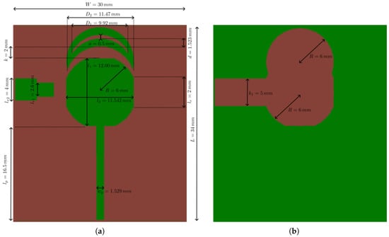
Figure 1.
Shape and dimensions of the proposed patch antenna (PA). (a) Front side of the PA antenna. (b) Back side of the PA antenna.

Table 1.
Dimensions in mm of the proposed antenna.
2.2. Development Stages
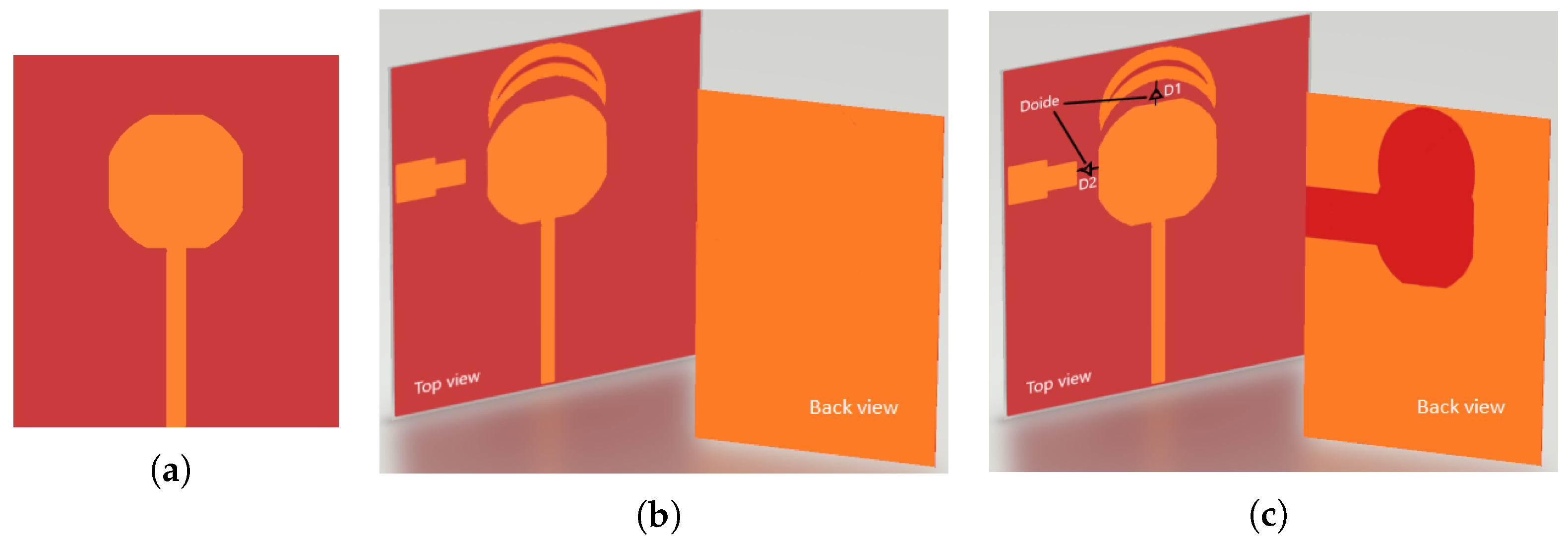
Three iterations are needed to reach the final design of the antenna. They are shown in Figure 2. The changes that were introduced at each stage were chosen to reach the target reflection coefficient with a UWB and a WLAN band. The simulations were conducted using the Ansys© Electronics Desktop 2019 R3-High-Frequency Structure Simulator on a laptop equipped with an Intel Core i7-4710MQ CPU running at GHz and 8 GB of RAM.

Figure 2.
Different developmental stages of the proposed antenna design. (a) First iteration. (b) Second iteration. (c) Proposed design.
The initial iteration (Figure 2a) was a simple rounded rectangular patch antenna with a microstrip line feed. The radius (R) of the MP was calculated from the initiating patch frequency (F) in the following way [37,38]:
where is the relative permittivity, h is the thickness of the substrate in cm, and is the resonant frequency of the patch antenna in Hz.
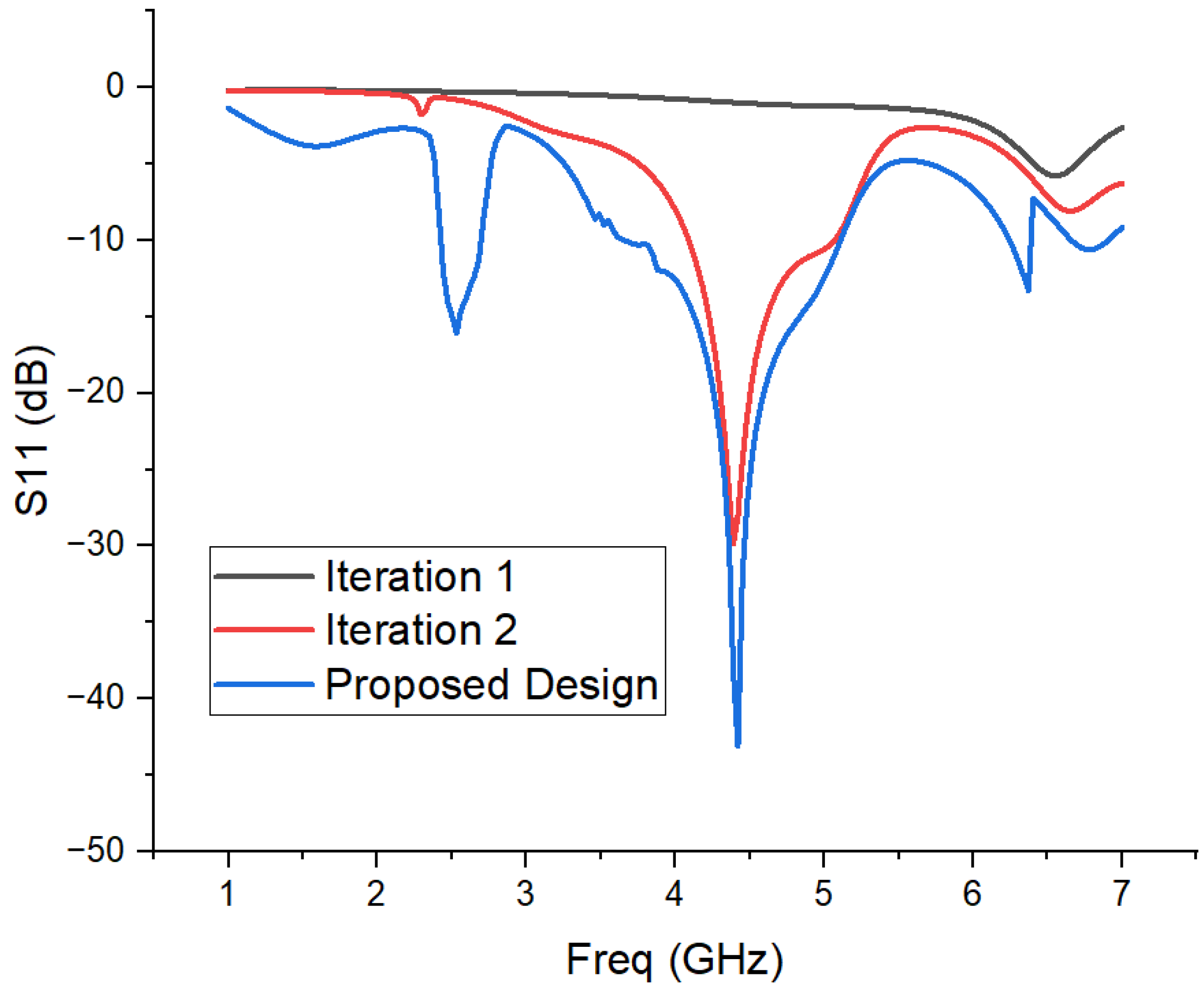
This first design does not have a band and shows a constant reflection coefficient (Figure 3, Iteration 1).

Figure 3.
Proposed antenna reflection coefficients for different development stages.
For the second iteration (Figure 2b), the antenna was modified by adding the SCP and the RP with semicircular slots, including two rectangular slots placed strategically to improve the impedance matching and increase the operating bandwidth. In this iteration, the performance, considering the desired operating bands, was significantly improved. This design has a bandwidth of GHz with a return loss up to dB. The new shape enables the wideband operation from 3.87 GHz to 4.68GHz (Figure 3, Iteration 2). However, the antenna still does not meet the requirements of the bands.
To further improve the antenna matching and widen the operating band to cover the band requirements, the patch is further modified (Figure 2c). A rounded rectangular patch is placed with a single feed, which is connected to the rectangular and semicircular patches with two rectangular slots. The semicircular and rectangular patches are positioned at the ground plane layer in parallel to the rounded rectangle patch as a slot. This iteration gives the desired UWB and WLAN bands with an increased operating bandwidth to cover frequency bands for planned wireless communication applications. In the simulation of this iteration, the antenna has—in the WLAN band—a low-UWB characteristic that covers the frequency bands (2.3–2.6 and 3.7–5.4 GHz); the two resonance frequencies are at GHz and GHz, with a return loss of dB and dB, respectively, and a gain that exceeds dB (Figure 3, Proposed Design).
2.3. Equivalent Circuit Model of Pin Diode
A PIN diode can be used as a switch to modify the electrical length of the antenna, influencing its resonant frequency and radiation pattern. Two diodes (BAP65−02 were used in our configuration [39], which can be modeled as a series or parallel combination of passive components (Figure 4), to achieve the desired reconfiguration of the patch antenna. When the DC bias voltage is above a certain threshold, the PIN diode can be modeled as a serial combination of resistance and inductance . When the DC bias voltage is below the activation threshold, the diode can be modeled as a parallel combination of capacitor and resistor in series with inductance.
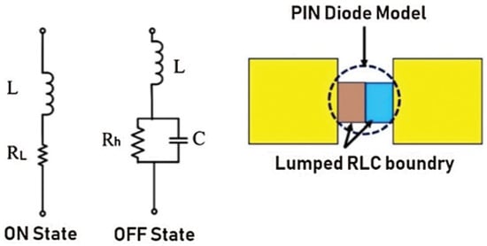
Figure 4.
Equivalent circuit model of the PIN diode.
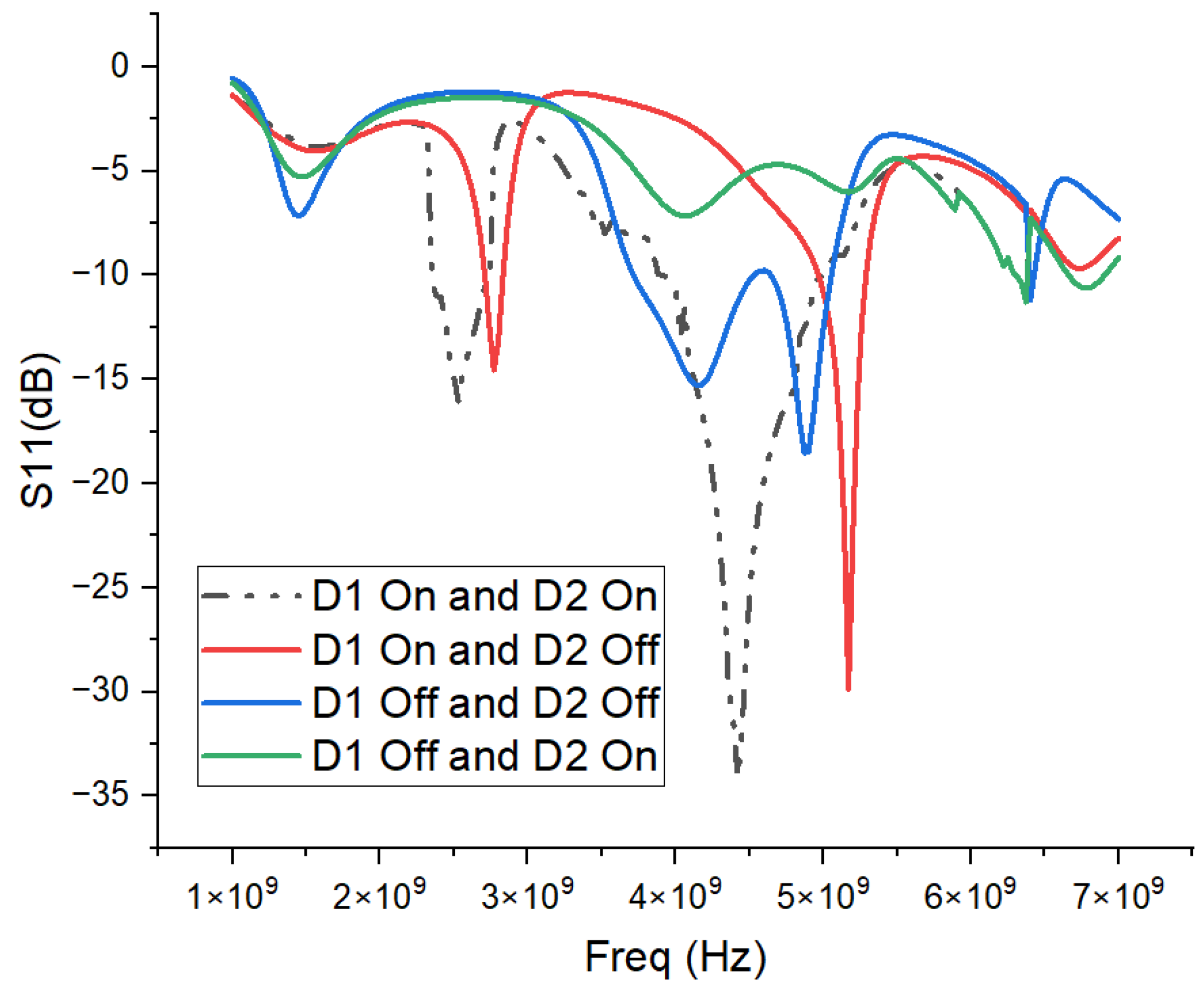
Figure 5 shows the comparison of parameters between the various operating modes providing the switching states of the PIN diodes. The study found that two of the four ON–OFF state combinations of the PIN diodes provided a bi-band, i.e., the antenna operated at two resonance frequencies.
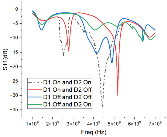
Figure 5.
Reflection coefficients of the proposed antenna for the different states of two PIN diodes.
- When the two PIN diodes are on, the two resonance frequencies are at GHz and GHz, with a return loss of dB and dB, respectively.
- When diode D1 is turned on and diode D2 is off, the two resonance frequencies are at GHz and GHz, with a return loss of dB and dB, respectively.
- When diode D1 is switched off and diode D2 is on, there is only one wide bandwidth of GHz impedance.
- When both diodes are turned off, the antenna does not have a band.
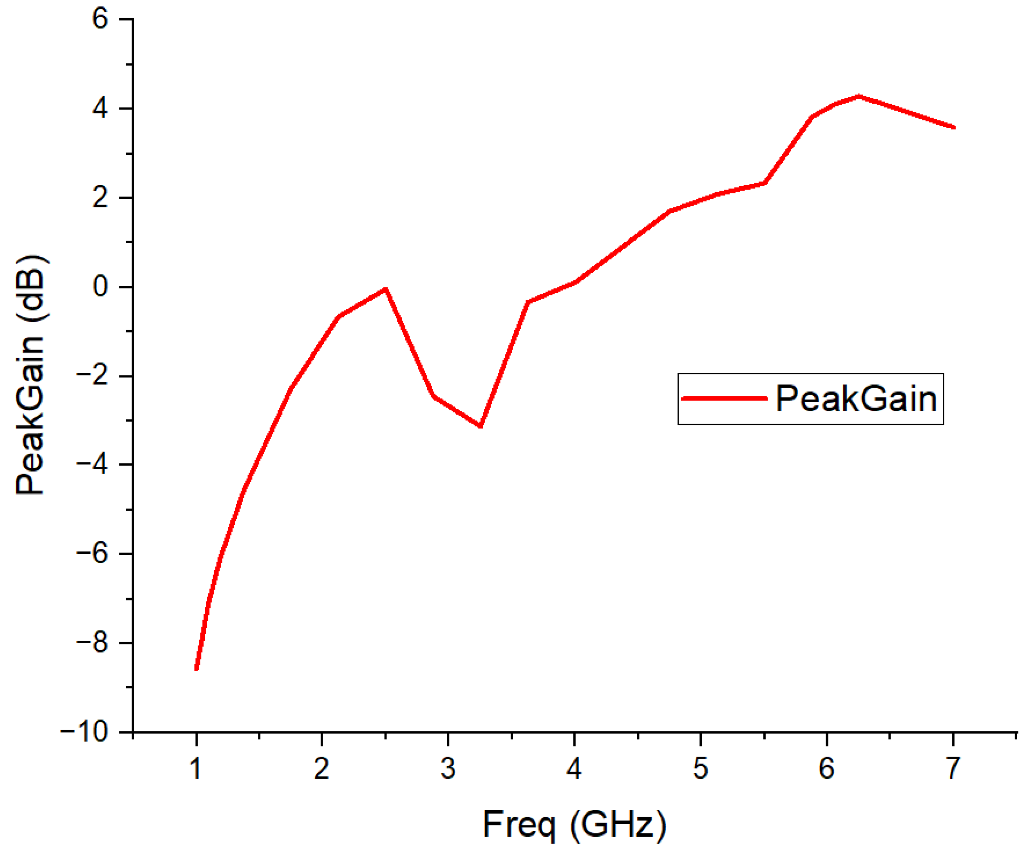
In general, the study shows that the proposed antenna with two PIN diodes has multiple operating states, which can be used to achieve different frequency bands and bandwidths. Figure 6 shows the proposed antenna peak gain for the configuration with both diodes switched on as a function of frequency. As can be observed, as the frequency increases, the peak gain also increases. This could be explained by the fact that the size of the patch becomes larger than its wavelength when the frequency increases to dB. However, the increase in gain is limited by the antenna’s efficiency and losses, including radiation losses and conductor losses. At higher frequencies, the conductor losses due to the skin effect become more significant, leading to a decrease in efficiency and gain. This is why the gain of the antenna starts to decrease at higher frequencies, as seen in Figure 6. Additionally, at very high frequencies, the antenna’s ability to efficiently capture or radiate the signal becomes more difficult due to limitations in the antenna design and size.

Figure 6.
Peak gain of the suggested patch when both diodes are turned on.
2.4. Parametric Study
The value of the gap length ( in Figure 1) in the ground plane of the patch antenna directly affects the reflection coefficient, . A parameter sweep from 3 mm to 7 mm in steps of 1 mm was performed to find the best value, considering the design goals. Figure 7 shows the results for different gap lengths on the antenna configuration with both diodes on. At 5 mm, the antenna has a reflection coefficient with a WLAN and a low-UWB band with the largest bandwidth.
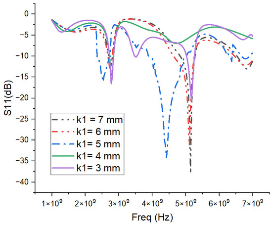
Figure 7.
Reflection coefficients of the proposed antenna for the different values of parameter .
For values of decreasing and increasing away from = 5 mm, the position and bandwidth of the bands change. In both cases, the notch band is shifted to larger frequencies, and the bandwidth of both bands of the antenna decrease. The impedance of the antenna is sensitive to the length of the gap, and changing its value leads to a mismatch in the impedance of the antenna.
Overall, the numerical experiment shows that the gap length in the ground plane of the antenna design can have a significant impact on its frequency response and bandwidth. Designers must carefully optimize the gap length to achieve the desired performance characteristics of the antenna.
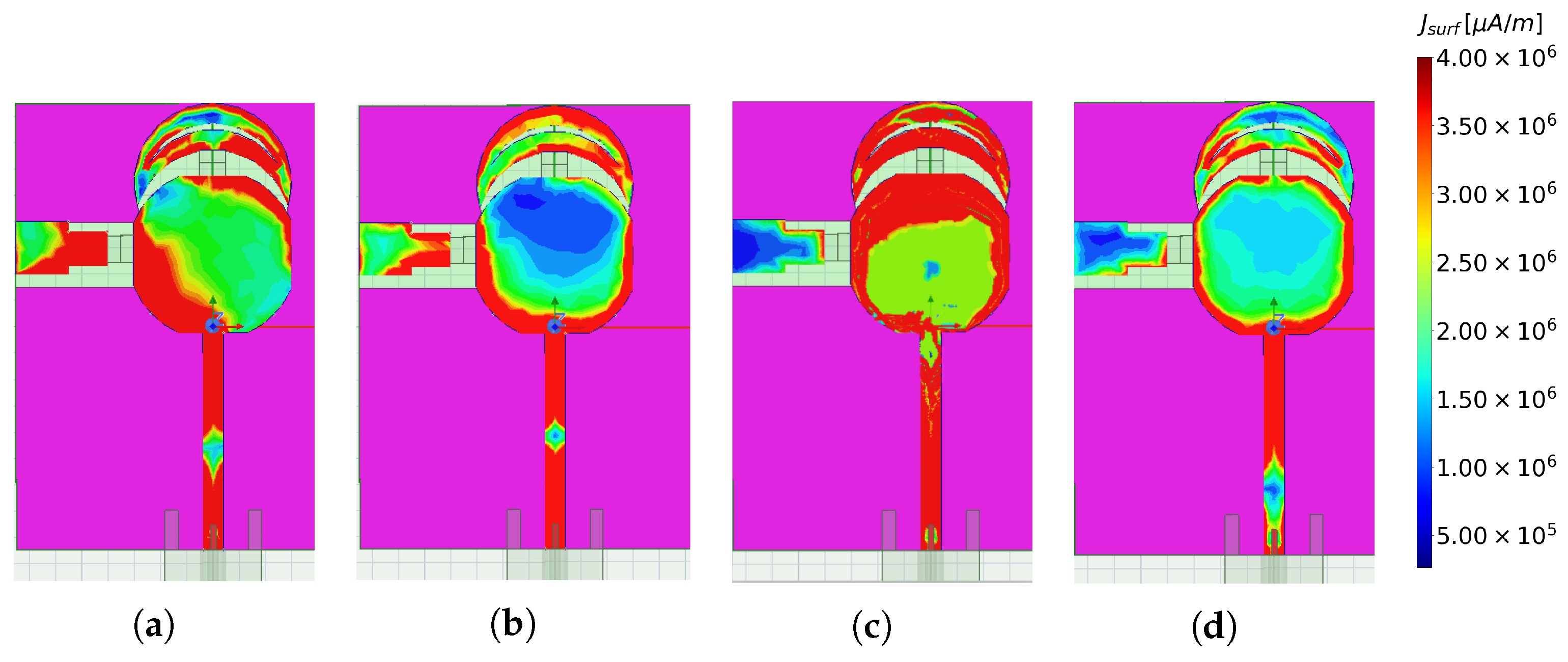
2.5. Surface Current Distribution
Figure 8 illustrates the dependence of the surface current distribution on the different switching states of two PIN diodes at a working frequency of 4 GHz. In the case where both PIN diodes are on (Figure 8a), the study observed that most of the surface current spreads from the bottom of the patch toward the middle of the main patch, as well as to the semicircular and rectangular patches. When the left diode is on while the right diode is off (Figure 8b), the surface current mainly extends from the bottom to the middle and the edge of the main patch. Additionally, it propagates toward the left side of the left diode in the rectangular patch. Conversely, when the left diode is off and the right diode is on (Figure 8c), the surface current distribution exhibits an opposite pattern. It primarily extends from the bottom to the middle and the edge of the main patch while propagating toward the right side of the right diode in the semicircular patch. Finally, when both PIN diodes are off (Figure 8d), the surface current spreads from the bottom to the edges of the two PIN diodes in the main patch.
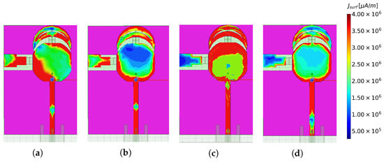
Figure 8.
Surface current distribution of the proposed antenna design at a frequency of 4 GHz. (a) Both PIN diodes are on. (b) Left diode is on the right is off. (c) Left diode is off and the right is on. (d) Both PIN diodes are off.
3. Experimental Results and Discussion
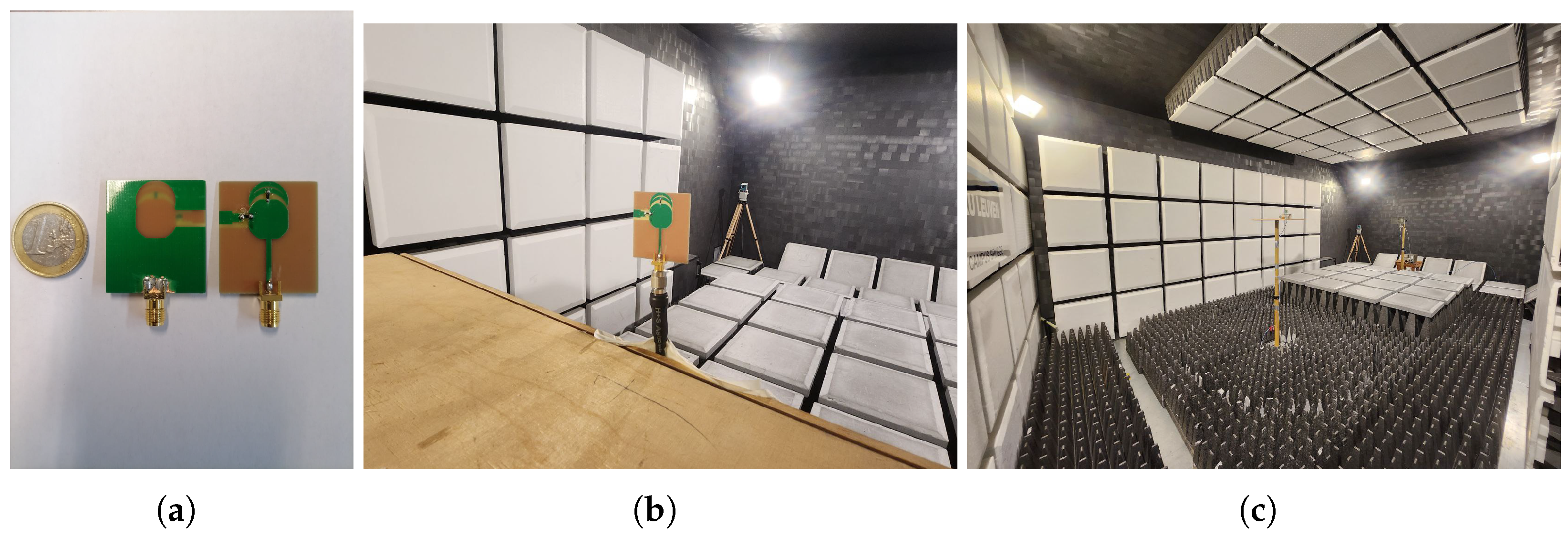
We fabricated and measured a hardware prototype to validate the simulation results and check the actual antenna behavior. In this case, a commercially available substrate was used to fabricate the proposed PA (shown in Figure 9a), which was then measured using a vector network analyzer (VNA) and an anechoic chamber to determine its return loss. The anechoic chamber and the antenna under measurement can be seen in Figure 9b,c. Additionally, to measure the far-field parameters of the antenna, such as its radiation pattern, an electromagnetically isolated RF anechoic chamber was used. By measuring the radiation pattern in the anechoic chamber, the antenna’s performance can be characterized, and any deviations from the simulation results can be identified and analyzed.

Figure 9.
(a) Fabricated prototype. (b) Antenna under test. (c) Measurement of the far-field parameters in facilities at KU Leuven.
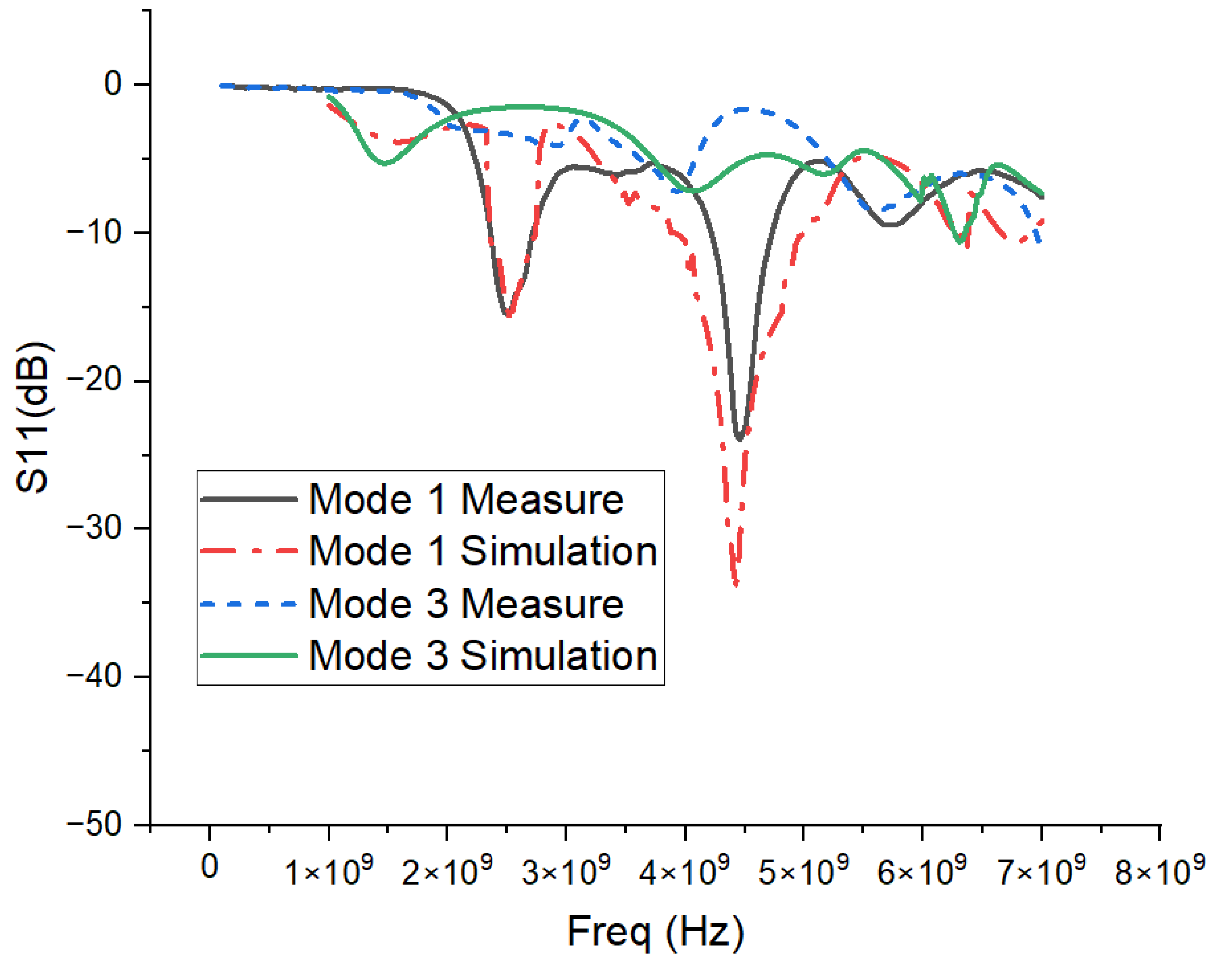
The reflection coefficient of the antenna was measured for its different operation states. Figure 10 shows the results of the measurements compared to the simulations performed for two of the operation states: when both diodes are on (and the antenna shows two operations bands) and when diode D1 is off, and diode D2 is on (and there is a wide band around GHz). When both diodes are active, the fabricated antenna covers both the WLAN and low-ultra-wideband spectrum in the ranges of 2.4–2.5 GHz and 4.1–5.1 GHz, respectively. The simulation and the measurements agree very well on the positions of the bands and approximately well on the widths of the bands. When diode D1 is off, both measurements and simulations yield a featureless reflection coefficient with no bands, even if the particular shape of differs. The absence of features is due to the change in the electrical size of the antenna caused by the operation states of the diodes. When PIN diode D1 is off and PIN diode D2 is on, the semicircular patch is disconnected and the rectangular part is connected, respectively. In this configuration, the electrical length of the antenna is such that the resonances are outside the frequency range covered in Figure 10.
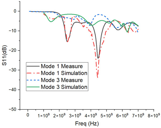
Figure 10.
Comparison of measured and simulated reflection coefficient of the proposed PA.
The simulated and measured reflection coefficients of the antenna are in good agreement for both frequency bands, further validating the accuracy of the simulation process used to model the antenna’s behavior. The antenna design process can be reliably modeled using simulation tools.
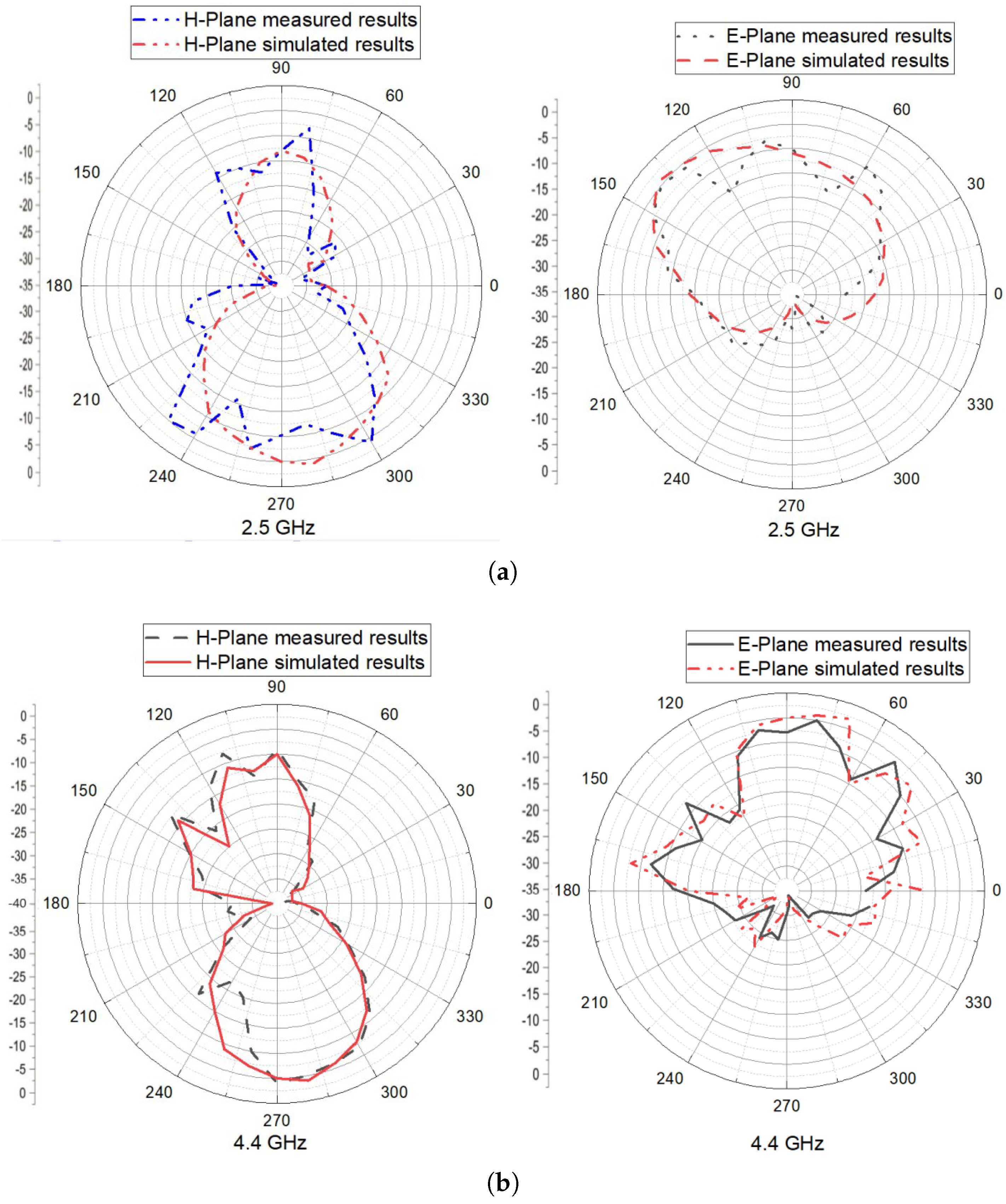
Figure 11 illustrates the simulated and measured 2D radiation patterns in the E- and H-planes for the proposed antenna. The E-plane (or azimuth) represents the radiation in the plane perpendicular to the antenna’s feeding mechanism. It shows how the antenna radiates energy in the horizontal plane around the antenna. The H-plane (or elevation) represents the radiation in the plane containing the antenna’s feeding mechanism. It shows how the antenna radiates energy in the vertical plane, typically above or below the antenna. The results show strong agreement between the simulation and the measurements, indicating the accuracy of the antenna design. The antenna provides relatively stable radiation patterns at all resonating frequencies, ensuring its wideband operation. In the H-plane, the antenna offers a nearly omnidirectional radiation pattern at the first resonant frequency and a quasi-omnidirectional radiation pattern at higher frequencies, ensuring coverage over a broad range of frequencies. In contrast, in the E-plane, the radiation pattern is bidirectional at the first resonant frequency ( GHz) and quasi-omnidirectional at the higher frequency ( GHz), as shown in Figure 10. Changes in the radiation pattern at high frequencies can be attributed to the influence of the high frequencies on the FR-4 substrate used in the antenna. Overall, the results demonstrate that the proposed antenna is well-suited for WLAN and low-UWB applications, providing stable and wideband radiation patterns in both E and H planes.
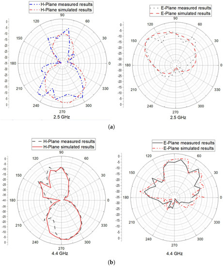
Figure 11.
Comparison of the measured and simulated 2D radiation patterns of the proposed PA. (a) Radiation patterns at a frequency of GHz. (b) Radiation patterns at a frequency of GHz.
Comparison with the State-of-the-Art WLAN and UWB Antennas
The proposed antenna has a large bandwidth range of up to GHz (2.35–2.74 GHz) and a reflection coefficient value of dB. In addition, it has a compact design, and it offers a better impedance bandwidth and gain when compared to the other works. Other antennas in the literature do not exceed GHz in the band, as reported in [18,40]. The antenna proposed in [41] presents a frequency response with an impedance bandwidth ranging from 2.4 GHz to 2.485 GHz. However, the antenna proposed in this paper still outperforms this result in terms of bandwidth range. Table 2 presents a comparison of our proposed antenna’s performance with previously published works from recent years. The table highlights various measured parameters, such as the frequency responses and the impedance bandwidth ranges of the reflection coefficient, and the size of the patch antenna.
Table 2.
Comparison with other antennas reported in the literature.
From the table, it is evident that the proposed antenna outperforms all other comparative literature works in terms of its compact size, better impedance bandwidth, and reflection coefficient.
4. Conclusions
The presented work proposes a reconfigurable patch antenna for WLAN and low-UWB bands, boasting a compact design, high gain, and a stable radiation pattern. The proposed antenna has a simple geometry composed of three patches connected by two positioned PIN diodes. Activating these diodes provides different modes of operation. This design achieves bandwidth ranges from 2.35 GHz to 2.74 GHz and 3.88 GHz to 5.1 GHz, which are relevant for mobile communication applications. Additionally, an extra stub was loaded to ensure WLAN band capability.
The validation measurements, taken from a fabricated prototype, matched the simulation results, indicating the effectiveness of the design. The compact dimensions of the antenna make it suitable for use in portable devices, such as smartphones and tablets, which require a small form factor antenna for wireless communication. The proposed antenna’s robustness and high gain enable it to maintain a stable connection, even in low-signal areas.
Overall, the presented work offers a novel solution for designing compact and efficient antennas for WLAN and low-UWB bands, addressing the challenges of mobile communication. The proposed design can serve as a basis for further research in the field of compact antenna design for wireless communication.
Author Contributions
Conceptualization, M.B.; project administration, S.B.; software, M.B., A.M.M. and F.A.; supervision, S.B.; validation, M.B., A.M.M. and M.G.-A.; writing—original draft, M.B.; writing—review and editing, S.B. and A.G.B. All authors have read and agreed to the published version of the manuscript.
Funding
This paper was published under the project eSAFE-UAV PID2019-106120RB-C32 funded by MCIN/AEI/10.13039/501100011033. Miriam Gonzalez Atienza received funding from the European Union’s Horizon 2020 research and innovation program under Marie Skłodowska-Curie grant agreement no. 955816. The project website is https://eternity-project.eu/ (last accessed on 1 August 2023). This publication reflects only the author’s view, exempting the European Union from any liability. Farah Amador’s work is funded by a SCHLUMBERGER FOUNDATION award https://www.facultyforthefuture.net/.
Institutional Review Board Statement
Not applicable.
Informed Consent Statement
Not applicable.
Data Availability Statement
Not applicable.
Acknowledgments
The authors wish to thank the laboratory of the M-group (FMEC) at KU Leuven Campus Bruges for providing us with the facilities to obtain the experimental data shown in this paper, namely to the test engineer at FMEC Klaas Pluvier for assisting in the measurements performed.
Conflicts of Interest
The authors declare no conflict of interest.
References
- Zhang, X.; Xu, H.; Xie, Y.; Wu, Q. A dual band-notched antenna for UWB applications. Prog. Electromagn. Res. Lett. 2021, 96, 105–111. [Google Scholar] [CrossRef]
- Andrews, J.G.; Buzzi, S.; Choi, W.; Hanly, S.V.; Lozano, A.; Soong, A.C.; Zhang, J.C. What will 5G be? IEEE J. Sel. Areas Commun. 2014, 32, 1065–1082. [Google Scholar] [CrossRef]
- Derneryd, A. A theoretical investigation of the rectangular microstrip antenna element. IEEE Trans. Antennas Propag. 1978, 26, 532–535. [Google Scholar] [CrossRef]
- Kara, M. Closed-form expressions for the resonant frequency of rectangular microstrip antenna elements with thick substrates. Microw. Opt. Technol. Lett. 1996, 12, 131–136. [Google Scholar] [CrossRef]
- James, J.R.; Hall, P.S. Handbook of Microstrip Antennas; IET: London, UK, 1989; Volume 1. [Google Scholar]
- Johari, S.; Jalil, M.A.; Ibrahim, S.I.; Mohammad, M.N.; Hassan, N. 28 GHz microstrip patch antennas for future 5G. J. Eng. Sci. Res. 2018, 2, 1–6. [Google Scholar]
- Mungur, D.; Duraikannan, S. Microstrip patch antenna at 28 GHz for 5G applications. J. Sci. Technol. Eng.-Manag.-Adv. Res. Innov. 2018, 1, 20–22. [Google Scholar]
- Kenane, E.; Bakhti, H.; Bentoumi, M.; Djahli, F. A Dynamic Invasive Weeds Optimization Applied to Null Control of Linear Antenna Arrays with Constrained DRR. Adv. Electromagn. 2021, 10, 52–61. [Google Scholar] [CrossRef]
- Bikrat, M.; Bri, S. Multiband Reconfigurable Planar Antenna for Wireless Mobile Communications. In Proceedings of the International Conference on Digital Technologies and Applications, Fez, Morocco, 27–28 January 2023; Springer: Berlin/Heidelberg, Germany, 2023; pp. 279–288. [Google Scholar]
- Deffenbaugh, P.I.; Rumpf, R.C.; Church, K.H. Broadband microwave frequency characterization of 3-D printed materials. IEEE Trans. Compon. Packag. Manuf. Technol. 2013, 3, 2147–2155. [Google Scholar] [CrossRef]
- Liang, M.; Shemelya, C.; MacDonald, E.; Wicker, R.; Xin, H. 3-D printed microwave patch antenna via fused deposition method and ultrasonic wire mesh embedding technique. IEEE Antennas Wirel. Propag. Lett. 2015, 14, 1346–1349. [Google Scholar] [CrossRef]
- Hester, J.G.; Kim, S.; Bito, J.; Le, T.; Kimionis, J.; Revier, D.; Saintsing, C.; Su, W.; Tehrani, B.; Traille, A.; et al. Additively manufactured nanotechnology and origami-enabled flexible microwave electronics. Proc. IEEE 2015, 103, 583–606. [Google Scholar] [CrossRef]
- Palud, S.; Colombel, F.; Himdi, M.; Le Meins, C. Wideband omnidirectional and compact antenna for VHF/UHF band. IEEE Antennas Wirel. Propag. Lett. 2011, 10, 3–6. [Google Scholar] [CrossRef]
- Stutzman, W.L.; Thiele, G.A. Antenna Theory and Design; John Wiley & Sons: Berlin/Heidelberg, Germany, 2012. [Google Scholar]
- Bikrat, M.; Bri, S. Reconfigurable circularly polarized antenna for WLAN and WIMAX. Int. J. Adv. Trends Comput. Sci. Eng 2020, 9, 46–52. [Google Scholar] [CrossRef]
- Nakano, H.; Morishita, K.; Yamauchi, J. Extremely Wide-Band, Low-Profile BOR-SPR Antenna. In Proceedings of the 2008 International Workshop on Antenna Technology: Small Antennas and Novel Metamaterials, White Plains, NY, USA, 6–8 March 2006; IEEE: Picataway, NJ, USA, 2008; pp. 20–23. [Google Scholar]
- Bikrat Mohamed, B.S. Design of an Inclined Fractal Defected Ground-Based Polarized Antenna for WLAN Applications. Int. J. Microw. Opt. Technol. (IJMOT) 2021, 16, 311–318. [Google Scholar]
- Ali, W.A.; Ashraf, M.I.; Salamin, M.A. A dual-mode double-sided 4 × 4 MIMO slot antenna with distinct isolation for WLAN/WiMAX applications. Microsyst. Technol. 2021, 27, 967–983. [Google Scholar] [CrossRef]
- Khan, Z.; Memon, M.H.; Rahman, S.U.; Sajjad, M.; Lin, F.; Sun, L. A single-fed multiband antenna for WLAN and 5G applications. Sensors 2020, 20, 6332. [Google Scholar] [CrossRef]
- Ajewole, B.; Kumar, P.; Afullo, T. A Microstrip Antenna Using I-Shaped Metamaterial Superstrate with Enhanced Gain for Multiband Wireless Systems. Micromachines 2023, 14, 412. [Google Scholar] [CrossRef] [PubMed]
- Oh, Z.X.; Yeap, K.H.; Voon, C.S.; Lai, K.C.; Teh, P.C. A multiband antenna for biomedical telemetry and treatments. In Journal of Physics: Conference Series; IOP Publishing: Bristol, UK, 2020; pp. 12013–12026. [Google Scholar]
- Dumoulin, A.; John, M.; Ammann, M.J.; McEvoy, P. Optimized monopole and dipole antennas for UWB asset tag location systems. IEEE Trans. Antennas Propag. 2012, 60, 2896–2904. [Google Scholar] [CrossRef]
- Gao, G.P.; Hu, B.; Wang, S.F.; Yang, C. Wearable circular ring slot antenna with EBG structure for wireless body area network. IEEE Antennas Wirel. Propag. Lett. 2018, 17, 434–437. [Google Scholar] [CrossRef]
- Islam, M.T.; Islam, M.M.; Samsuzzaman, M.; Faruque, M.R.I.; Misran, N. A negative index metamaterial-inspired UWB antenna with an integration of complementary SRR and CLS unit cells for microwave imaging sensor applications. Sensors 2015, 15, 11601–11627. [Google Scholar] [CrossRef] [PubMed]
- Kang, C.H.; Wu, S.J.; Tarng, J.H. A novel folded UWB antenna for wireless body area network. IEEE Trans. Antennas Propag. 2011, 60, 1139–1142. [Google Scholar] [CrossRef]
- Alam, M.J.; Faruque, M.; Islam, M. Split quadrilateral multiband microstrip patch antenna design for modern communication system. Microw. Opt. Technol. Lett. 2017, 59, 1530–1538. [Google Scholar] [CrossRef]
- Ramos, A.; Lazaro, A.; Girbau, D.; Villarino, R. RFID and Wireless Sensors Using Ultra-Wideband Technology; Elsevier: Amsterdam, The Netherlands, 2016. [Google Scholar]
- Nella, A.; Gandhi, A. Lumped equivalent models of narrowband antennas and isolation enhancement in a three antennas system. Radioengineering 2018, 27, 646–653. [Google Scholar]
- Awan, W.A.; Hussain, N.; Ghaffar, A.; Zaidi, A.; Naqvi, S.I.; Li, X.J. Compact flexible frequency reconfigurable antenna for heterogeneous applications. In Proceedings of the 2020 9th Asia-Pacific Conference on Antennas and Propagation (APCAP), Xiamen, China, 4–7 August 2020; IEEE: Picataway, NJ, USA, 2020; pp. 1–2. [Google Scholar]
- Biswas, B.; Ghatak, R.; Poddar, D. A fern fractal leaf inspired wideband antipodal Vivaldi antenna for microwave imaging system. IEEE Trans. Antennas Propag. 2017, 65, 6126–6129. [Google Scholar] [CrossRef]
- Bikrat, M.; Bri, S. A Bandwidth Reconfigurable Planar Antenna for UWB-Applications. In E3S Web of Conferences; EDP Sciences: Les Ulis, France, 2022; Volume 351, pp. 1060–1065. [Google Scholar]
- Nie, L.Y.; Lin, X.Q.; Yang, Z.Q.; Zhang, J.; Wang, B. Structure-shared planar UWB MIMO antenna with high isolation for mobile platform. IEEE Trans. Antennas Propag. 2018, 67, 2735–2738. [Google Scholar] [CrossRef]
- Bikrat, M.; Bri, S. A bandwidth reconfigurable antenna for devices in low UWB-applications. TELKOMNIKA (Telecommun. Comput. Electron. Control) 2023, 21, 272–279. [Google Scholar] [CrossRef]
- Marzouk, M.; Nejdi, I.H.; Rhazi, Y.; Saih, M. Multiband and Wide Band Octagonal Fractal Antenna for Telecommunication Applications. In Proceedings of the 2022 8th International Conference on Optimization and Applications (ICOA), Sestri Levante, Italy, 6–7 October 2022; IEEE: Pitcataway, NJ, USA, 2022; pp. 1–6. [Google Scholar]
- Reis, P.; Virani, H. Design of a compact microstrip patch antenna of FR-4 substrate for wireless applications. In Proceedings of the 2020 International Conference on Electronics and Sustainable Communication Systems (ICESC), Coimbatore, India, 2–4 July 2020; IEEE: Pitcataway, NJ, USA, 2020; pp. 713–716. [Google Scholar]
- Ngan, V.H.; Danh, L.V.Q. Design of a loop patch antenna system with improved bandwidth for 2.4-GHz WLAN applications. In Proceedings of the 2015 2nd National Foundation for Science and Technology Development Conference on Information and Computer Science (NICS), Ho Chi Minh City, Vietnam, 16–18 September 2015; IEEE: Piscataway, NJ, USA, 2015; pp. 105–109. [Google Scholar]
- Devi, R.; Neog, D. Determination of Radius of Circular Microstrip Antenna Using Clonal Selection Algorithm. IOSR J. Electron. Commun. Eng. Ver. I 2015, 10, 2278–2834. [Google Scholar]
- Balanis, C.A. Antenna Theory: Analysis and Design; John Wiley & Sons: Hoboken, NJ, USA, 2016. [Google Scholar]
- Attalhaoui, A.; Bendali, A.; Wardi, A.R.E.; Habibi, M. Dual linear polarization reconfigurable patch antennas for lower 5G frequency band. J. Theor. Appl. Inf. Technol. 2021, 99, 4725–4734. [Google Scholar]
- Deepa, M.; Reba, P.; Annalakshmi, H.; Suthindhira, S. Design and Fabrication of Dual band Slotted Microstrip Patch Antenna-3.5 GHz and 2.4 GHz. In Proceedings of the 2023 International Conference on Intelligent Systems for Communication, IoT and Security (ICISCoIS), Kerala, India, 6–7 July 2023; IEEE: Picataway, NJ, USA, 2023; pp. 208–211. [Google Scholar]
- Zhang, E.; Michel, A.; Pino, M.R.; Nepa, P.; Qiu, J. A dual circularly polarized patch antenna with high isolation for MIMO WLAN applications. IEEE Access 2020, 8, 117833–117840. [Google Scholar] [CrossRef]


Disclaimer/Publisher’s Note: The statements, opinions and data contained in all publications are solely those of the individual author(s) and contributor(s) and not of MDPI and/or the editor(s). MDPI and/or the editor(s) disclaim responsibility for any injury to people or property resulting from any ideas, methods, instructions or products referred to in the content. |
© 2023 by the authors. Licensee MDPI, Basel, Switzerland. This article is an open access article distributed under the terms and conditions of the Creative Commons Attribution (CC BY) license (https://creativecommons.org/licenses/by/4.0/).