Effect of P+ Source Pattern in 4H-SiC Trench-Gate MOSFETs on Low Specific On-Resistance
Abstract
1. Introduction
2. Device Modeling and Simulation Methodology
3. Results and Discussion
4. Conclusions
Author Contributions
Funding
Institutional Review Board Statement
Informed Consent Statement
Data Availability Statement
Conflicts of Interest
References
- Cooper, J.A., Jr.; Melloch, M.R.; Singh, R.; Agarwal, A.; Palmour, J.W. Status and prospects for SiC power MOSFETs. IEEE Trans. Electron Devices 2002, 49, 658–664. [Google Scholar] [CrossRef]
- Song, Q.; Yang, S.; Tang, G.; Han, C.; Zhang, Y.; Tang, X.; Zhang, Y.; Zhang, Y. 4H-SiC Trench MOSFET with L-shaped gate. IEEE Electron Device Lett. 2016, 37, 463–466. [Google Scholar] [CrossRef]
- Kutsuki, K.; Kawaji, S.; Watanabe, Y.; Miyahara, S.; Saito, J. Improved evaluation method for channel mobility in SiC Trench MOSFETs. Mat. Sci. Forum 2015, 821–823, 757–760. [Google Scholar] [CrossRef]
- Baliga, B.J. Fundamentals of Power Semiconductor Devices; World Scientific Publishing Company: Singapore, 2008. [Google Scholar]
- Chung, G.Y.; Tin, C.C.; Williams, J.R.; McDonald, K.; Chanana, R.K.; Weller, R.A.; Pantelides, S.D.; Feldman, L.C.; Holland, O.W.; Das, M.K.; et al. Improved inversion channel mobility for 4H-SiC MOSFETs following high temperature anneals in nitric oxide. IEEE Electron Device Lett. 2001, 22, 176–178. [Google Scholar] [CrossRef]
- Li, Y.; Deng, X.; Liu, Y.; Zhao, Y.; Li, C.; Chen, X.; Zhang, B. Effect of post oxidation annealing in nitric oxide on interface properties of 4H-SiC/SiO2 after high temperature oxidation. J. Semicond. 2015, 36, 094003. [Google Scholar] [CrossRef]
- Chanthaphan, A.; Hosai, T.; Shimura, T.; Watanabe, H. Study of SiO2/4H-SiC interface nitridation by post-oxidation annealing in pure nitrogen gas. AIP Adv. 2015, 5, 097134. [Google Scholar] [CrossRef]
- Chung, G.Y.; Tin, C.; Williams, J.R.; McDonald, K.; Di Ventra, M.; Pantelides, S.T.; Feldman, L.C.; Weller, R.A. Effect of nitric oxide annealing on the interface trap densities near the band edges in the 4H polytype of silicon carbide. Appl. Phys. Lett. 2000, 76, 1713–1715. [Google Scholar] [CrossRef]
- Elahipanah, H.; Asadollahi, A.; Ekström, M.; Salemi, A.; Zetterling, C.-M.; Östling, M. A Wafer-Scale Ni-salicide contact technology on n-type 4H-SiC. ECS J. Solid State Sci. Technol. 2017, 6, P197. [Google Scholar] [CrossRef]
- Kuchuk, A.; Kladk, V.; Guziewicz, M.; Piotrowska, A.; Minikayev, R.; Stonert, A.; Ratajczak, R. Fabrication and characterization of nickel silicide ohmic contacts to n-type 4H silicon carbide. J. Phys. Conf. Ser. 2008, 100, 042003. [Google Scholar] [CrossRef]
- Capano, M.A.; Ryu, S.; Cooper, J.A., Jr.; Melloch, M.R.; Rottner, K.; Karlsson, S.; Nordell, N.; Powell, A.; Walker, D.E., Jr. Surface roughening in ion implanted 4H-silicon carbide. J. Electron. Mater. 1999, 28, 214–218. [Google Scholar] [CrossRef]
- Kim, D.; Yun, N.; Jang, S.Y.; Morgan, A.J.; Sung, W. An inclusive structural analysis on the design of 1.2 KV 4H-SiC planar MOSFETs. IEEE J. Electron Devices Soc. 2021, 9, 804–812. [Google Scholar] [CrossRef]
- Capano, M.A.; Ryu, S.-H.; Melloch, M.R.; Cooper, J.A., Jr.; Buss, M.R. Dopant activation and surface morphology of ion implanted 4H- and 6H-silicon carbide. J. Electron. Mater. 1998, 27, 370–376. [Google Scholar] [CrossRef]
- Kocon, C.; Challa, A.; Thorup, P. Self-aligned high density low voltage P-channel trench MOSFET with ultra low resistance and robust ruggedness. In Proceedings of the IEEE International Symposium on Power Semiconductor Devices and IC’s, Naples, Italy, 4–8 June 2006; pp. 1–4. [Google Scholar]
- Choi, W.Y.; Song, J.Y.; Lee, J.D.; Park, Y.J.; Park, B.-G. 100-nm n-/p-channel I-MOS Using a Novel Self-Aligned Structure. IEEE Electron Device Lett. 2005, 26, 261–263. [Google Scholar] [CrossRef]
- Matin, M.; Saha, A.; Cooper, J.A., Jr. A self-aligned process for high-voltage, short-channel vertical DMOSFETs in 4H-SiC. IEEE Trans. Electron Devices 2004, 51, 1721–1725. [Google Scholar] [CrossRef]
- Morikawa, T.; Ishigaki, T.; Shima, A. Device design consideration for robust SiC VDMOSFET with self-aligned channels formed by tilted implantation. IEEE Trans. Electron Devices 2019, 66, 3447–3452. [Google Scholar] [CrossRef]
- Krishnamoorthy, U.; Lee, D.; Solgaard, O. Self-aligned vertical electrostatic Combdrives for micromirror actuation. J. Microelectromechan. Syst. 2003, 12, 458–464. [Google Scholar] [CrossRef]
- Jung, Y.; Vacic, A.; Sun, Y.; Hadjimichael, E.; Reed, M.A. Mapping of near filed light and fabrication of complex nanopatterns by diffraction lithography. Nanotechnology 2012, 23, 045301. [Google Scholar] [CrossRef] [PubMed]
- Seok, O.; Kang, I.H.; Moon, J.H.; Kim, H.W.; Ha, M.-W.; Bahng, W. Double p-base structure for 1.2-kV SiC trench MOSFETs with the suppression of electric -field crowding at gate oxide. Microelectron. Eng. 2020, 225, 111280. [Google Scholar] [CrossRef]
- Seok, O.; Ha, M.-W.; Kang, I.H.; Kim, H.W.; Kim, D.Y.; Bahng, W. Effects of trench profile and self-aligned ion implantation on electrical characteristics of 1.2 kV 4H-SiC trench MOSFETs using bottom protection p-well. Jpn. J. Appl. Phys. 2018, 57, 06HC07. [Google Scholar] [CrossRef]
- Synopsis, Inc. Sentaurus Device User Guide Version; Version K-2015.06; Synopsis, Inc.: Mountain View, CA, USA, 2015. [Google Scholar]
- Nguyen, D.M.; Raynaud, C.; Dheilly, N.; Lazar, M.; Tournier, D.; Brosselard, P.; Planson, D. Experimental determination of impact ionization coefficients in 4H-SiC. Diam. Relat. Mater. 2011, 20, 395–397. [Google Scholar] [CrossRef]
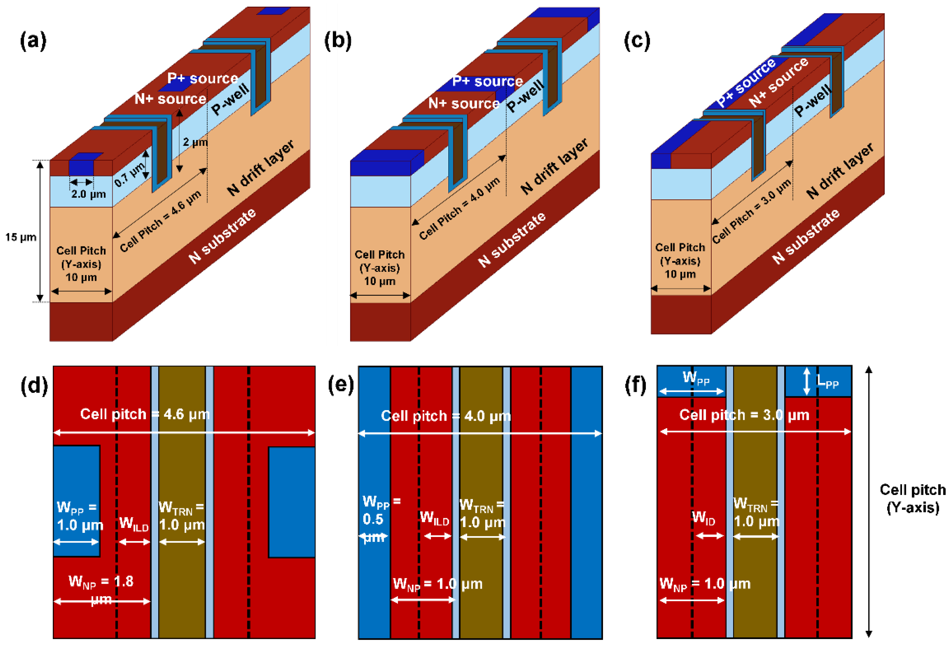
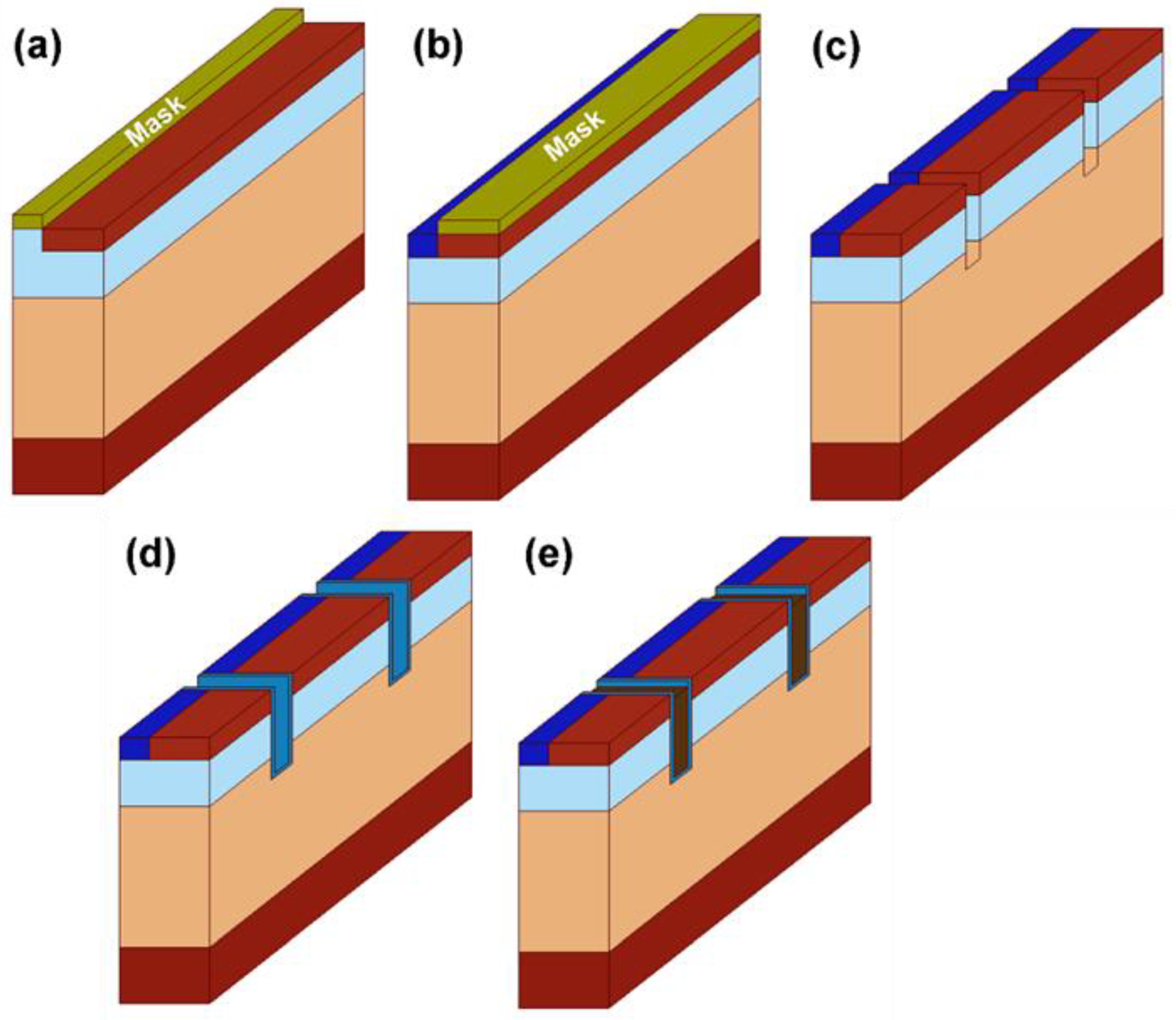

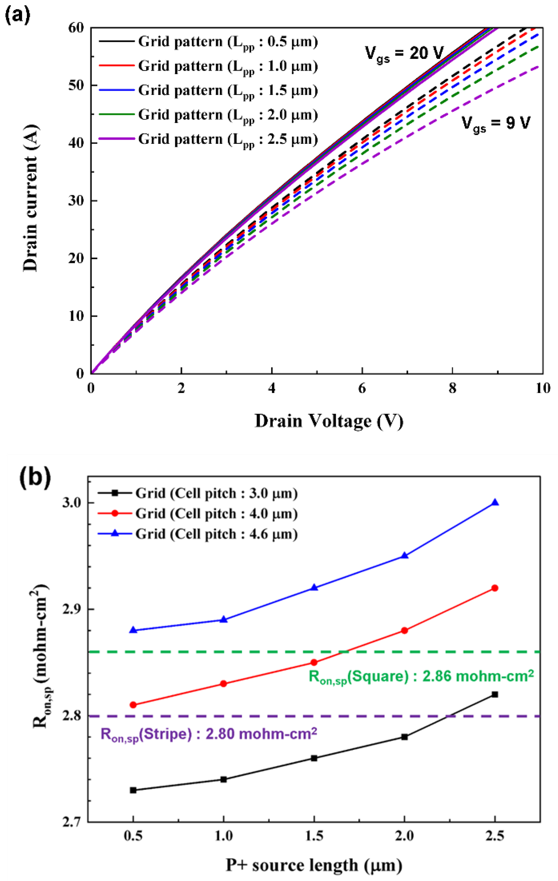
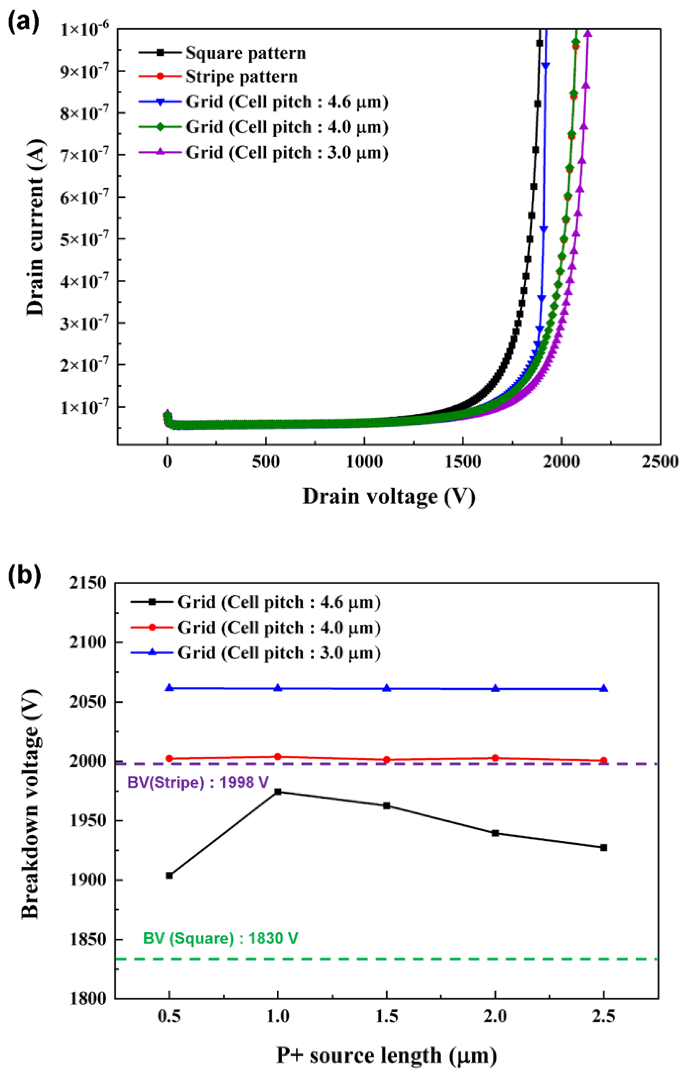
| Parameter | Value | Unit |
|---|---|---|
| Thickness of drift layer | 15 | μm |
| Doping concentration of drift layer | 6 × 10¹⁵ | cm−3 |
| Trench depth and width | 2, 1 | μm |
| Doping concentration of P base | 2 × 10¹⁷ | cm−3 |
| Channel length | 0.7 | μm |
| Gate oxide thickness | 50 | nm |
| Width of inter layer dielectric (ILD) | 0.5 | μm |
| Half-width of cell pitch (y-axis) | 5 | μm |
| Half P+ source size (square pattern) | 1 × 2 | μm |
| Half P+ source size (stripe pattern) | 0.5 × 5 | μm |
| Half-width of cell pitch (square pattern) | 2.3 | μm |
| Half-width of cell pitch (stripe pattern) | 2.0 | μm |
| Half-width of cell pitch (grid pattern) | 1.5 | μm |
| Half-width of P+ source (grid pattern) | 1.5 | μm |
| Half-length of P+ source (grid pattern) | 0.5–2.5 (+0.5) | μm |
| Device Structure | Simulation Results | ||
|---|---|---|---|
| Specific On-Resistance (Ron,sp) [mOhm-cm2] | Forward Blocking (BV) [V] | Figure-of-Merit (FOM) [MW/cm2] | |
| Square pattern (CP = 4.6 μm) | 2.86 | 1830 | 1172 |
| Stripe pattern (CP = 4.0 μm) | 2.80 | 1998 | 1426 |
| Grid pattern (CP = 3.0 μm, Lpp = 0.5 μm) | 2.73 | 2061 | 1556 |
| Grid pattern (CP = 3.0 μm, Lpp = 1.0 μm) | 2.74 | 2061 | 1549 |
| Grid pattern (CP = 3.0 μm, Lpp = 1.5 μm) | 2.76 | 2061 | 1539 |
| Grid pattern (CP = 3.0 μm, Lpp = 2.0 μm) | 2.78 | 2061 | 1526 |
| Grid pattern (CP = 3.0 μm, Lpp = 2.5 μm) | 2.82 | 2061 | 1508 |
| Grid pattern (CP = 4.0 μm, Lpp = 0.5 μm) | 2.81 | 2002 | 1426 |
| Grid pattern (CP = 4.0 μm, Lpp = 1.0 μm) | 2.83 | 2003 | 1420 |
| Grid pattern (CP = 4.0 μm, Lpp = 1.5 μm) | 2.85 | 2001 | 1406 |
| Grid pattern (CP = 4.0 μm, Lpp = 2.0 μm) | 2.88 | 2002 | 1393 |
| Grid pattern (CP = 4.0 μm, Lpp = 2.5 μm) | 2.92 | 2000 | 1370 |
| Grid pattern (CP = 4.6 μm, Lpp = 0.5 μm) | 2.88 | 1903 | 1260 |
| Grid pattern (CP = 4.6 μm, Lpp = 1.0 μm) | 2.89 | 1974 | 1347 |
| Grid pattern (CP = 4.6 μm, Lpp = 1.5 μm) | 2.92 | 1962 | 1320 |
| Grid pattern (CP = 4.6 μm, Lpp = 2.0 μm) | 2.95 | 1939 | 1274 |
| Grid pattern (CP = 4.6 μm, Lpp = 2.5 μm) | 3.00 | 1927 | 1238 |
Disclaimer/Publisher’s Note: The statements, opinions and data contained in all publications are solely those of the individual author(s) and contributor(s) and not of MDPI and/or the editor(s). MDPI and/or the editor(s) disclaim responsibility for any injury to people or property resulting from any ideas, methods, instructions or products referred to in the content. |
© 2022 by the authors. Licensee MDPI, Basel, Switzerland. This article is an open access article distributed under the terms and conditions of the Creative Commons Attribution (CC BY) license (https://creativecommons.org/licenses/by/4.0/).
Share and Cite
Jeong, J.-H.; Jang, M.-S.; Seok, O.; Lee, H.-J. Effect of P+ Source Pattern in 4H-SiC Trench-Gate MOSFETs on Low Specific On-Resistance. Appl. Sci. 2023, 13, 107. https://doi.org/10.3390/app13010107
Jeong J-H, Jang M-S, Seok O, Lee H-J. Effect of P+ Source Pattern in 4H-SiC Trench-Gate MOSFETs on Low Specific On-Resistance. Applied Sciences. 2023; 13(1):107. https://doi.org/10.3390/app13010107
Chicago/Turabian StyleJeong, Jee-Hun, Min-Seok Jang, Ogyun Seok, and Ho-Jun Lee. 2023. "Effect of P+ Source Pattern in 4H-SiC Trench-Gate MOSFETs on Low Specific On-Resistance" Applied Sciences 13, no. 1: 107. https://doi.org/10.3390/app13010107
APA StyleJeong, J.-H., Jang, M.-S., Seok, O., & Lee, H.-J. (2023). Effect of P+ Source Pattern in 4H-SiC Trench-Gate MOSFETs on Low Specific On-Resistance. Applied Sciences, 13(1), 107. https://doi.org/10.3390/app13010107


