Article

Ku-Band CMOS Power Amplifier with Three-Stack Power Stage to Enhance Output Power and Efficiency

1
School of Electronic Engineering, College of Information Technology, Soongsil University, Seoul 06978, Korea
2
Department of Electronics Engineering, Chungnam National University, Deajeon 34134, Korea
*
Author to whom correspondence should be addressed.
Appl. Sci. 2022, 12(9), 4432; https://doi.org/10.3390/app12094432
Submission received: 20 March 2022 / Revised: 24 April 2022 / Accepted: 25 April 2022 / Published: 27 April 2022
(This article belongs to the Special Issue Recent Research in Microwave and Millimeter-Wave Components)

Abstract

:
In this study, we proposed a power amplifier structure with improved efficiency while securing high output power. First, the characteristics of the common-source and stack structures were investigated. In particular, the output power and output impedance characteristics of the stack structure were analyzed compared with the common-source structure. A common-source structure was applied to the driver stage to minimize dc power consumption, and a stack structure was applied to the power stage to ensure high output power. In order to verify the proposed structure, a Ku-band power amplifier was designed using the 65-nm RF CMOS process that provides nine metal layers. At the operating frequency of 15 GHz, saturation output power and maximum power-added efficiency were confirmed to be 22.1 dBm and 17.2%, respectively.

1. Introduction

With the recent rapid development of wireless communication technology, commercialization of 5th generation mobile communication technology in millimeter-wave bands is becoming visible. Thanks to the development of such 5th generation mobile communication technology, research into beamforming transceivers is also being actively conducted [1,2,3].
In particular, a Ku-band is used as the frequency band for satellite communications with 10.7–12.75 GHz for downlink and 13.75–14.6 GHz for uplink [4,5,6]. Considering the heavy free-space loss in satellite communications, it is possible to reduce the output power requirement for a single power amplifier by spatially combining power using a large-scale phased-array transmitter such as a beamforming system [6,7]. The beamforming technology provides various technical advantages in wireless communication and radar systems. However, unlike the previous system, a large number of high-frequency circuit units are required to be used, and, accordingly, various tasks to be solved are generated. In particular, heat generated by a large number of high-frequency circuit units degrades the high-frequency characteristics of circuits, which is a major cause of deteriorating the performance of the entire system. Therefore, for practical implementation and commercialization of a beamforming system, it is essential to efficiently dissipate heat generated at the front end of the transceiver; a more fundamental way is to suppress heat generation itself. In order to efficiently suppress heat generation in the beamforming system, it is important to improve the efficiency of a power amplifier that uses the most power at the front end of the transceiver [8,9,10].
Accordingly, studies to improve the efficiency of the power amplifier are being conducted very actively to date. However, since the output power of the power amplifier and the efficiency are in a trade-off relationship, it is required to ensure high output power and minimize efficiency degradation. Most research related to improving the efficiency of the power amplifier is focused on improving efficiency in the power stage, which consumes the most dc power. However, dc power consumption in the driver stage for driving the power stage cannot be ignored. Therefore, to improve the efficiency of the entire power amplifier, it is reasonable to reduce the dc power consumption not only in the power stage but also in the driver stage. As a result, it is required to consider the entire structure of the power amplifier, including the driver stage as well as the power stage, in order to ensure high output power and minimize efficiency degradation.
In this study, we investigated the power and driver stages that comprise a power amplifier to improve output power while suppressing degradation of the efficiency. Based on this, we proposed the structure of the driver stage and power stage to improve the efficiency of the CMOS-based Ku-band power amplifier for beamforming systems of satellite communications and verified its feasibility through verification design. In Section 2, we investigated the output power, impedance, and efficiency characteristics of the common-source and stack structures. Section 3 presents the proposed power amplifier structure. The simulation results of the designed power amplifier are shown in Section 4. Finally, we provide the measurement results of the designed power amplifier in Section 5.

2. Typical CMOS Power Amplifiers

In general, the power amplifier is designed to have the same structure as the driver and power stages constituting the power amplifier for the use of a single supply voltage. For example, both the driver and power stages are designed in a common-source structure or a cascode structure [11]. This design method has the advantage of using a single supply voltage in the power amplifier and suggests that each of the driver and power stages has room for additional structural optimization. In this study, the structures most commonly used in the typical power amplifiers were investigated. Based on this, an optimum structure of a power amplifier to obtain high output power and high efficiency is proposed.

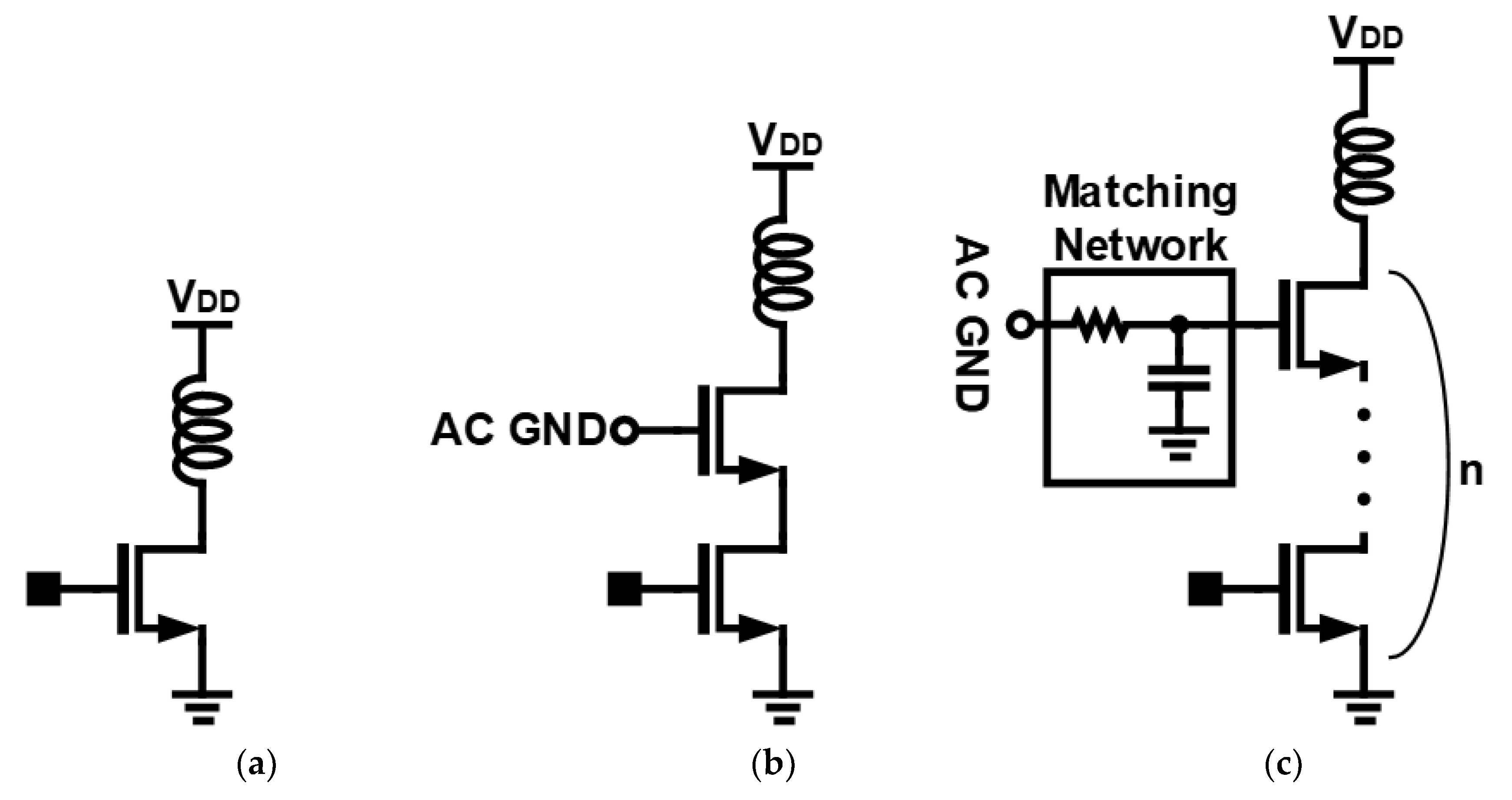
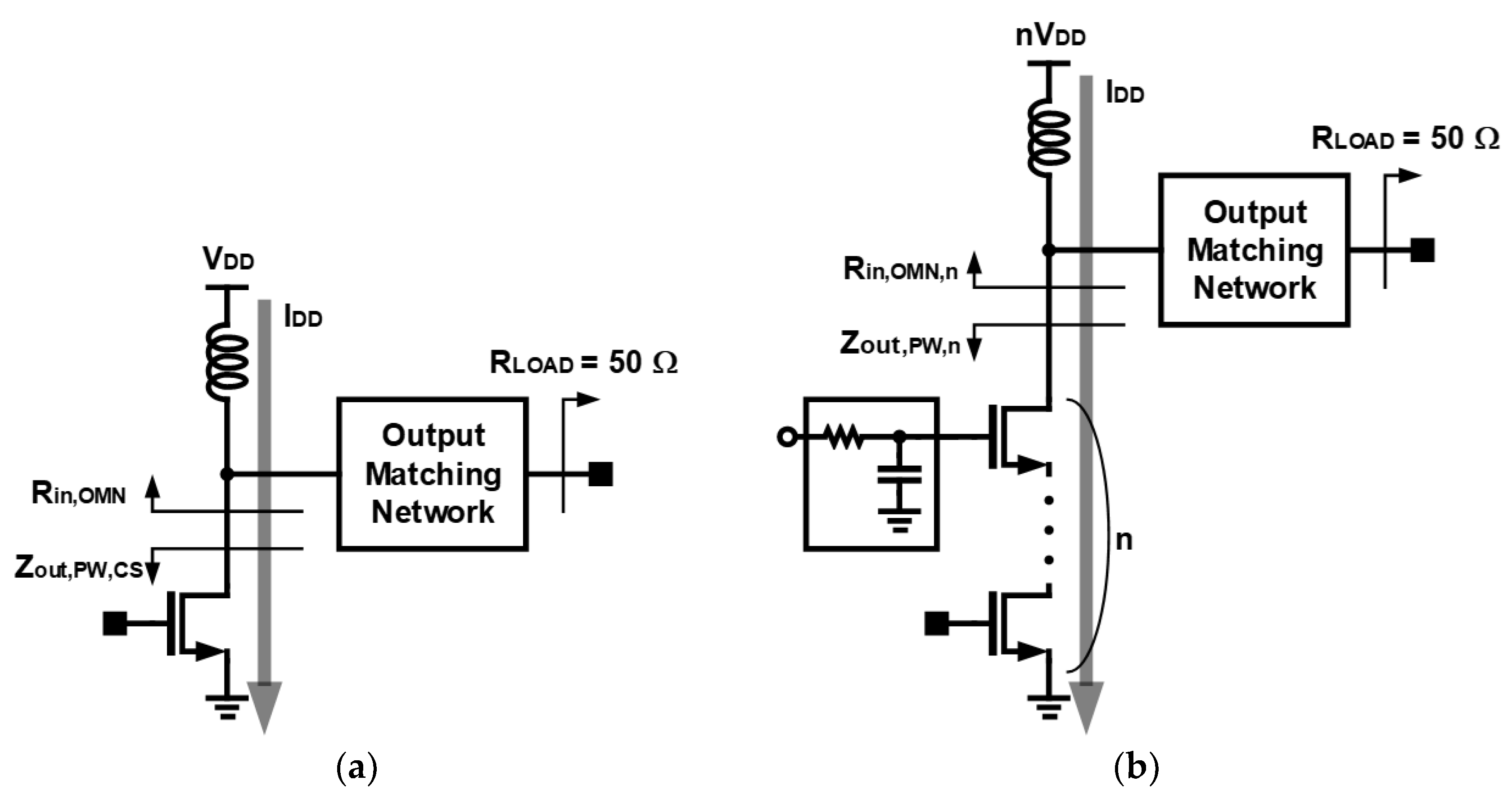
2.1. Common-Source Structure

In the case of a general power amplifier, a power stage for securing high output power and a driver stage for securing sufficient power gain are included. In the case of the driver stage, relatively less dc power is consumed compared with the power stage. However, the dc power consumption in the driver stage is a level that cannot be ignored in terms of dc power consumption of the entire power amplifier.
The circuit structure commonly used for the driver stage and power stage of the power amplifier is a common-source structure and a cascode structure, as illustrated in Figure 1. In the case of a common-source structure, a relatively low power supply voltage is used in consideration of the breakdown voltage of the transistor. Accordingly, there is an advantage that the power consumption calculated as the product of the voltage and the current is relatively small. On the other hand, since a low supply voltage is used, it is relatively difficult to sufficiently secure an output power proportional to the square of the supply voltage. In addition, in the case of low power supply voltage and 50 Ω load conditions, there is a disadvantage in that the sensitivity of the output matching characteristics to variations in the device values constituting the output matching network is high.

2.2. Stack Structure

In this study, a stack structure was used for the power stage to improve the output power of the power amplifier. First, compared with the common-source structure, the output characteristics of the stack structure were investigated. The stack structure of Figure 2 is designed to have the same voltage drop between the drain-source of each stacked transistor. The gate voltage and impedance of each transistor are used to control the voltage drop between the drain-source. In this case, gate impedance is generally implemented using a resistor and a capacitor.
Under the condition of 50 Ω load impedance, if the number of stacked transistors in the stack structure is n, the supply voltage of the stack structure can be n times higher than the supply voltage of the common-source structure. Therefore, the ratio of the output impedance of the common-source structure and the stack structure is as follows:
Z o u t , P W , n Z o u t , P W , C S = ( n V D D I D ) / ( V D D I D ) = n
Here, VDD and ID are the supply voltage and current of the amplifier, respectively. Zout,PW,n is the output impedance of a stack structure in which n transistors are stacked, and Zout,PW,CS is the output impedance of a common-source structure. Here, it is assumed that the current flowing through each structure is the same. As in Equation (1), Zout,PW,n has values n times higher than Zout,PW,CS. Accordingly, Zout,PW,n has values closer to 50 Ω than Zout,PW,CS, making it easier to configure the output matching network of the power stage. As a result, the stack structure can relatively mitigate the sensitivity of the output matching network compared with the common-source structure.
In general, the output power of the power amplifier is proportional to the square of the supply voltage and can be expressed by load impedance as follows [12]:
P o u t , C S ( V D D ) 2 R i n , O M N , P o u t , n ( n V D D ) 2 R i n , O M N , n
Here, Pout,CS and Pout,n are the output power of the common-source and stack structures, respectively. Rin,OMN and Rin,OMN,n are the load impedances of the power stages of the common-source and stack structures, respectively. If the Rin,OMN,n is the same as the Rin,OMN, the difference in output power between the two structures can be calculated in decibels as follows [12]:
Δ P o u t ( dB ) = P o u t , n ( dBm ) P o u t , C S ( dBm ) = 10 log ( n V D D ) 2 R i n , O M N 10 log ( V D D ) 2 R i n , O M N = 20 log n
However, since the output impedance is n times different between the common-source structure and the n-stack structure as in Equation (1), it is possible to design the load impedance of the n-stack structure to have Rin,OMN,n values n times higher than the load impedance of the common-source structure, Rin,OMN. In this case, the output power difference between the two structures is calculated in decibels as follows.
R i n , O M N , n = n R i n , O M N Δ P o u t , o p t ( dB ) = P o u t , n , o p t ( dBm ) P o u t , C S , o p t ( dBm ) = 10 log ( n V D D ) 2 R i n , O M N , n 10 log ( V D D ) 2 R i n , O M N = 10 log ( n V D D ) 2 n R i n , O M N 10 log ( V D D ) 2 R i n , O M N = 10 log n + 10 log ( V D D ) 2 R i n , O M N 10 log ( V D D ) 2 R i n , O M N = 10 log n
where, Pout,n,opt and Pout,CS,opt represent the output powers of the n-stack and the common-source structures with optimum load impedances, respectively. As can be seen from Equations (3) and (4), although there are some differences depending on the load impedance, the output power of the n-stack structure increases with the value n compared to the common-source structure.
In the case of power-added efficiency (PAE), it is generally related to the on-resistance and load impedance of the transistor. If the power loss in the matching network is ignored, the PAE can be expressed as follows:
P A E C S R i n , O M N R o n , O M N + R i n , O M N , P A E n R i n , O M N , n R o n , O M N , n + R i n , O M N , n
where PAECS and PAEn represent PAEs of the common-source and the n-stack structures, respectively. Ron,OMN and Ron,OMN,n represent the on-resistances of transistors in the common-source and n-stack structures, respectively. If Rin,OMN,n is the same as Rin,OMN, the relationship between PAECS and PAEn is as follows:
R o n , O M N , n n R o n , O M N , R i n , O M N , n = R i n , O M N P A E n R i n , O M N n R o n , O M N + R i n , O M N P A E C S > P A E n
Since the n-stack structure uses n transistors compared with the common-source structure, it is assumed that Ron,OMN,n is n times higher than Ron,OMN. If it is assumed that Rin,OMN,n is n times larger than Rin,OMN, the relationship between PAECS and PAEn is as follows:
R o n , O M N , n n R o n , O M N , R i n , O M N , n = n R i n , O M N P A E n n R i n , O M N n R o n , O M N + n R i n , O M N = R i n , O M N R o n , O M N + R i n , O M N P A E C S P A E n
From Equations (4) and (7), the n-stack structure can secure high output power while maintaining the same PAE as the common-source structure. In general, output power and PAE have a trade-off relationship. Therefore, if the n-stack and the common-source structures are designed to have the same output power, this means that the efficiency of the n-stack structure can be improved.

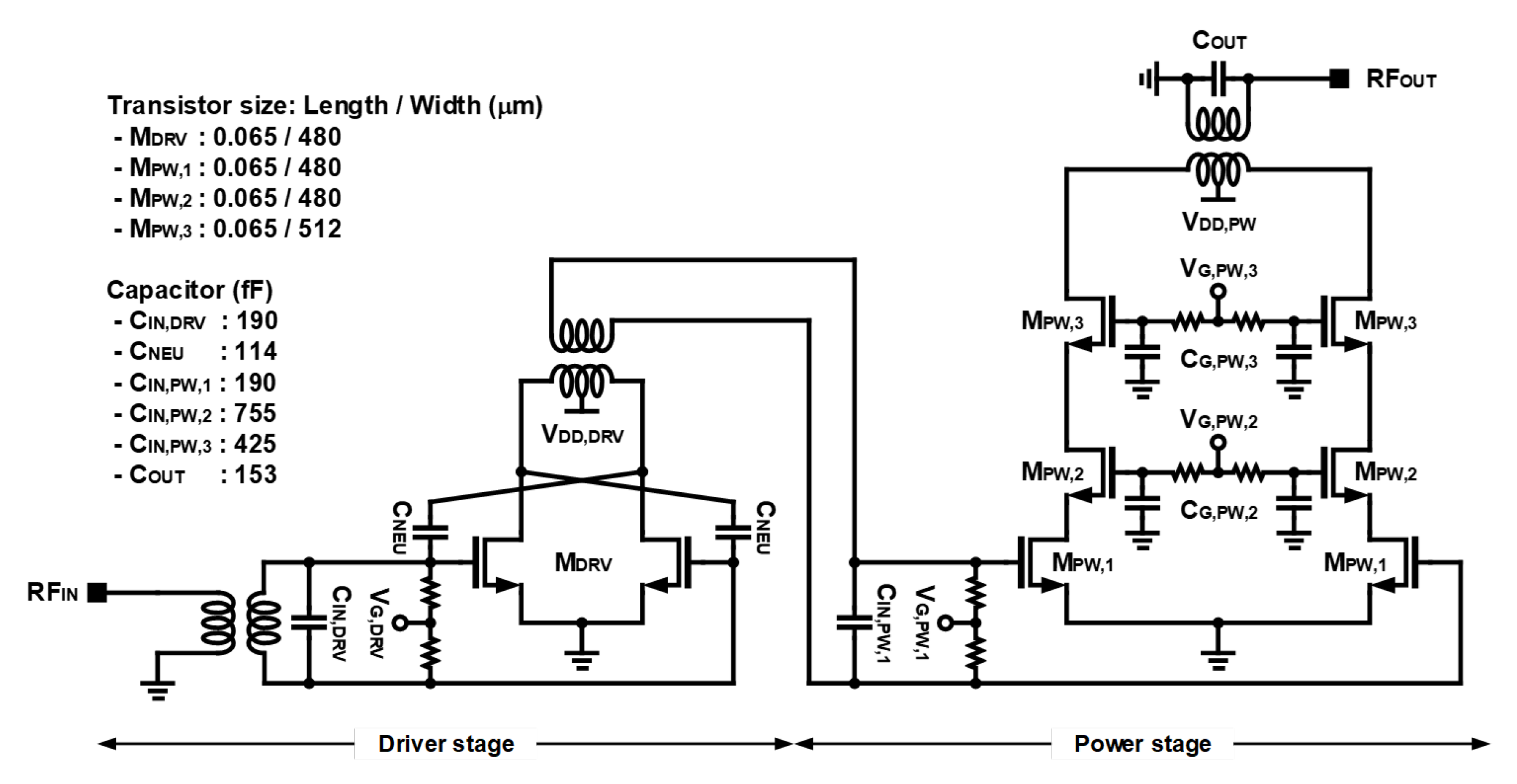
3. Proposed Power Amplifier

In this study, we took only the advantages of the common-source and stack structures and proposed a structure capable of improving the efficiency of the power amplifier. The driver stage of the power amplifier requires relatively low output power compared with the power stage. Therefore, in this study, the driver stage was implemented in a common-source structure with low power consumption. Through this, it was intended to increase efficiency by reducing the power consumption of the entire power amplifier. In the case of the power stage, ensuring high output power plays a major role, so it was easy to ensure output power by forming a power stage in the stack structure and using high supply voltage.
As a result, the stack structure was applied only to the power stage, which ensures high power, and the common-source structure was applied to the driver stage to minimize power consumption. Through this, we designed a power amplifier that can improve efficiency while securing high output power.

4. Design of the Proposed Power Amplifier

In this work, we designed the power amplifier operating in the Ku-band using a 65-nm RF CMOS process that provides nine metal layers to verify the feasibility of the proposed power amplifier structure. Figure 3 shows the designed power amplifier’s schematic. The input and output matching networks were completed using transformers and capacitors serving as Balun. All resistors used the same value of 5.5 kΩ.
The designed power amplifier’s driver stage has a common-source structure, and a neutralization capacitor was applied between a gate and a drain of the differential structure to ensure the stability of the power amplifier. Since the driver stage has a common-source structure, the power supply voltage was set to 1.0 V in consideration of the breakdown voltage of the transistor.
In this study, the power stage was designed in a stack structure to ensure high output power. The number of transistors forming the stack structure depends on the operating frequency and the target output power. In order to obtain an output power of at least 20 dBm in the Ku-band, a stack structure was formed of three transistors, and a matching network, including a resistor and a capacitor, was connected to the gate of the stacked transistor so that voltage drops in each transistor were the same. Because the power stage has a stacked structure and voltages are divided and applied to three transistors, a high-power voltage of 2.6 V was used to facilitate and ensure a high output power.
Figure 4 shows the load–pull results in the power stage. As a result of the load–pull simulation, at an operating frequency of 15 GHz, the maximum output power is 24.5 dBm, and the maximum PAE is 40.4%. For power matching, the output matching network was composed of a transformer and an additional MIM capacitor. As shown in Figure 4, the input impedance of the output matching network at an operating frequency of 15 GHz is designed to be located between the maximum output power and the maximum PAE points. In the load–pull simulation, the output power and PAE contour lines have an interval of 0.5 dB and 2%, respectively. Therefore, assuming that there is no power loss in the matching network under the selected load impedance condition, as can be observed in Figure 4, the output power and PAE are higher than 24.0 dBm and 38.4%, respectively.
Figure 5 shows the simulation results of the S-parameters. The power amplifier was designed to have the highest gain at an operating frequency of 15 GHz. The output matching network of the power amplifier was designed with the power matching technique. Figure 6 shows the simulation results of the power gain and PAE depending on the output power in slow, typical, and fast corners. A corner simulation was performed to design the power amplifier optimized for a typical corner. Figure 7 shows the simulation results of the power gain and PAE depending on the output power at operating temperatures −20 °C, 25 °C, and 80 °C. As can be observed in Figure 7, Psat and PAE show similar results depending on the temperature.
Figure 8 shows the simulated current at the driver and power stages at an operating frequency of 15 GHz. Figure 9 shows simulated saturation power (Psat), gain, P1dB, and PAE according to the frequency at an operating temperature of 25 °C. As can be observed in Figure 9, the power amplifier was optimized at an operating frequency of 15 GHz.

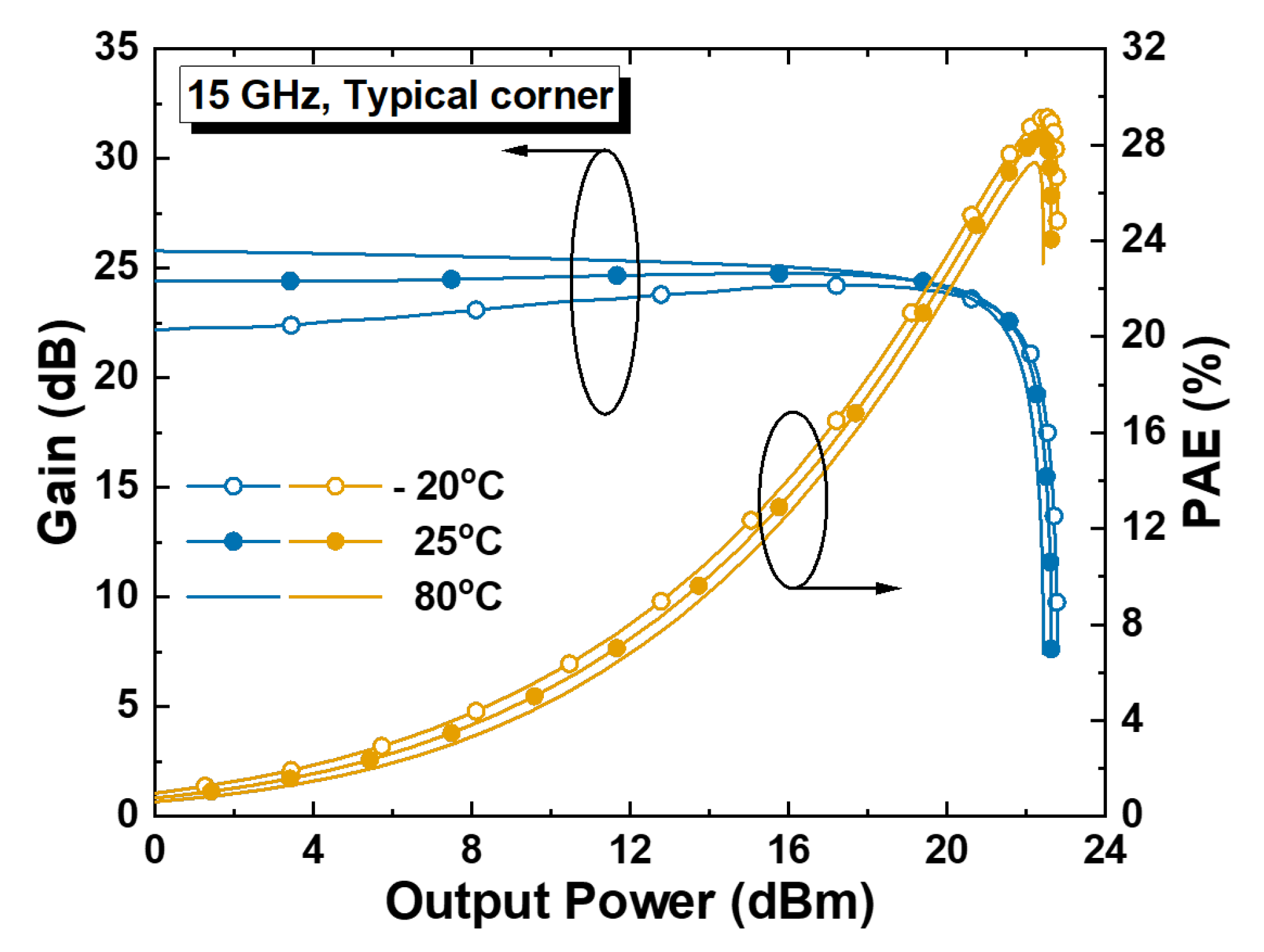
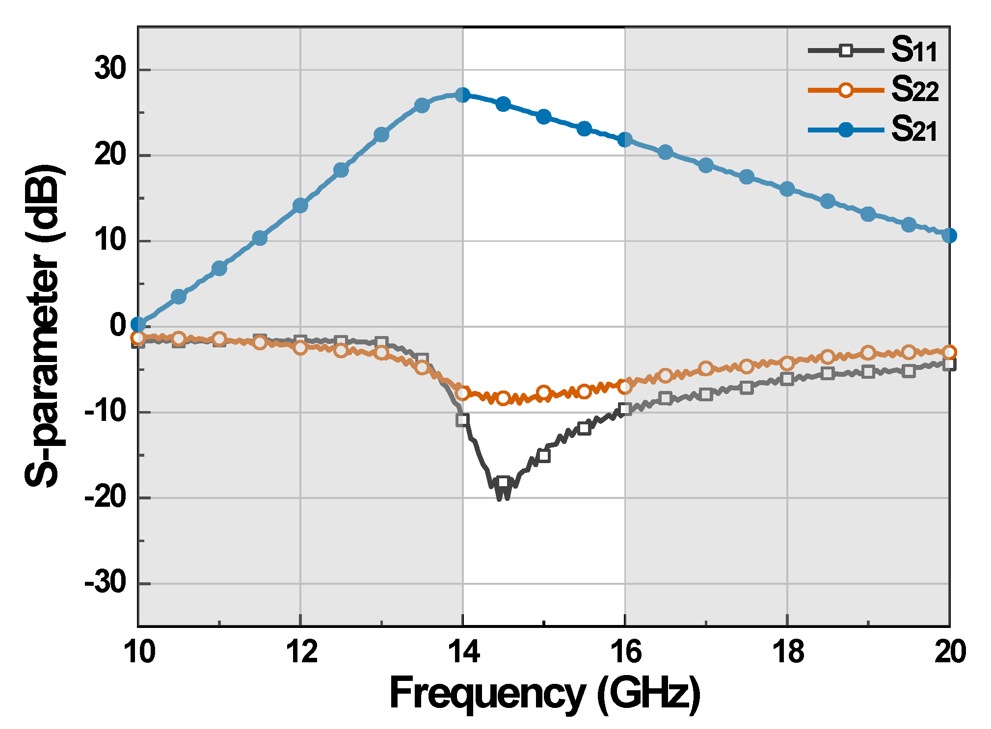
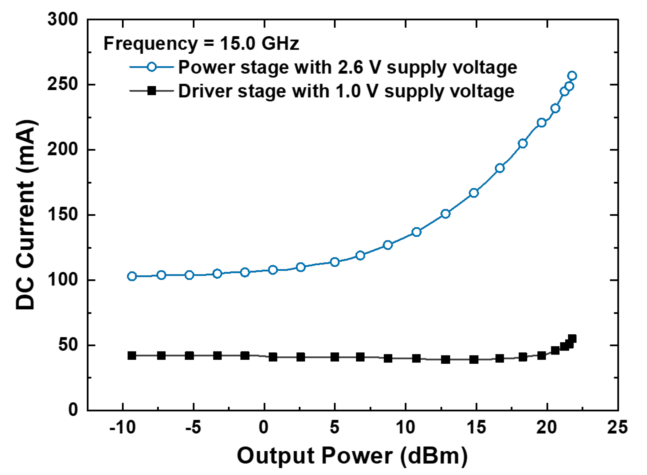
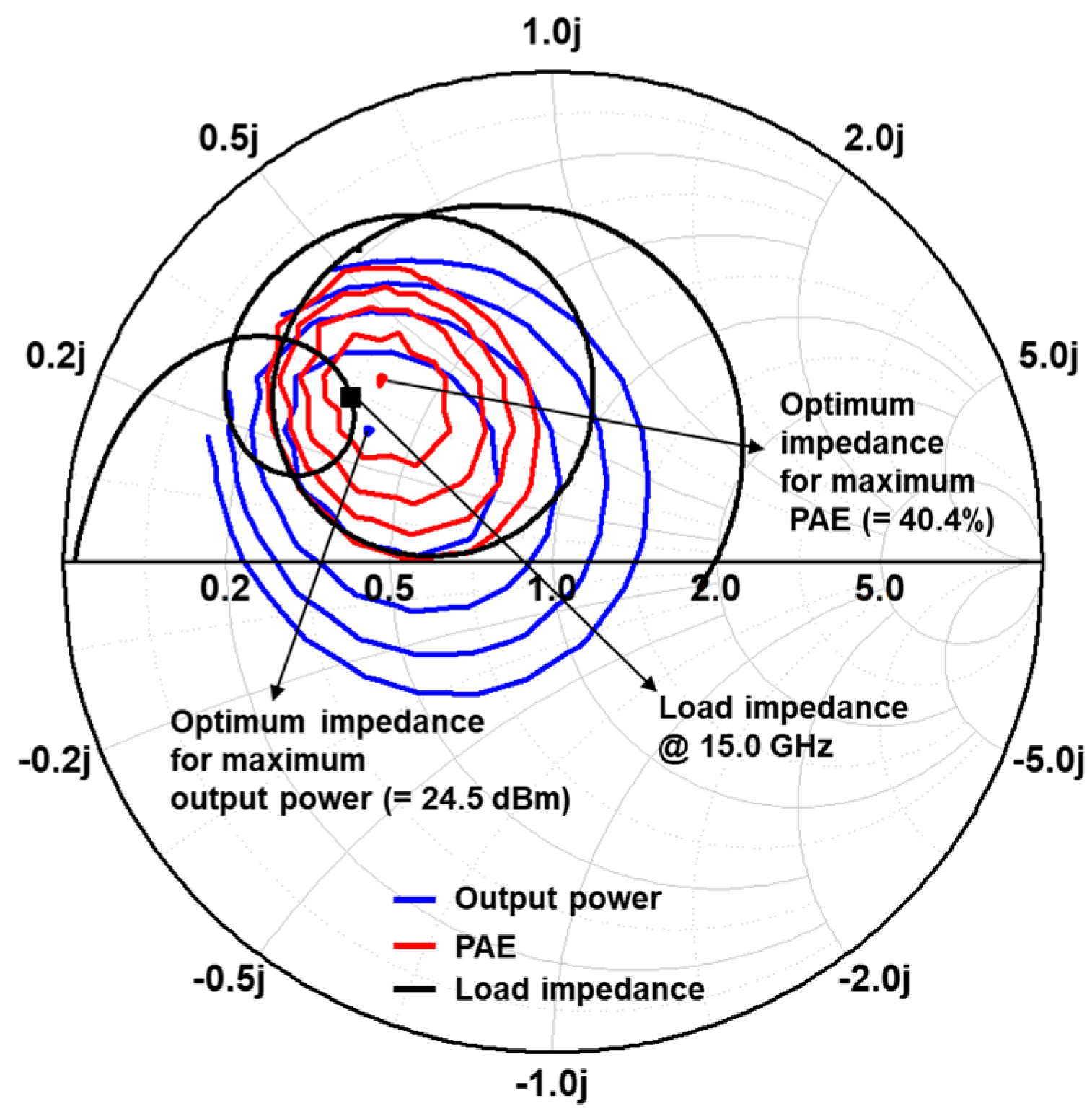
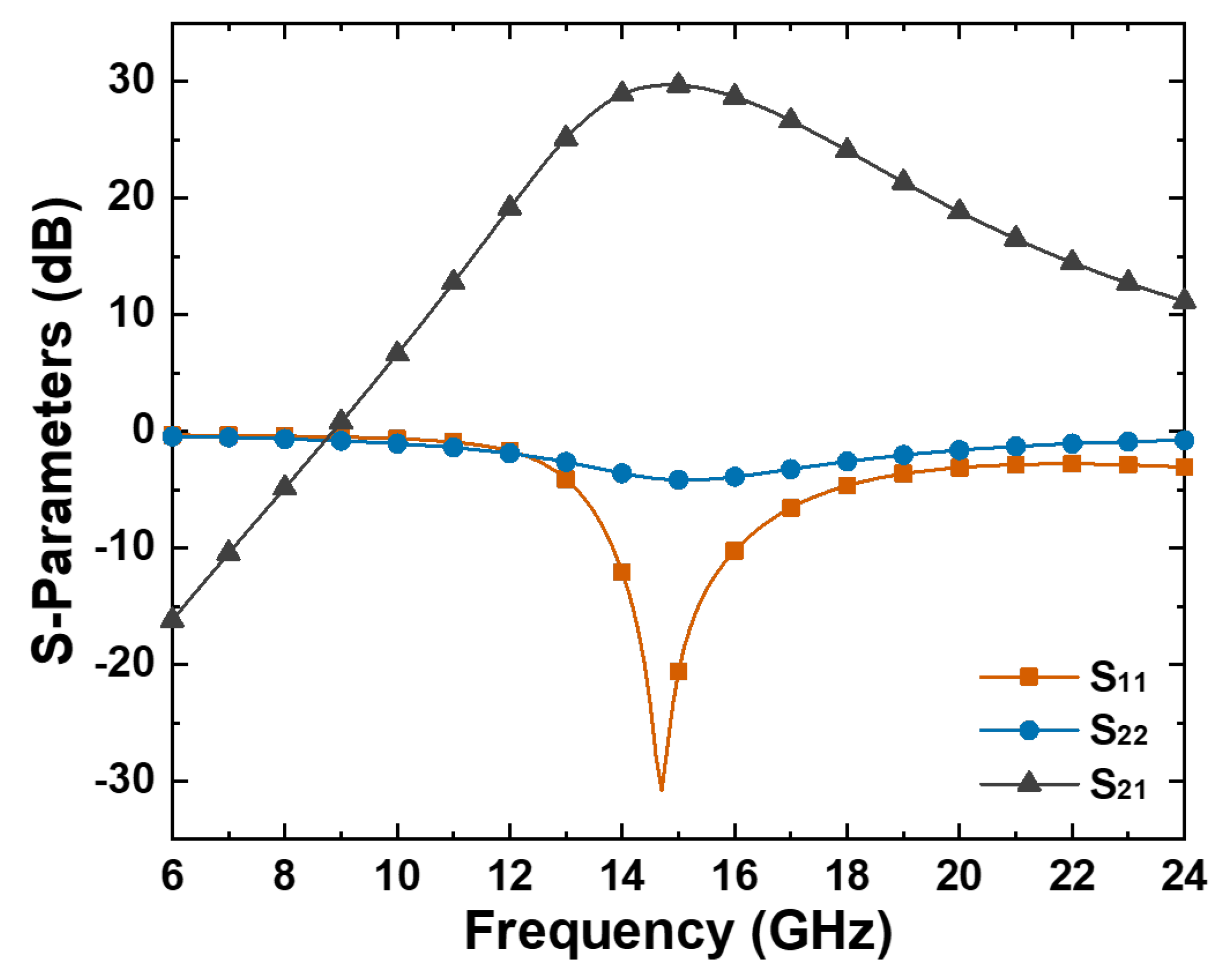
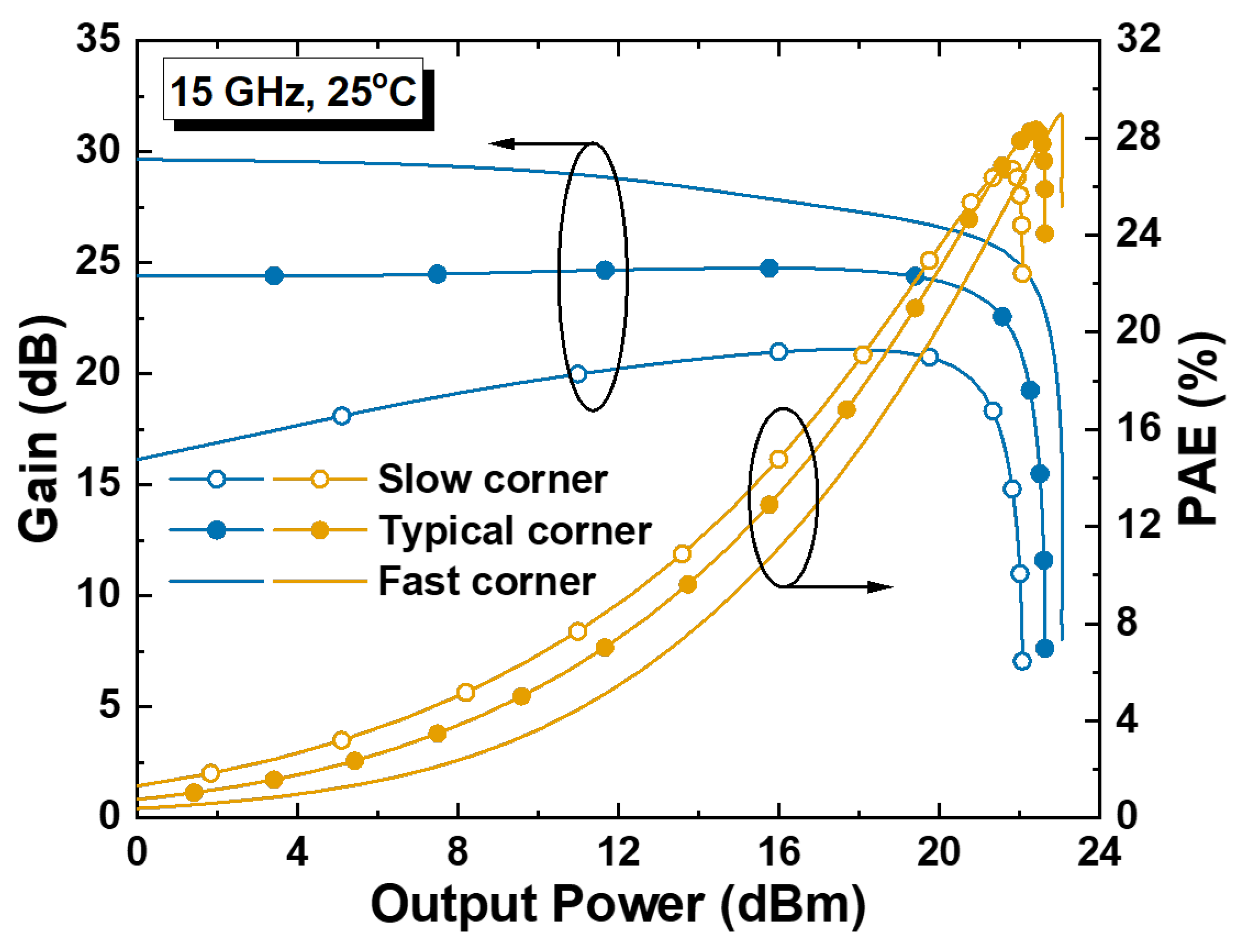
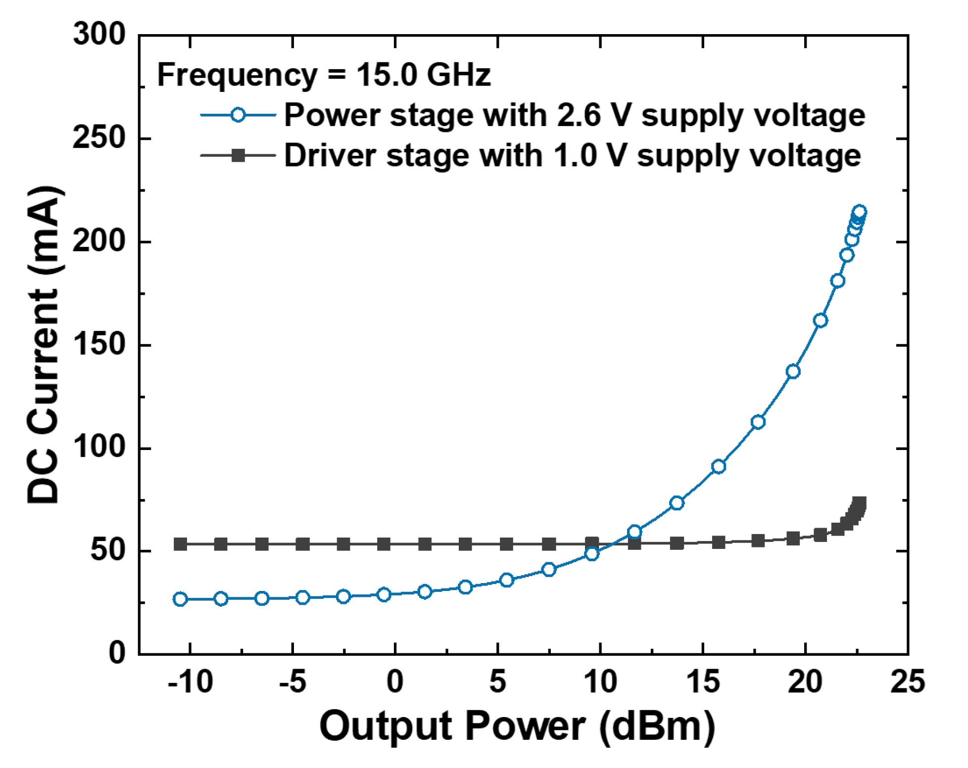
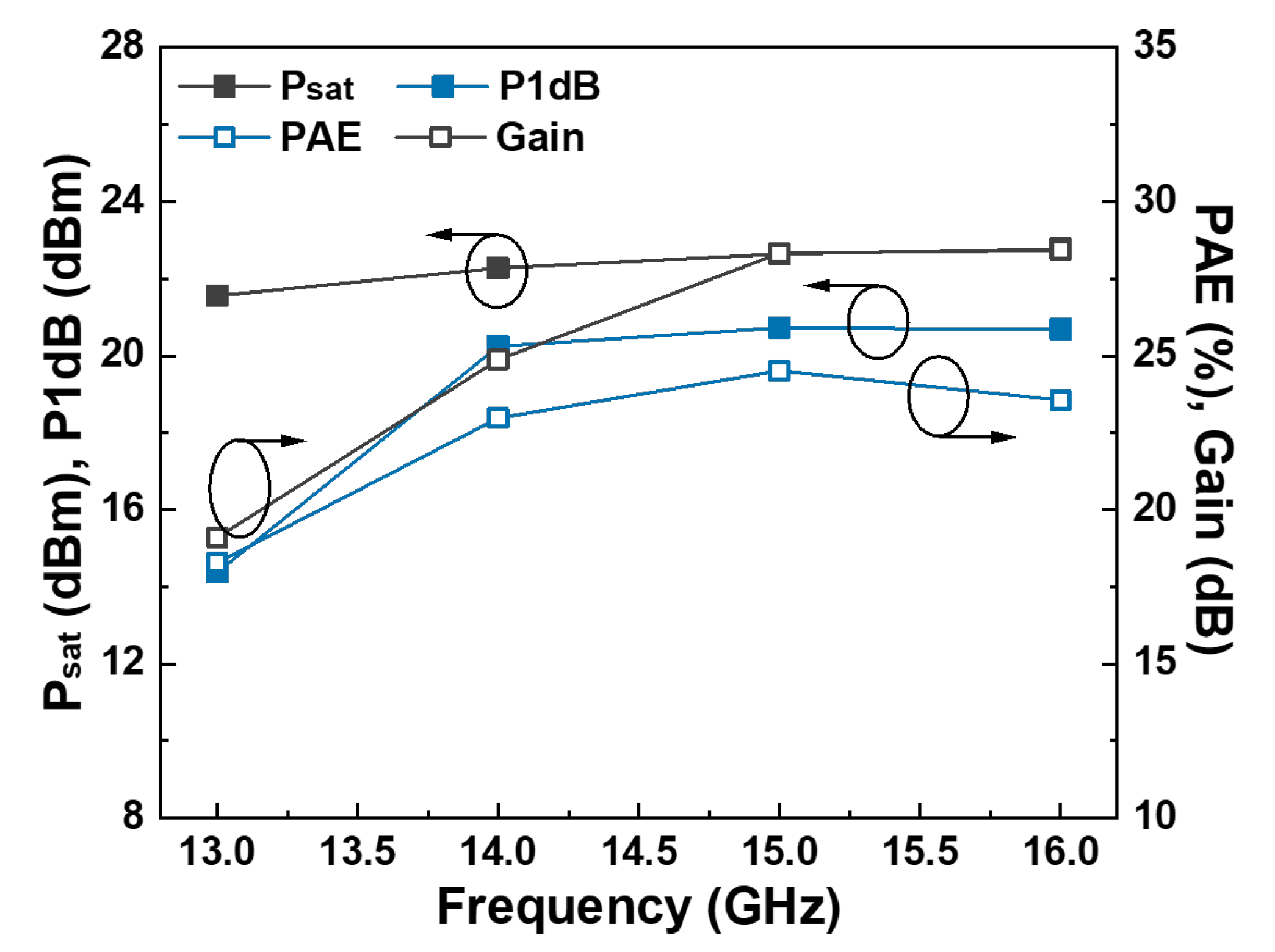
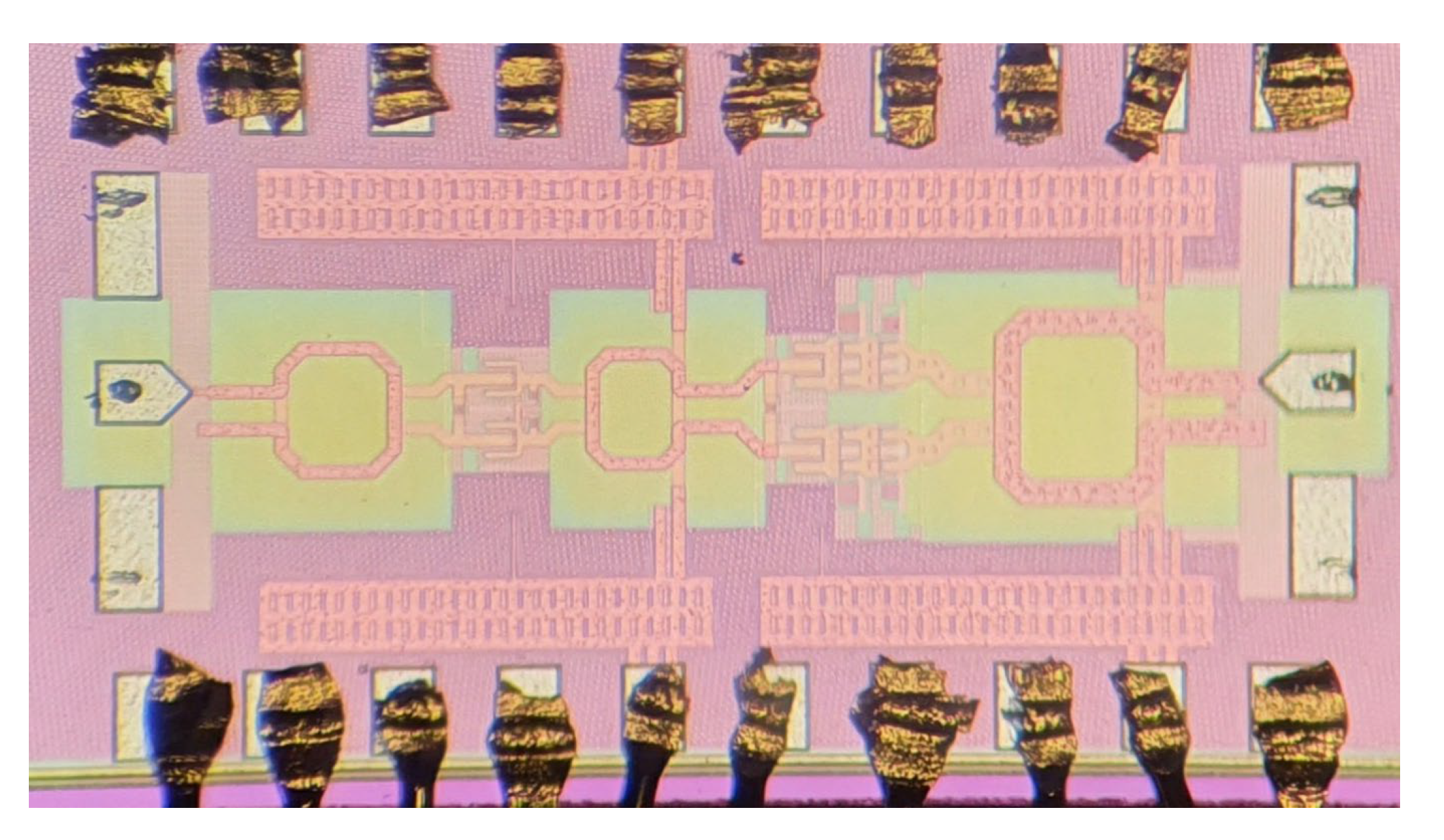
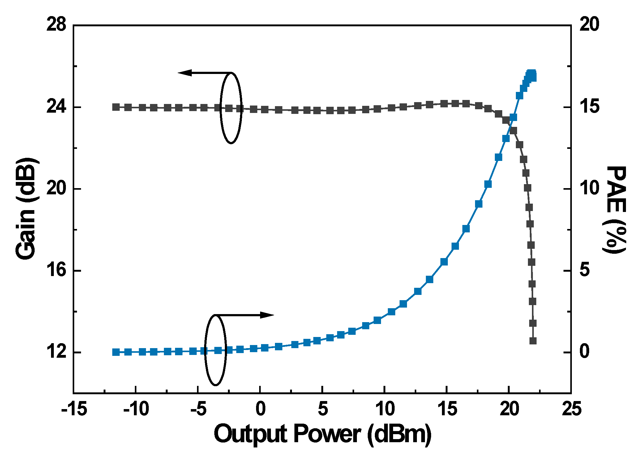
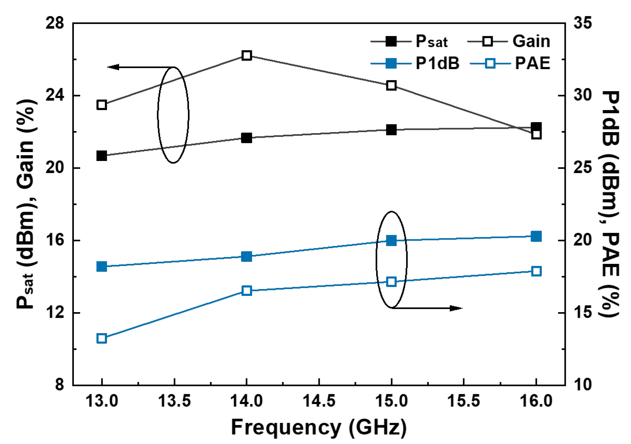
5. Measurement Results

A transformer was used for the matching network between the driver and power stages, and a supply voltage of the driver stage was applied through a center tab of the transformer. The designed driver stage used a gate voltage of 0.4 V for the Class-AB operation, and the gate voltages of VG,PW,1, VG,PW,2, and VG,PW,3 were 0.3 V, 1.7 V, and 2.6 V, respectively. The supply voltages of the driver and power stages were 1.0 V and 2.6 V, respectively. Measurements were carried out at room temperature.
Figure 10 is a chip photograph of the designed power amplifier. The total size, including the test pad, is 0.725 × 0.500 mm2. DC bias was applied through boning wires, and a GSG probe was used for the RF signals. Figure 11 shows the measured S-parameters of the designed power amplifier. Because the power stage was designed with the power matching technique, the measured value of S22 was higher than that of S11. Due to parasitic effects that were not predicted by electromagnetic (EM) simulation, compared with the simulation results, the measured optimum frequency was downshifted.
Figure 12 shows the power gain and power-added efficiency (PAE) according to the output power at the center frequency of 15 GHz. The measured Psat is 22.1 dBm, and the maximum PAE is 17.2%. Figure 13 shows the measured current at the driver and power stages. As the supply voltage for the driver stage was 1.0 V, the dc power consumption in the driver stage was minimized. In the process of optimizing the dc bias to obtain a high P1dB during measurement, the amount of dc current in the power stage increased compared with the simulation. Figure 14 shows measured Psat, gain, P1dB, and PAE according to frequency. The measured output power and PAE were degraded when compared with the simulation results shown in Figure 9. It is predicted that this is due to the lack of accuracy of the EM simulation and the dummy patterns to satisfy the design rule. In particular, as the bias values in the measurement were optimized to ensure P1dB, the degradation of the measured PAE increased compared with the simulation. At the 15 GHz operating frequency, the measured P1dB compared with the simulation degraded by approximately 0.7 dB, but in the case of PAE, it degraded by approximately 7.3%.
Table 1 shows a comparison of the performance of the designed power amplifier with that of state-of-the-art CMOS power amplifiers. As shown in Table 1, the PAE itself of the proposed power amplifier seems to be somewhat low. However, it should be considered that P1dB, Psat, and PAE are trade-offs with each other. In particular, in the case of a power amplifier composed of only a power stage, the efficiency decreases when considering the design of an essential driver stage. An additional output power improvement can be expected if an additional power combining technique, such as reference [13], is applied to the power stage.

6. Conclusions

In this paper, we proposed a structure of a power amplifier to ensure high output power and to improve efficiency by designing a driver stage in a common-source structure and a power stage in a stack structure. In order to derive the proposed structure, the output power and output impedance characteristics of the stack structure were compared with the common-source structure and analyzed. To verify the feasibility of the proposed structure, the Ku-band power amplifier was designed using the 65-nm RF CMOS process. At an operating frequency of 15 GHz, saturation output power and maximum power-added efficiency were confirmed to be 22.1 dBm and 17.2%, respectively.

Author Contributions

Conceptualization, J.Y., H.J. and C.P.; methodology, J.L. and S.J.; investigation, J.L., H.J. and C.K.; supervision, writing—original draft, C.P.; writing—review and editing, J.Y. and C.P. All authors have read and agreed to the published version of the manuscript.

Funding

This research was funded in part by the National Research Foundation of Korea (NRF) grant funded by the Korean government (MSIT) (No. 2021R1A2C1013666) and in part by the National Research Foundation of Korea (NRF) grant funded by the Korean government (MSIT) (No. NRF-2021R1A4A1032580).

Institutional Review Board Statement

Not applicable.

Informed Consent Statement

Not applicable.

Data Availability Statement

The data can be obtained from the authors on request.

Conflicts of Interest

The authors declare no conflict of interest.

References

  1. Cho, G.; Jeong, G.; Hong, S. 28-GHz CMOS power amplifier linearized with resistive drain-body connection. IEEE Microw. Wirel. Compon. Lett. 2020, 30, 876–879. [Google Scholar] [CrossRef]
  2. Ding, B.; Yuan, S.; Zhao, C.; Tao, L.; Tian, T. A Ka band FMCW transceiver front-end with 2-GHz bandwidth in 65-nm CMOS. IEEE Trans. Circuits Syst. II-Express Briefs 2019, 66, 212–216. [Google Scholar] [CrossRef]
  3. Jia, H.; Prawoto, C.C.; Chi, B.; Wang, Z.; Yue, C.P. A full Ka-band power amplifier with 32.9% PAE and 15.3-dBm power in 65-nm CMOS. IEEE Trans. Circuits Syst. I-Regul. Pap. 2018, 65, 2657–2668. [Google Scholar] [CrossRef]
  4. Jong, G.D.; Leenaerts, D.; van der Heijden, E. A fully integrated down-converter for Ka-band VSAT satellite reception. In Proceedings of the ESSCIRC (ESSCIRC), Bordeaux, France, 17–21 September 2012. [Google Scholar]
  5. Maassen, D.; Rautschke, F.; Ohnimus, F.; Schenk, L.; Dalisda, U.; Boeck, G. 70 W GaN-HEMT Ku-band power amplifier in MIC technology. IEEE Trans. Microw. Theory Technol. 2017, 65, 1272–1283. [Google Scholar] [CrossRef]
  6. Zhong, J.; Zhao, D.; You, X. A Ku-Band CMOS Power Amplifier with Series-Shunt LC Notch Filter for Satellite Communications. IEEE Trans. Circuits Syst. I-Regul. Pap. 2021, 68, 1869–1880. [Google Scholar] [CrossRef]
  7. Aljuhani, A.H.; Kanar, T.; Zihir, S.; Rebeiz, G.M. A scalable dual-polarized 256-element Ku-band SATCOM phased-array transmitter with 36.5 dBW EIRP per polarization. In Proceedings of the European Microwave Conference (EuMC), Madrid, Spain, 23–27 September 2018. [Google Scholar]
  8. Nasri, A.; Estebsari, M.; Toofan, S.; Piacibello, A.; Pirola, M.; Camarchia, V.; Ramella, C. Design of a Wideband Doherty Power Amplifier with High Efficiency for 5G Application. Electronics 2021, 10, 873. [Google Scholar] [CrossRef]
  9. Xu, Y.; Pang, J.; Wang, X.; Zhu, A. Enhancing Bandwidth and Back-Off Range of Doherty Power Amplifier With Modified Load Modulation Network. IEEE Trans. Microw. Theory Tech. 2021, 69, 2291–2303. [Google Scholar] [CrossRef]
  10. Lv, G.; Chen, W.; Chen, X.; Ghannouchi, F.M.; Feng, Z. A Fully Integrated 47.6% Fractional Bandwidth GaN MMIC Distributed Efficient Power Amplifier with Modified Input Matching and Power Splitting Network. IEEE Trans. Microw. Theory Tech. 2021, 69, 3132–3145. [Google Scholar] [CrossRef]
  11. Jeong, H.; Lee, H.; Park, B.; Jang, S.; Kong, S.; Park, C. Optimization Technique for High-Gain CMOS Power Amplifier for 5G Applications. Appl. Sci. 2021, 11, 11691. [Google Scholar] [CrossRef]
  12. Park, C.; Kim, Y.; Kim, H.; Hong, S. A 1.9-GHz CMOS Power Amplifier Using Three-Port Asymmetric Transmission Line Transformer for a Polar Transmitter. IEEE Trans. Microw. Theory Tech. 2007, 55, 230–238. [Google Scholar] [CrossRef]
  13. Li, X.; Lv, W.; Li, Y.; Wang, Y.; Huang, S.; Duan, Z. A Ku-Band High-Integrated CMOS Power Amplifier. In Proceedings of the IEEE 5th International Conference on Integrated Circuits and Microsystems (ICICM), Nanjing, China, 23–25 October 2020. [Google Scholar]
  14. Chen, B.; Lou, L.; Tang, K.; Wang, Y.; Gao, J.; Zheng, Y. A 13.5–19 GHz 20.6-dB Gain CMOS Power Amplifier for FMCW Radar Application. IEEE Microw. Wirel. Compon. Lett. 2017, 27, 377–379. [Google Scholar] [CrossRef]
  15. Chen, J.; Helmi, S.R.; Jou, A.Y.; Mohammadi, S. A Wideband Power Amplifier in 45 nm CMOS SOI Technology for X Band Applications. IEEE Microw. Wirel. Compon. Lett. 2013, 23, 587–589. [Google Scholar] [CrossRef]
Figure 1. Typical structure of power amplifiers: (a) common-source, (b) cascode, and (c) stack structures.
Applsci 12 04432 g001
Figure 2. Impedances of power stages: (a) common-source and (b) stack structures.
Applsci 12 04432 g002
Figure 3. Schematic of designed power amplifier.
Applsci 12 04432 g003
Figure 4. Load–pull simulation results.
Applsci 12 04432 g004
Figure 5. Simulation results: S-parameters.
Applsci 12 04432 g005
Figure 6. Simulation results: gain and PAE according to output power in slow, typical, and fast corners.
Applsci 12 04432 g006
Figure 7. Simulation results: gain and PAE according to output power at operating temperatures −20 °C, 25 °C, and 80 °C.
Applsci 12 04432 g007
Figure 8. Simulation results: current consumptions of driver and power stages.
Applsci 12 04432 g008
Figure 9. Simulation results: Psat, P1dB, PAE, and gain depending on frequency.
Applsci 12 04432 g009
Figure 10. Photograph of the designed CMOS power amplifier (0.725 × 0.55 mm2).
Applsci 12 04432 g010
Figure 11. Measurement results: S-parameters.
Applsci 12 04432 g011
Figure 12. Measurement results: gain and PAE according to output power.
Applsci 12 04432 g012
Figure 13. Measurement results: current consumptions of driver and power stages.
Applsci 12 04432 g013
Figure 14. Measurement results: Psat, P1dB, PAE, and gain depending on frequency.
Applsci 12 04432 g014
Table 1. Performance comparison with state-of-the-art CMOS power amplifiers.
Ref.Tech.
(CMOS)
Freq.
(GHz)
Supply
(V)
Psat
(dBm)
P1dB
(dBm)
Gain
(dB)
Peak PAE
(%)
Architecture
This work65 nm15.01.0/2.622.120.024.617.22-stage/
CS + Stack
(2021)
T-CAS-1 [6]
65 nm14.21.014.5-21.924.12-stage/
CS
(2020)
ICICM [13]
65 nm14–18-22.617.426.8302-stage/
CS
(2017)
MWCL [14]
65 nm15.01.213.911.620.6203-stage/
CS
(2013)
MWCL [15]
45 nm
(SOI)
9–15 @124.822.821.99.821.81-stage/
Stack
Publisher’s Note: MDPI stays neutral with regard to jurisdictional claims in published maps and institutional affiliations.

