Abstract
During the thermal sintering of metal nanoparticles (NPs) the process temperature plays the most important role in the outcome of the sintering results and the selection of a suitable substrate. Here, temperature calculation during pulsed laser sintering of silver (Ag) nanoparticles (NPs) inkjet-printed on glass substrates is presented. During the pulsed laser sintering of Ag NPs, a minimum line resistivity less than twice the bulk silver resistivity was obtained within around 52 s under a laser power of 276 mW. The temperature field during the pulsed laser sintering of Ag NPs was estimated via a three-dimensional numerical model in which a temperature-dependent thermal conductivity of Ag NPs was adopted. An algorithm for treating the thermal conductivity of the heated Ag NPs in a region by a previous laser shot was devised for the improvement of the temperature field estimation. A maximum temperature of approximately 204 °C over the Ag NPs line was obtained with a 276 mW laser power and a scanning speed of 135 μm/s.
1. Introduction
With the increasing need for developing innovative electronics devices, new methods for patterning integrated circuits are devised to replace or compliment the conventional microcircuit patterning techniques. Conventional photolithography has been in practice since the fabrication of the first transistor in 1948 [1]. This patterning technique is costly, wasteful, and complex for large-scale fabrication [2]. Moreover, the following subtractive processes such as reactive ion etching and wet etching produce hazardous chemicals (i.e., film materials and chemical etchants) [3,4]. Since the current advances in flexible electronics demand the use of polymer and paper substrates that are sensitive to high temperatures and chemical etchants, the conventional subtractive microfabrication processes are not applicable [5]. As a potential alternative, the demonstration of a roll-to-roll printing and sintering system on polymer substrates establishes a gateway to the future of the electronic industry [6,7].
Printed electronics has facilitated the printing techniques of metal nanoparticles (NPs) for the fabrication of electronic devices such as near-field communication (NFC) tags [8], thin-film transistors [9], organic field-effect transistors (OFETs) [10], biosensors [11], and stretchable sensors [12]. Different metal NPs such as silver (Ag) [13], copper (Cu) [14], and gold (Au) [15] of different sizes ranging from 2 to 50 nm are used due to their high electrical conductivity. These metal NPs are included in inks with organic additives (binders, dispersants, and organic solvents) to prevent their agglomeration among NPs. NPs inks are printed onto various substrates to form the desired circuit patterns, followed by a sintering step to render the printed tracks conductive.
The thermal sintering is conventionally performed in an oven, which is called oven sintering. However, the oven sintering method requires high-temperature heat treatment at a minimum of around 200 °C and a long heating time of up to about 1 h or more, which limits the use of heat-vulnerable substrates such as glass, polymer, and paper. [16]. To minimize the damage, rapid sintering methods such as electrical [17], microwave [18], infrared [6], intense pulsed light [19], and laser [20] sintering methods have been extensively investigated. Among them the laser sintering method is further divided into continuous wave (CW) laser and pulsed laser sintering methods based on the mode of the laser operation. Both have their shortcomings and advantages. CW laser sintering is known to produce lower resistivities [21]; however, it induces large thermal diffusion length and is not compatible with the sintering of sub-micrometer sized patterns due to large heat affected zones [10]. On the other hand, one of the major advantages of pulsed laser sintering method is the reduced thermal diffusion length and smaller heat-affected zone at shorter pulse durations [10,22], which is crucial for the minimization of thermal damage of the substrate.
In order to use a pulsed laser for NPs sintering, it is essential to select optimum laser parameters for obtaining low electrical resistivities as well as avoiding thermal damage to the substrate in use. Laser parameters such as intensity, pulse duration and repetition rates decide the maximum sintering process temperature. Therefore, among others, accurate thermal analysis during the pulsed laser sintering is indispensable since the maximum sintering temperature is known to be highly responsible for the electrical properties and surface morphology of the Ag NPs [23]. As such, several thermal analysis studies during pulsed laser sintering of metal NPs have been reported [20,24]. A millisecond pulse laser was used by Peng et al. for the investigation of heating effects during pulsed laser sintering of Ag NPs. They estimated the Ag NPs melting temperature via theoretical calculations based on a heat diffusion model. Constant thermal conductivity of bulk Ag (429 W/m·K) was adopted in the study for the Ag NPs [25]. The calculations in the study suggested that the melting temperature of about 50 nm Ag NPs was 440 °C. Zacharatos et al. studied the thermal effects of a nanosecond pulsed laser sintering using a constant thermal conductivity of 140 W/(m·K) for the Ag NPs ink. They studied a case with a maximum of 10 laser pulses and discussed the accumulative thermal effects on the underlying polyethylene naphthalate (PEN) substrate [24]. More recently, lateral and longitudinal thermal diffusion within the copper NPs layer were elaborated during nanosecond pulsed laser sintering at different laser scanning speeds [26]. These studies considered constant thermal conductivities instead of using temperature-dependent thermal conductivity relations [26]. Bolduc et al. examined the pulse shaping effect on the heat transfer process during microsecond pulsed laser sintering of Ag NPs (50 nm) [20]. In their numerical model, to address the change in the material properties during the pulse excitation and relaxation periods of pulsed laser operation they considered a solid–liquid phase transition for the metal NPs at an estimated phase change temperature of 255 °C to simulate the real-time sintering effects. However, the melting behavior of Ag NPs (5–50 nm) has been known to be close to bulk Ag melting temperatures in multiple studies [10,27,28,29,30]. Nanoparticles tend to coalesce in an attempt to reduce their surface energy and the coalescence happen at low temperatures via solid state diffusion process. Due to the thermodynamic size effect, metal nanoparticles exhibit large melting point depression [29], e.g., 2 nm-sized nanoparticles are reported to melt at around 130–140 °C [31]. Therefore, all these limitations need to be addressed with a novel numerical model to accurately estimate the scanning pulsed laser sintering process while considering the pulsed excitation and relaxation periods with temperature-dependent thermal conductivity of Ag NPs.
In this work, we developed a numerical model that can precisely monitor the temperature field by regulating the temperature-dependent material properties (thermal conductivity and reflectivity) during the pulsed laser sintering. During a scanning pulsed laser operation each pulse induces maximum temperature within the pulse-excited location and subsequently this heating sinters the NPs. Hence maximum thermal conductivity is induced at each location where the laser pulse is incident as the NPs get sintered. Based on our developed algorithm, the attained maximum thermal conductivity value does not decrease with the decrease in the temperature during the pulse relaxation period. Subsequently, the attained maximum thermal conductivity of the sintered NPs by a previous pulse acts as an initial condition for the laser pulse to follow. In this way, a real-time sintering process distinguishing between the sintered and unsintered NPs is simulated providing an improvement in the temperature field estimation. The presented temperature estimation method overcomes the limitations of the reported methods so far.
2. Experimental Details
In this study, a commercially available silver (Ag) nanoparticle (NPs) ink (DGP 40LT-15C, Advanced Nano Products ANP Inc., Sejong, Korea) is used. The ink contains approximately 34 wt% of Ag NPs with an average of 50 nm particle size in triethylene glycol monomethyl ether (TGME). The viscosity and surface tension of the ink was known to vary from 10 to 17 cPs and 35 to 38 mNm−1, respectively according to the information provided by the supplier. The NPs ink was inkjet-printed (DMP-2831, Dimatix, Santa Clara, CA, USA) onto glass substrates (Eagle XG 2000, Samsung-Corning, Glendale, AZ, USA) and dried at 60 °C for 20 min. Two identical square pads were printed on each side of the printed line for precise line resistivity measurement. The pads were baked at 250 °C for 30 min prior to printing of the Ag NPs line to minimize the pad resistivity and reduce errors in the resistivity measurement.
The prepared sample was mounted on an X-Y translational stage (SGSP20-35, Sigma Koki Co. Ltd., Sumida-ku, Tokyo, Japan). The translational stage could operate up to a maximum scanning speed of 4000 μm/s. An acousto-optic modulator (AOM) connected to a fixed frequency driver (AA Optoelectronics Laboratory version, Nicolas Appert, Orsay, France) was used to modulate an Nd: YAG continuous wave laser beam (Coherent Verdi V5, 532 nm, Coherent Inc., Santa Clara, CA, USA) into the desired pulsed laser operation. Scanning speeds of the modulated laser were varied at 14, 27, 81, 135, and 189 μm/s. During laser scanning the beams overlapped at 95%, 90%, 70%, 50%, and 30%, with above mentioned scanning speeds of 14, 27, 81, 135, and 189 μm/s, respectively. The Bragg angle of the AOM was adjusted at 3° for maximized laser power. The laser power was maintained at 276 mW from the AOM outlet. The repetition rate and the pulse duration were controlled via an arbitrary waveform generator (Agilent 33250A, Agilent Technologies, Santa Clara, CA, USA). Among various parameters, 100 ms pulse duration and 1 Hz repetition rate were especially adopted for the numerical calculations. The schematic of the experimental setup along with the printed ink line is shown in Figure 1. A convex lens was positioned in front of the AOM at a focal length of 1000 mm from the sample. The beam diameter at 1000 mm focal length was approximately 270.9 μm (at 1/e2 of Gaussian distribution), which was designed to cover the total width of the printed Ag NPs line (135 μm). Approximately 50% of the Gaussian beam profile covered the entire width of the printed line as illustrated in Figure S1 (Supplementary Materials). This value was equal to the full width at half maximum (50%) of the Gaussian beam profile allowing the intense portion of the Gaussian beam to irradiate on the surface of the Ag NPs line. Finally, the power of the pulsating beam was measured with a laser power meter (FieldMax11-TO, Coherent Inc., Santa Clara, CA, USA).
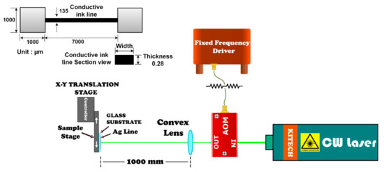
Figure 1.
Schematic diagram of the experimental setup for pulsed laser sintering of the Ag NPs conductive ink lines. The dimensions of the conductive ink line along with the pads printed on either side are depicted on the top left corner.
3. Numerical Calculations
A three-dimensional numerical calculation was carried out in COMSOL Multiphysics for thermal analysis of the pulsed laser sintering process of inkjet-printed Ag NPs lines on glass substrates. The two-dimensional cross-sectional schematic of the three-dimensional calculation model is presented in Figure 2. The three-dimensional model is depicted in Figure S2 (Supplementary Materials). The following assumptions were adopted for the calculation model. The absorbed laser energy was completely converted into heat and no phase change was considered for the Ag NPs because of the high melting temperatures of Ag NPs. Constant specific heat and density were adopted for Ag NPs. The initial condition was set at 20 °C. The convection and radiation boundary conditions were applied on the surface of the printed conductive ink line and the glass substrate in the form of external natural convection. The natural convection coefficient is expressed in Equation (S1) (Supplementary Materials).
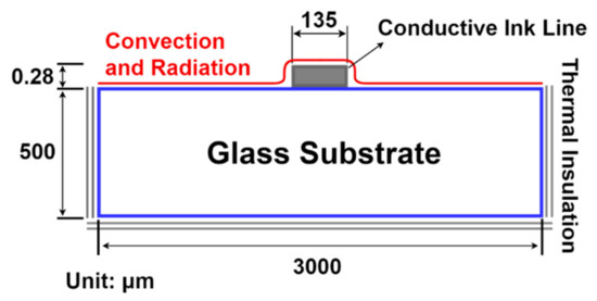
Figure 2.
Two-dimensional cross-sectional schematic of the three-dimensional model used for temperature calculation during the pulsed laser sintering of Ag NPs, where the two sides and the bottom surface of the glass substrate are thermally insulated and the top surface of the ink and the glass substrate is subjected to convection and radiation boundary conditions.
Thermal insulation was applied at the two sides and bottom part of the glass substrate, where the temperature gradient across these boundaries was zero. The pulsed laser sintering of Ag NPs lines inkjet-printed on glass substrates was analyzed by a transient three-dimensional heat conduction equation as follows:
where ρ, Cp, k, and u are density, specific heat capacity, thermal conductivity of the Ag NPs/glass substrate, and moving velocity of the laser beam, respectively. The subscript i = 1 and i = 2 represent Ag NPs and glass substrate, respectively (See Table 1). In addition, u1 is the scanning velocity of the laser beam and u2 is zero. The term Q1(t) is the laser heat source, which is given as follows:
where R(T), P, r, p(t), and γ are reflectivity, laser power, laser beam radius at 1/e2 of the Gaussian distribution, pulse time, and optical absorption length, respectively. The terms v, t, xfp, and yfp stand for speed of laser scanning speed, time after the start, and initial laser focal x, y-position at the start in terms of the peak of the Gaussian beam, respectively. The reflectivity and the absorption length at the laser wavelength were acquired experimentally. Figure S3 (Supplementary Materials) shows the plot for the normal reflectivity and absorption length of the incident laser beam against different sintering temperatures. The data used in these plots were calculated from the optical properties measured from ellipsometry [32]. To obtain the density of the printed Ag NPs lines, the porosity in the printed lines was considered and determined as 26% (the method has been described in the reference [33]). We assumed the empty space as air and the rest as Ag NPs. The density and heat capacity of the printed lines were determined to be 7762.6 kg/m3 and 245 J/(kg·K), respectively. The material properties of the glass substrate (Corning Eagle XG Slim glass, Samsung-Corning, Glendale, AZ, USA) were obtained from the product information sheet provided by the manufacturer.

Table 1.
Parameters used in the numerical calculations.
The thermal conductivity of Ag NPs is known as a function of the process temperature. Therefore, the temperature-dependent thermal conductivity of the Ag NPs obtained from reference [34] was considered in this study. During the pulsed laser sintering process, each pulse is followed by a relaxation period depending upon the pulse repetition rate. The maximum temperature rise is attained at the end of each laser pulse consequently inducing the Ag NPs thermal conductivity of sintered morphology. During the pulse relaxation period, the temperature drops, and an algorithm that can store the maximum temperature and the corresponding thermal conductivity by the previous laser shot as the initial condition for the following laser shot. As a result, the elevated thermal conductivity of the sintered zone was not decreased by the NPs cooled temperature during the pulse relaxation period.
A fine mesh system was chosen for the calculation model. The overall average mesh quality was 0.903. The one is the best possible quality value in the software. During the simulation, shorter time steps played a significant role in producing precise results and avoiding any discontinuity within the calculation period. Therefore, keeping the computation time to a minimum, a time-step of 5 ms was chosen as the upper limit. The parametric values adopted in the numerical model are listed in Table 1.
4. Results and Discussion
Ag NPs printed lines were sintered to find the effect of laser parameters on the surface morphology and electrical properties. Beam duration of a CW laser was modulated into milliseconds and microseconds with appropriate repetition rates. In Figure 3 the resistivities of Ag NPs lines are presented with various scanning speeds of 14, 27, 81, 135, and 189 μm/s. The pulse durations of 10 and 100 ms with corresponding repetition rates of 10 and 1 Hz at 276 mW were tested to find the combinations that can produce low Ag NPs line resistivity. A minimum resistivity of about 3 μΩ·cm was obtained with 100 ms and 1 Hz at the scanning speed of 135 μm/s, which corresponded to 50% of pulse overlapping. With 95% overlapping at 14 μm/s with 100 ms and 1 Hz, the resistivity of approximately 3.7 μΩ·cm was obtained. However, 95% overlapping at 14 μm/s is impractical to be applied since the total scanning times reaches to 500 s to cover the 7 mm-long sample. The laser parameters of 100 ms, 1 Hz, and 135 μm/s were adopted for the numerical calculation since the lowest resistivity was obtained at this combination.
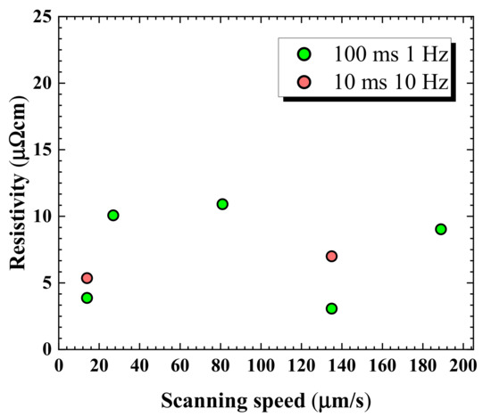
Figure 3.
Resistivity against various scanning speeds for 100 ms and 10 ms pulse durations at 1 Hz and 10 Hz repetition rates.
The obtained minimum resistivity is an improved result compared with those from previous laser sintering studies [35] and conventional oven sintering at much higher temperatures and longer processing times [36,37]. Using similar Ag NPs ink composition, Moon et al. [38] were able to produce 5.8 μΩ·cm via furnace sintering at 250 °C for 30 min. Moreover, the obtained minimum resistivity of approximately 3 μΩ·cm with 100 ms, and laser parameters of 1 Hz, 276 mW, and 135 μm/s is lower than the reported values from several other sintering methods [18,39]. The discrepancies among the resistivity values in Figure 3 have been found to be caused by several parameters such as surface morphology [40], laser wavelength effect [35,40], properties of the organic additives used in the NPs ink [16,41], the size of NPs [36,42], laser power, and scanning speed [14,35,43].
The periodic temperature fluctuations caused by the pulse interaction and relaxation periods are depicted in Figure 4. The position where the maximum temperature appears coincides with the center of the irradiated laser beam at the specified moment. The 7000 μm-long Ag NPs line is completely covered in approximately 52 s with a scanning speed of 135 μm/s. The maximum recorded temperature was around 204.4 °C. As mentioned before, 5.8 μΩ·cm were obtained via furnace sintering at 250 °C for 30 min. However, the lower resistivity of 3 μΩ·cm was produced at 204.4 °C in scanning pulsed laser sintering. The drop in the temperature profile after attaining the maximum local temperature at the end of each pulse is due to the pulse relaxation (0.9 s pulse relaxation period). During the laser interaction period of 0.1 s, the energy is absorbed by the NPs and subsequently conducted to the surrounding NPs. The laser energy absorption and the subsequent heat loss from the NPs to their surroundings occur in less than 1 ns [44,45]. Therefore, the 0.1 s laser beam interaction period with the Ag NPs is long enough to cause a continuous rise in the process temperature. The rise and fall of the temperature in the plot depict the corresponding laser excitation and relaxation periods. During the simulation, the starting position of the laser scan was at the boundary of the Ag NPs pad and Ag NPs line such that half of the laser beam irradiated on the pad and half on the Ag NPs line. From the plot we notice that the temperature rise is instantaneous as the pulse interacts with the NPs without any time delay. However, the maximum temperature is attained after the laser irradiation of 0.1 s. As soon as the pulse is relaxed (no heat source) the underlying NPs start to cool, and it takes 0.905 s (0.9 s of no heat source and 5 ms of step time delay) to reach to near room temperature until the next pulse hits. For the first laser pulse in Figure 4, the temperature in the underlying Ag NPs layer increases and the Ag NPs layer is thermally sintered, subsequently, increasing the corresponding thermal conductivity of the Ag NPs. In the following pulse relaxation period, the process temperature drops, and the thermal conductivity of the heated zone is initialized with the value of the corresponding maximum temperature induced in the previous laser shot. The plot shows that a peak temperature of about 204 °C is obtained at around 52 s. The peak temperature of around 207 °C produced by the first pulse is slightly higher than the following peak temperature of about 201 °C. The slightly lower following peak temperature of 201 °C is due to the absorption into 50 % of the already irradiated area. As a result, half of the laser irradiation is absorbed by the area with high thermal conductivity. This resulted from the high thermal diffusivity which was caused by a slightly higher temperature from the previous laser pulse.
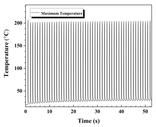
Figure 4.
Maximum temperature profile after a full pulsed laser scan over the printed Ag NP line. The maximum recorded temperature was approximately 204.4 °C. The full laser scan across the entire 7000 μm length of the printed Ag NPs line takes around 52 s at a scanning speed of 135 μm/s.
Typically, the heat relaxation time depends upon thermal diffusivity caused from the increase in thermal conductivity and the decrease in heat capacitance. The abrupt cooling rate within the initial time step after the peak temperature and the relatively moderate cooling rates afterward, can be elaborated by the 2D surface plots as shown in Figure 5. The time steps and the cooling rates for Figure 5 are extracted from Figure 4. The reason for an abrupt cooling rate is due to the relatively small heat capacitance of silver nanoparticles (bulk Ag, cp = 245 J/kg·K [34]) adopted in this study and high thermal conductivity induced after the laser shot. The thermal conductivity of the glass substrate was known to be very low at 1.05 W/m·K, which could not effectively act as a heat sink to help a faster heat relaxation in the Ag NPs layer [46,47]. Therefore, the cooling via radiative and convective cooling might be responsible for this fast cooling rate.
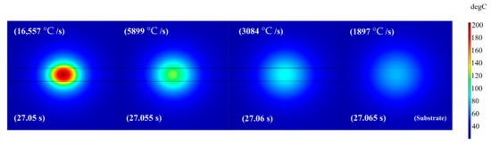
Figure 5.
2D surface plots show the temperature distribution at different time steps. The first 5 ms after the peak temperature shows high cooling rate while the cooling rates reduces as the time steps progresses.
In Figure 6, the transient temperature behavior is depicted at a single point graph in which a local maximum temperature is recorded at 27.05 s (at the center of the laser beam). The previous temperature peaks appeared from the effect of previous laser pulses at this point. The temperature history depicts that the previous laser beams have caused the peaks at 26.05 s, 25.05 s, etc., and the peaks after 27.05 s are affected by the subsequent laser beams. The corresponding maximum temperatures (Tmax) from the previous laser shots, are stored for determining the corresponding thermal conductivity values for the next temperature calculation. After 27.05 s the maximum temperature is fixed at 204 °C, hence the corresponding thermal conductivity is maintained in spite of the reduction in temperature. The effect of higher thermal conductivity becomes immediately observable after the 27.05 s. The peak at 28.05 s is shorter than the peak at 26.05 s. The temperature at 26.05 s is approximately 117 °C while that at 28.05 s is approximately 105 °C.
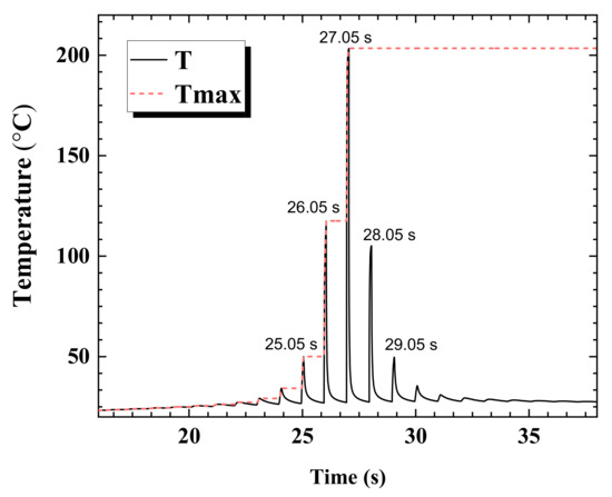
Figure 6.
The transient behavior of T (temperature) and Tmax (stored maximum temperature) plotted at a point where the maximum temperature is recorded at 27.05 s.
In Figure 7, the spatial distributions of thermal conductivity are presented at three points located in the start, middle, and the end of the printed line. Due to the nature of the Gaussian beam, a decrease in the temperature was witnessed away from the center of the beam [48]. At the start of the silver line, maximum value of about 44 W/(m·K) is recorded against the maximum temperature of 201 °C. Furthermore, as we progress, the conductivity of 46 W/(m·K) value is recorded against 203 °C at the middle of the line, and, finally, the conductivity of 49 W/(m·K) value against 204.4 °C.
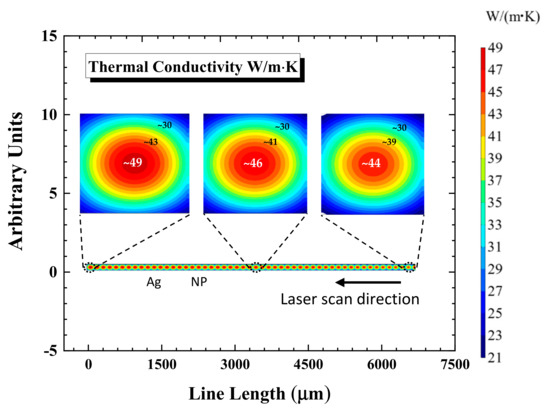
Figure 7.
Spatial thermal conductivity distributions are presented at the start, middle, and end throughout the sintered NP line. The magnified areas are highlighted the thermal conductivity distribution at different points.
The reason behind the slightly increasing temperature trend in Figure 4 can be elaborated by considering the “residual temperature”. It is defined as an initial temperature just before the start of next laser pulse [20]. Figure 8 presents the residual temperatures after a complete laser scan of the entire 7000 μm-long printed conductive line, which are extracted from transient temperature variations in Figure 4. The region away from the domain hit by a laser pulse does not cool to room temperature before the next pulse is hit. To understand this, we calculated the thermal diffusion length induced by the pulsed laser operation to show how far the heat diffuses after a laser shot. For the current pulsed laser process configuration, the thermal diffusion length is roughly estimated by the following relation.
where dL, α, and τ, stand for thermal diffusion length, thermal diffusivity, and pulse duration, respectively. The thermal diffusivity is obtained from the Ag NPs thermal conductivity of 49 W/m·K, density 7762.6 kg/m3, and heat capacity 245 J/kg·K values. With a pulse duration of 100 ms, the calculated heat diffusion length is approximately 3.2 mm, which is much larger than the beam diameter of 270.9 μm. Therefore, the region ahead of the laser irradiation area is thermally affected before the irradiation of the scanning laser beam. The residual temperature increases with the progressing pulse train. The pulse repetition rate provides a shorter thermal relaxation period than the time needed for the Ag NPs to cool off completely to room temperature (Ti = 20 °C). This behavior indicates that a residual temperature acts as an initial condition for the following laser pulse. Consequently, the attained higher peak temperature cools to slightly higher residual temperature with each progressing laser pulse. High residual temperatures can be detrimental to the underlying substrate because it increases the overall process temperature and heating duration.
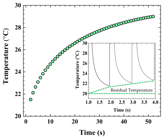
Figure 8.
The residual temperature profile was extracted from Figure 4. The inset shows a magnified residual temperature curve from the temperature profile.
Furthermore, Equation (3) tells us that a longer pulse duration will cause a wider thermal diffusion length. The reason is that a longer pulse duration supplies prolonged thermal energy to the underlying NPs providing enough time for the wider propagation of heat as reported in a previous study [26]. The vertically deeper heat diffusion length is known to cause complete sintering which tends to increase the possibility of the adhesion strength between the NPs layer and the underlying substrate [26,40,49]. Figure 9 presents the residual temperature plots under the varied experimental parameters. The corresponding maximum temperature plots are presented in Figure S4 (Supplementary Materials). The laser power for each case was adjusted such that each case produced almost similar temperatures at the start of the laser scan. The cases shown in Figure 9a–c,e have the same scanning speed, while the scanning speed of the cases shown in Figure 9a,d,f were chosen so that the cases have the same pulse overlap. For the thermal diffusion lengths of 100, 10, and 1 ms through the glass substrate are calculated to be 438.5 μm, 138.6 μm, and 43.8 μm, respectively. These values suggest that longer pulse durations affect the substrate to a comparatively higher degree.
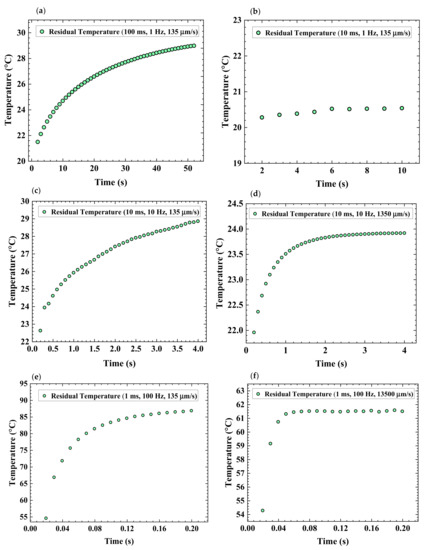
Figure 9.
Effect of pulse duration, repetition rates, and scanning speed on residual temperatures (a) 100 ms, 1 Hz, 135 μm/s, and 276 mW, (b) 100 ms 1 Hz, 135 μm/s, and 276 mW, (c) 10 ms, 10 Hz, 135 μm/s, and 0.42 mW, (d) 10 ms, 10 Hz, 1350 μm/s, and 0.42 mW, (e) 1 ms, 100 Hz, 135 μm/s, and 1.7 W, (f) 10 ms, 10 Hz, 135 μm/s, and 1.7 W. Different powers were chosen for each case to achieve similar to starting temperature with 100 ms. The thermal diffusion length through the glass substrate for 1 ms pulse duration is calculated to be 43.8 μm.
Figure 10a,c show the temperature distribution of heat-affected zones in the vertical direction and on the surface of the glass substrate at 51.05 s. The temperature distributions are recorded at the end point of the Ag NPs line where the peak temperature of approximately 204 °C occurred at the center of the irradiated beam profile. Figure 10b depicts the temperature curve along the broken line into the glass substrate as shown in Figure 10a. In Figure 10d the profiles of the temperature distribution along the broken line in Figure 10c resemble a Gaussian profile of a laser beam. The thin solid lines in Figure 10c are the printed Ag NPs line and the pad. The temperature at the edge of the Ag NPs line is around 162 °C and is further reduced as the distance is increased away from the beam center. These estimated temperatures are allowable for the flexible polyimide (PI) substrates which have a glass transition temperature of around 385 °C during thermal sintering [18,42].
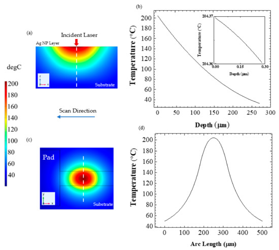
Figure 10.
(a) Cross-sectional temperature distribution at 51.05 s is illustrated. The white dashed line represents the depth. (b) Temperature profile is shown with respect to depth through the printed Ag NP line and the glass substrate. The inset shows the temperature distribution in the Ag NP layer. (c) Top surface temperature distribution at 51.05 s is illustrated by the incident laser on the Ag NP line. The white dashed line represents the arc length. (d) Temperature profile is presented with respect to the arc length.
5. Conclusions
In this contribution, pulsed laser sintering of inkjet-printed Ag NPs lines was conducted. Using the laser power with 276 mW laser power, 100 ms pulse duration, and 1 Hz repetition rate at a scanning speed of 135 μm/s, a very low Ag NPs resistivity of approximately 3 μΩ·cm within 52 s was obtained, which is 1.9 times the bulk Ag resistivity (1.6 μΩ). For accurate temperature calculation during pulsed laser sintering of Ag NPs, a numerical model was developed. Our unique algorithm enabled us to store the maximum temperature induced by the previous laser shot avoiding the thermal conductivity drop during the pulse relaxation period. By storing the maximum temperature, the corresponding thermal conductivity value could be stored, which was adopted as an initial condition for the following laser shots. We elaborated on the effects of pulse duration, repetition rates, and scanning speeds on the residual temperature and thermal diffusion length. While longer pulse durations cause longer thermal diffusion lengths, the higher repetition rates produce higher residual temperatures, which can be controlled by increasing the scanning speed.
Supplementary Materials
The following are available online at https://www.mdpi.com/article/10.3390/app12073467/s1, Equation (S1): Convection heat transfer coefficient h used in the numerical model, where, k, L, and RaL are thermal conductivity, characteristic length, and Rayleigh number, respectively, Figure S1: Illustration of a Gaussian beam profile which depicts the chosen beam diameter (270.9 μm) selected for the pulsed laser operation in comparison to the printed Ag NPs line width of 135 μm, Figure S2: 3-D model used for the temperature estimation during pulsed laser sintering of inkjet-printed Ag NP line on a glass substrate, Figure S3: Normal reflectivity and absorption length of Ag NPs structures measured by ellipsometry at different sintering temperature, Figure S4: Maximum temperature plots for (a) 100 ms, 1 Hz, 135 μm/s, 276 mW (b) 10 ms 1 Hz and 135 μm/s, 276 mW. (c) 10 ms, 10 Hz, 135 μm/s and 420 mW (d) 10 ms, 10 Hz, 1350 μm/s and 420 mW (e) 1 ms, 100 Hz, 135 μm/s and 1.7 W (f) 1 ms, 100 Hz, 13500 μm/s and 1.7 W.
Author Contributions
Conceptualization, S.-J.M. and A.H.; methodology, Y.-J.M. and H.-L.L.; software, A.H.; validation, H.-L.L.; formal analysis, A.H. and H.-L.L.; investigation, A.H.; resources, J.-Y.H. and H.K.; data curation, A.H.; writing—original draft preparation, A.H.; writing—review and editing, S.-J.M.; supervision, S.-J.M.; project administration, S.-J.M.; funding acquisition, H.K. All authors have read and agreed to the published version of the manuscript.
Funding
This study was conducted with the support of the Korea Institute of Industrial Technology as “Development of root technology for multi-product flexible production” (KITECH EO-22-0006).
Acknowledgments
We would like to thank the Higher Education Commission of Pakistan for financial support to Arif Hussain.
Conflicts of Interest
The authors declare no conflict of interest.
References
- Ross, I.M. The invention of the transistor. Proc. IEEE 1998, 86, 7–28. [Google Scholar] [CrossRef]
- Khan, Y.; Thielens, A.; Muin, S.; Ting, J.; Baumbauer, C.; Arias, A.C. A New Frontier of Printed Electronics: Flexible Hybrid Electronics. Adv. Mater. 2020, 32, 1905279. [Google Scholar] [CrossRef] [PubMed]
- Chelton, C.F.; Glowatz, M.; Mosovsky, J.A. Chemical Hazards in the Semiconductor Industry. IEEE Trans. Educ. 1991, 34, 269–288. [Google Scholar] [CrossRef]
- Park, D.-U.; Byun, H.-J.; Choi, S.-J.; Jeong, J.-Y.; Yoon, C.-S.; Kim, C.-N.; Ha, K.-C.; Park, D.-Y. Review on Potential Risk Factors in Wafer Fabrication Process of Semiconductor Industry. Korean J. Occup. Environ. Med. 2011, 23, 333–342. [Google Scholar] [CrossRef]
- Umar, K.; Yaqoob, A.A.; Ibrahim, M.N.M.; Parveen, T.; Safian, M.T. Environmental applications of smart polymer composites. In Smart Polymer Nanocomposites; Woodhead Publishing: Sawston, UK, 2021; pp. 295–312. [Google Scholar] [CrossRef]
- Sowade, E.; Kang, H.; Mitra, K.Y.; Weiß, O.J.; Weber, J.; Baumann, R.R. Roll-to-roll infrared (IR) drying and sintering of an inkjet-printed silver nanoparticle ink within 1 second. J. Mater. Chem. C 2015, 3, 11815–11826. [Google Scholar] [CrossRef]
- Zhong, Z.; Ko, P.; Seok, J.Y.; Kim, H.; Kwon, S.; Youn, H.; Woo, K. Roll-to-Roll Reverse-Offset Printing Combined with Photonic Sintering Process for Highly Conductive Ultrafine Patterns. Adv. Eng. Mater. 2020, 22, 2000463. [Google Scholar] [CrossRef]
- Balliu, E.; Andersson, H.; Engholm, M.; Öhlund, T.; Nilsson, H.E.; Olin, H. Selective laser sintering of inkjet-printed silver nanoparticle inks on paper substrates to achieve highly conductive patterns. Sci. Rep. 2018, 8, 1–9. [Google Scholar] [CrossRef]
- Kim, Y.H.; Heo, J.S.; Kim, T.H.; Park, S.; Yoon, M.H.; Kim, J.; Oh, M.S.; Yi, G.R.; Noh, Y.Y.; Park, S.K. Flexible metal-oxide devices made by room-temperature photochemical activation of sol-gel films. Nature 2012, 489, 128–132. [Google Scholar] [CrossRef]
- Son, Y.; Yeo, J.; Moon, H.; Lim, T.W.; Hong, S.; Nam, K.H.; Yoo, S.; Grigoropoulos, C.P.; Yang, D.Y.; Ko, S.H. Nanoscale electronics: Digital fabrication by direct femtosecond laser processing of metal nanoparticles. Adv. Mater. 2011, 23, 3176–3181. [Google Scholar] [CrossRef]
- Kant, T.; Shrivas, K.; Tapadia, K.; Devi, R.; Ganesan, V.; Deb, M.K. Inkjet-printed paper-based electrochemical sensor with gold nano-ink for detection of glucose in blood serum. New J. Chem. 2021, 45, 8297–8305. [Google Scholar] [CrossRef]
- Bao, Z.; Chen, X.; Bao, Z.; Chen, X. Flexible and Stretchable Devices. J. Electr. Electron. Syst. 2016, 28, 4177–4179. [Google Scholar] [CrossRef] [PubMed] [Green Version]
- Wang, Y.H.; Du, D.X.; Xie, H.; Zhang, X.B.; Lin, K.W.; Wang, K.; Fu, E. Printability and electrical conductivity of silver nanoparticle-based conductive inks for inkjet printing. J. Mater. Sci. Mater. Electron. 2021, 32, 496–508. [Google Scholar] [CrossRef]
- Zenou, M.; Ermak, O.; Saar, A.; Kotler, Z. Laser sintering of copper nanoparticles. J. Phys. D Appl. Phys. 2014, 47, 025501. [Google Scholar] [CrossRef]
- Ko, S.H.; Pan, H.; Grigoropoulos, C.P.; Luscombe, C.K.; Fréchet, J.M.J.; Poulikakos, D. All-inkjet-printed flexible electronics fabrication on a polymer substrate by low-temperature high-resolution selective laser sintering of metal nanoparticles. Nanotechnology 2007, 18, 345202. [Google Scholar] [CrossRef]
- Szczech, J.B.; Megaridis, C.M.; Gamota, D.R.; Zhang, J. Fine-line conductor manufacturing using drop-on-demand PZT printing technology. IEEE Trans. Electron. Packag. Manuf. 2002, 25, 26–33. [Google Scholar] [CrossRef]
- Allen, M.L.; Aronniemi, M.; Mattila, T.; Alastalo, A.; Ojanperä, K.; Suhonen, M.; Seppä, H. Electrical sintering of nanoparticle structures. Nanotechnology 2008, 19, 175201. [Google Scholar] [CrossRef]
- Perelaer, J.; De Gans, B.J.; Schubert, U.S. Ink-jet printing and microwave sintering of conductive silver tracks. Adv. Mater. 2006, 18, 2101–2104. [Google Scholar] [CrossRef]
- Kang, H.; Sowade, E.; Baumann, R.R. Direct intense pulsed light sintering of inkjet-printed copper oxide layers within six milliseconds. ACS Appl. Mater. Interfaces 2014, 6, 1682–1687. [Google Scholar] [CrossRef]
- Bolduc, M.; Trudeau, C.; Beaupré, P.; Cloutier, S.G.; Galarneau, P. Thermal Dynamics Effects using Pulse-Shaping Laser Sintering of Printed Silver Inks. Sci. Rep. 2018, 8, 1418. [Google Scholar] [CrossRef] [Green Version]
- Khabarov, K.; Kornyushin, D.; Masnaviev, B.; Tuzhilin, D.; Saprykin, D.; Efimov, A.; Ivanov, V. The influence of laser sintering modes on the conductivity and microstructure of silver nanoparticle arrays formed by dry aerosol printing. Appl. Sci. 2020, 10, 246. [Google Scholar] [CrossRef] [Green Version]
- Son, Y.; Yeo, J.; Ha, C.W.; Lee, J.; Hong, S.; Nam, K.H.; Yang, D.Y.; Ko, S.H. Application of the specific thermal properties of Ag nanoparticles to high-resolution metal patterning. Thermochim. Acta 2012, 542, 52–56. [Google Scholar] [CrossRef]
- Yaqoob, A.A.; Umar, K.; Ibrahim, M.N.M. Silver nanoparticles: Various methods of synthesis, size affecting factors and their potential applications—A review. Appl. Nanosci. 2020, 10, 1369–1378. [Google Scholar] [CrossRef]
- Zacharatos, F.; Theodorakos, I.; Karvounis, P.; Tuohy, S.; Braz, N.; Melamed, S.; Kabla, A.; de la Vega, F.; Andritsos, K.; Hatziapostolou, A.; et al. Selective laser sintering of laser printed Ag nanoparticle micropatterns at high repetition rates. Materials 2018, 11, 2142. [Google Scholar] [CrossRef] [PubMed] [Green Version]
- Peng, P.; Hu, A.; Zhou, Y. Laser sintering of silver nanoparticle thin films: Microstructure and optical properties. Appl. Phys. A 2012, 108, 685–691. [Google Scholar] [CrossRef]
- Yang, G.; Xu, G.; Li, Q.; Zeng, Y.; Zhang, Y.; Hao, M.; Cui, C. Understanding the sintering and heat dissipation behaviours of Cu nanoparticles during low-temperature selective laser sintering process on flexible substrates. J. Phys. D Appl. Phys. 2021, 54, 375304. [Google Scholar] [CrossRef]
- Asoro, M.; Kovar, D.; Damiano, J.; Ferreira, P. Scale Effects on the Melting Behavior of Silver Nanoparticles. Microsc. Microanal. 1976, 13, 1802–1803. [Google Scholar] [CrossRef] [Green Version]
- Luo, W.; Hu, W.; Xiao, S. Size effect on the thermodynamic properties of silver nanoparticles. J. Phys. Chem. C 2008, 112, 2359–2369. [Google Scholar] [CrossRef]
- Buffat, P.; Borel, J.P. Size effect on the melting temperature of gold particles. Phys. Rev. A 1976, 13, 2287–2298. [Google Scholar] [CrossRef] [Green Version]
- Yang, C.C.; Li, S. Investigation of cohesive energy effects on size-dependent physical and chemical properties of nanocrystals. Phys. Rev. B Condens. Matter Mater. Phys. 2007, 75, 165413. [Google Scholar] [CrossRef]
- Ko, S.H.; Pan, H.; Grigoropoulos, C.P.; Luscombe, C.K.; Fráchet, J.M.J.; Poulikakos, D. Air stable high resolution organic transistors by selective laser sintering of ink-jet printed metal nanoparticles. Appl. Phys. Lett. 2007, 90, 141103. [Google Scholar] [CrossRef] [Green Version]
- Modest, M.F. The Interface Between a Perfect Dielectric and Absorbing Medium. In Radiative Heat Transfer; Modest, M.F., Ed.; Academic Press: Cambridge, MA, USA, 2013; pp. 50–53. [Google Scholar]
- Tadjiki, S.; Montaño, M.D.; Assemi, S.; Barber, A.; Ranville, J.; Beckett, R. Measurement of the Density of Engineered Silver Nanoparticles Using Centrifugal FFF-TEM and Single Particle ICP-MS. Anal. Chem. 2017, 89, 6056–6064. [Google Scholar] [CrossRef] [PubMed]
- Choi, J.H.; Ryu, K.; Park, K.; Moon, S.J. Thermal conductivity estimation of inkjet-printed silver nanoparticle ink during continuous wave laser sintering. Int. J. Heat Mass Transf. 2015, 85, 904–909. [Google Scholar] [CrossRef]
- Kang, B.; Ko, S.; Kim, J.; Yang, M. Microelectrode fabrication by laser direct curing of tiny nanoparticle self-generated from organometallic ink. Opt. Express 2011, 19, 2573. [Google Scholar] [CrossRef] [PubMed]
- Perelaer, J.; De Laat, A.W.M.; Hendriks, C.E.; Schubert, U.S. Inkjet-printed silver tracks: Low temperature curing and thermal stability investigation. J. Mater. Chem. 2008, 18, 3209–3215. [Google Scholar] [CrossRef]
- Halonen, E.; Viiru, T.; Östman, K.; Cabezas, A.L.; Mantysalo, M. Oven sintering process optimization for inkjet-printed Ag Nanoparticle ink. IEEE Trans. Compon. Packag. Manuf. Technol. 2013, 3, 350–356. [Google Scholar] [CrossRef]
- Moon, Y.J.; Kang, H.; Kang, K.; Moon, S.J.; Young Hwang, J. Effect of Thickness on Surface Morphology of Silver Nanoparticle Layer During Furnace Sintering. J. Electron. Mater. 2015, 44, 1192–1199. [Google Scholar] [CrossRef]
- Tobjörk, D.; Aarnio, H.; Pulkkinen, P.; Bollström, R.; Määttänen, A.; Ihalainen, P.; Mäkelä, T.; Peltonen, J.; Toivakka, M.; Tenhu, H.; et al. IR-sintering of ink-jet printed metal-nanoparticles on paper. Thin Solid Film. 2012, 520, 2949–2955. [Google Scholar] [CrossRef]
- Paeng, D.; Yeo, J.; Lee, D.; Moon, S.J.; Grigoropoulos, C.P. Laser wavelength effect on laser-induced photo-thermal sintering of silver nanoparticles. Appl. Phys. A Mater. Sci. Process. 2015, 120, 1229–1240. [Google Scholar] [CrossRef]
- Szczech, J.B.; Megaridis, C.M.; Zhang, J.; Gamota, D.R. Ink jet processing of metallic nanoparticle suspensions for electronic circuitry fabrication. Microscale Thermophys. Eng. 2004, 8, 327–339. [Google Scholar] [CrossRef]
- Kim, D.; Moon, J. Highly Conductive Ink Jet Printed Films of Nanosilver Particles for Printable Electronics. Electrochem. Solid-State Lett. 2005, 8, J30–J33. [Google Scholar] [CrossRef]
- Yu, J.H.; Jung, H.S.; Jeong, J.K.; Kang, K.-T. Sintering Behavior of Copper Nanoparticle Ink by Laser in Air. J. Nanosci. Nanotechnol. 2018, 19, 1261–1268. [Google Scholar] [CrossRef] [PubMed]
- Ekici, O.; Harrison, R.K.; Durr, N.J.; Eversole, D.S.; Lee, M.; Ben-Yakar, A. Thermal analysis of gold nanorods heated with femtosecond laser pulses. J. Phys. D. Appl. Phys. 2008, 41, 185501. [Google Scholar] [CrossRef] [PubMed]
- Yao, Y.L.; Chen, H.; Zhang, W. Time scale effects in laser material removal: A review. Int. J. Adv. Manuf. Technol. 2005, 26, 598–608. [Google Scholar] [CrossRef]
- Hernandez-Castaneda, J.C.; Lok, B.K.; Zheng, H. Laser sintering of Cu nanoparticles on PET polymer substrate for printed electronics at different wavelengths and process conditions. Front. Mech. Eng. 2020, 15, 303–318. [Google Scholar] [CrossRef]
- Kumpulainen, T.; Pekkanen, J.; Valkama, J.; Laakso, J.; Tuokko, R.; Mäntysalo, M. Low temperature nanoparticle sintering with continuous wave and pulse lasers. Opt. Laser Technol. 2011, 43, 570–576. [Google Scholar] [CrossRef]
- Bieri, N.R.; Chung, J.; Poulikakos, D.; Grigoropoulos, C.P. Manufacturing of nanoscale thickness gold lines by laser curing of a discretely deposited nanoparticle suspension. Superlattices Microstruct. 2004, 35, 437–444. [Google Scholar] [CrossRef]
- Ermak, O.; Zenou, M.; Toker, G.B.; Ankri, J.; Shacham-Diamand, Y.; Kotler, Z. Rapid laser sintering of metal nano-particles inks. Nanotechnology 2016, 27, 385201. [Google Scholar] [CrossRef]
Publisher’s Note: MDPI stays neutral with regard to jurisdictional claims in published maps and institutional affiliations. |
© 2022 by the authors. Licensee MDPI, Basel, Switzerland. This article is an open access article distributed under the terms and conditions of the Creative Commons Attribution (CC BY) license (https://creativecommons.org/licenses/by/4.0/).