Communication

Wideband Three-Dimensional Absorber Based on Notch-Slot Resonator with Lossy Coupled Microstrip Line

1
School of Information and Electrical Engineering, Zhejiang University City College, Hangzhou 310015, China
2
Key Laboratory of RF Circuits & System of Ministry of Education, School of Electronics and Information, Hangzhou Dianzi University, Hangzhou 310018, China
3
Shanghai Huawei Technologies Co., Ltd., Shanghai 201206, China
*
Author to whom correspondence should be addressed.
Appl. Sci. 2022, 12(21), 11082; https://doi.org/10.3390/app122111082
Submission received: 28 September 2022 / Revised: 31 October 2022 / Accepted: 31 October 2022 / Published: 1 November 2022

Abstract

:
A wideband three-dimensional (3D) absorber based on a notch-slot resonator is proposed in this paper. A lossy coupled microstrip line was applied to eliminate the reflection band of the original lossy notch-slot resonator, resulting in a wide absorption band. A single-polarized design was first proposed, and the operating principle was demonstrated. Then, a dual-polarized design was presented, fabricated and measured. To eliminate the undesirable resonances caused by the securing slits cut between the two adjacent unit cells, some shorting pins were introduced. The measured results show that the dual-polarized absorber exhibits an absorption band from 2.74 GHz to 11.08 GHz (120.69% fractional bandwidth), and it is also stable under the incident angles up to 40° for both TE and TM polarizations.

1. Introduction

Microwave absorbers have been intensively studied over the decades due to their wide civil and military applications such as electromagnetic compatibility (EMC) and radar cross-section (RCS) reduction. A Salisbury screen [1] is a simple and classic absorber, which consists of a resistive sheet and conducting plate with a distance of a quarter-wavelength. The absorption band of a Salisbury screen is relatively narrow because of its single resonance. Using two or more resistive layers, a Jaumann absorber [2,3] features a wider absorption band at the expense of large thickness. A circuit analog (CA) absorber [3,4,5,6,7], which can be modeled as a series RLC resonator, was developed to increase the absorption band and reduce the thickness. In [4], a CA absorber consisting of double-square loop unit cells achieves a 128% fractional bandwidth (FBW) with a small thickness of 0.088λL. (λL is the free-space wavelength of the lowest frequency of the absorption band). Metamaterial absorbers [8,9,10] are another kind of absorber that can achieve efficient and broadband absorption without lumped resistors. In [10], by deliberately controlling multiple resistive electric and magnetic resonances in terms of dispersion and dissipation, an absorption band of 48.6% FBW is obtained at the incident angle of 50°.
Recently, three-dimensional (3D) absorbers [11,12,13,14] have also been developed based on 3D frequency selective structures (FSSs). A wide absorption band can be obtained by merging the adjacent resonant modes of the multimode cavity of the 3D structure without increasing its thickness. In [12], a wideband absorber with a 148% FBW is proposed based on double-sided parallel-strip line resonators. The thickness of the absorber is only 0.1λL. However, the disadvantage of 3D absorbers is their complicated topology and large assembly tolerance. A new class of 3D FSSs and absorbers based on planar slotline resonators was proposed in [15,16]. The fabrication of planar slotline resonators is easy due to the planar topology. In [16], the planar slotline loaded with a resistor produces two absorption bands corresponding to its fundamental and first hormonic resonance. However, the absorption bands are relatively narrow (47.15% and 17.39% FBW).
In this paper, a 3D absorber utilizing a new lossy notch-slot resonator is proposed. Inspired by the coupled-feed wideband slot antennas [17,18], the lossy notch-slot resonator was implemented using a coupled microstrip line loaded with a resistor, instead of directly loading the resistor at the open end of the notch slot [16]. The incident EM waves were first coupled into the notch slot, then coupled to the microstrip line and finally, absorbed by the resistor. This method eliminates the reflection band of the original lossy notch-slot resonator and merges the fundamental and third-order resonances, resulting in an ultrawide absorption band. Both the single- and the dual-polarized designs are presented, and the dual-polarized one has been fabricated and measured and exhibits a wide absorption band from 2.74 GHz to 11.08 GHz (120.7% FBW). In addition, the proposed 3D absorber has a robust structure which is easy to fabricate compared to conventional 3D absorbers.

2. Single-Polarized 3D Absorber

2.1. Unit Cell Structure

The unit cell structure of the proposed single-polarized 3D absorber is shown in Figure 1. It is composed of a notch-slot resonator, a coupled U-shaped microstrip line and a reflecting plate, whose period is Lp × Lp along the x- and y-directions. The notch slot is printed on one side of the Rogers RO4350B substrate with a permittivity of 3.48 and a loss tangent of 0.001, while the coupled microstrip line is on the other side. The z-oriented parts of the coupled microstrip line are open-ended, and the y-oriented part is embedded with a chip resistor with a resistance of R in the center.
The parameters in Figure 1 are as follows: Lp = 11.0 mm, t = 0.8 mm, L = 18.0 mm, Ls = 15.0 mm, Ws = 5.5 mm, Lend = 1.0 mm, Wend = 2.5 mm, Wm = 1.0 mm, Lm1 = 5.4 mm, Lm2 = 9.0 mm, h = 6.0 mm and R = 200 Ω.

2.2. Operating Principle

The proposed absorber evolves from the original lossy slot resonator in [16]. Instead of directly loading the resistor at the open end of the notch slot, a microstrip line on the other side of the substrate is utilized to couple the energy from the notch slot to the microstrip line. When the incident TE-polarized EM wave strikes the proposed absorber, the energy is first coupled into the notch-slot resonator, exciting the y-oriented electric field in the slot. The current along the y-oriented microstrip line across the slot is then generated and absorbed by the loaded resistor. It is defined that the TE- and TM-polarized waves are with the E-field along the directions of the y- and x-axes, respectively. It is worth mentioning that the coupled microstrip line is inspired by the typical wideband slot antennas [17,18] fed by a microstrip line, and therefore it has a similar operating principle.
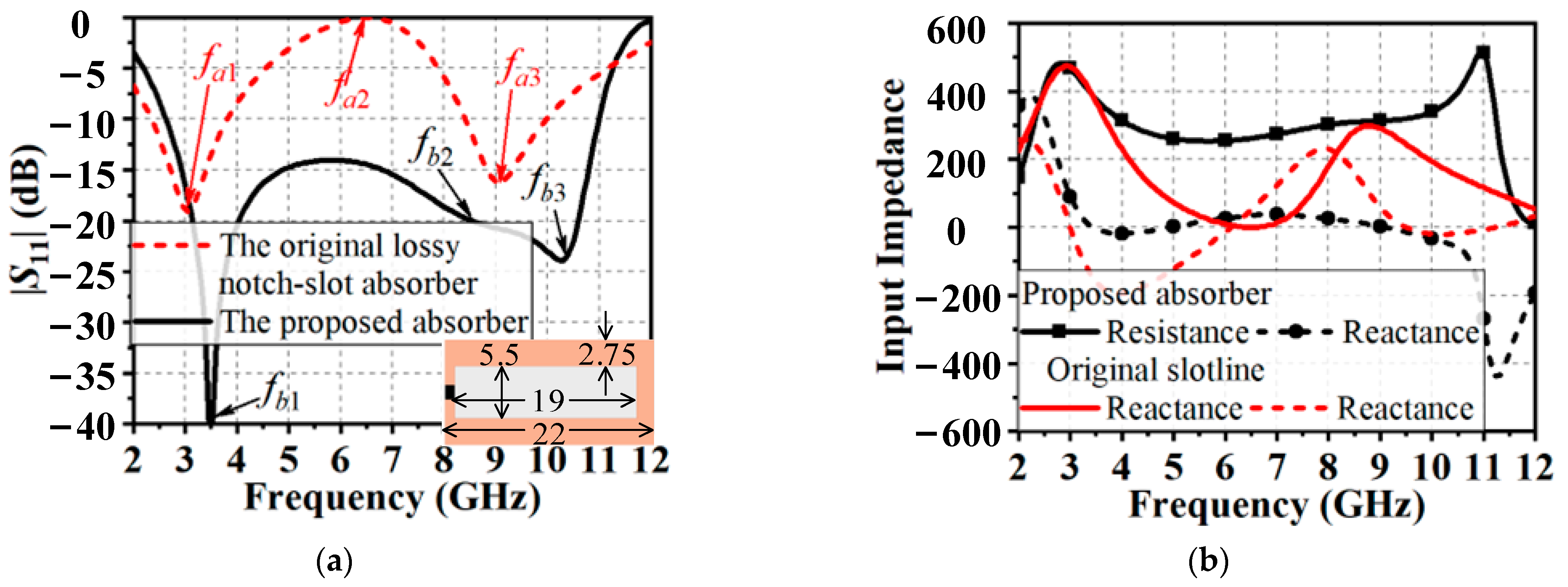
The proposed single-polarized 3D absorber is simulated using a high frequency structure simulator (HFSS) 15.0. It is noted that the absorption band is defined with |S11| ≤ −10 dB or absorption ≥ 90%. Figure 2a shows the |S11| of the proposed 3D absorber, and the |S11| of the original lossy notch-slot absorber with a resistor loaded at the open end (see the inset of Figure 2a) is also shown for comparison. It can be seen that the original lossy notch slot exhibits two absorption bands around fa1 = 3.05 GHz and fa3 = 9.05 GHz, and a reflection band around fa2 = 6.50 GHz, which correspond to the fundamental, third-order and second-order resonate modes. In other words, the electric length of the notch slot is 1/4 and 3/4 wavelength at fa1 and fa3, and 1/2 wavelength at fa2. Owing to the coupled microstrip line, the proposed absorber exhibits a wide absorption band from 2.65 GHz to 11.00 GHz (122.34% FBW) because the reflection band is eliminated, and the two absorption bands are merged.
Figure 2b shows the simulated input impedance of the proposed and original lossy notch-slot absorbers. It can be seen that for the original lossy notch-slot absorber, there are two resonances around fa1 and fa3. However, the resistance around fa2 is about 0 Ω, leading to a reflection band (|S11| = 0 dB, see Figure 2a). For the proposed absorber, the resistance around fa2 is lifted up to about 300 Ω, resulting in a flat resistance around 377 Ω (the wave impedance of free-space) from fa1 to fa3. Moreover, the reactance is also improved, which is quite flat and close to 0 Ω. Hence, an ultrawide absorption band from fa1 to fa3 is obtained.
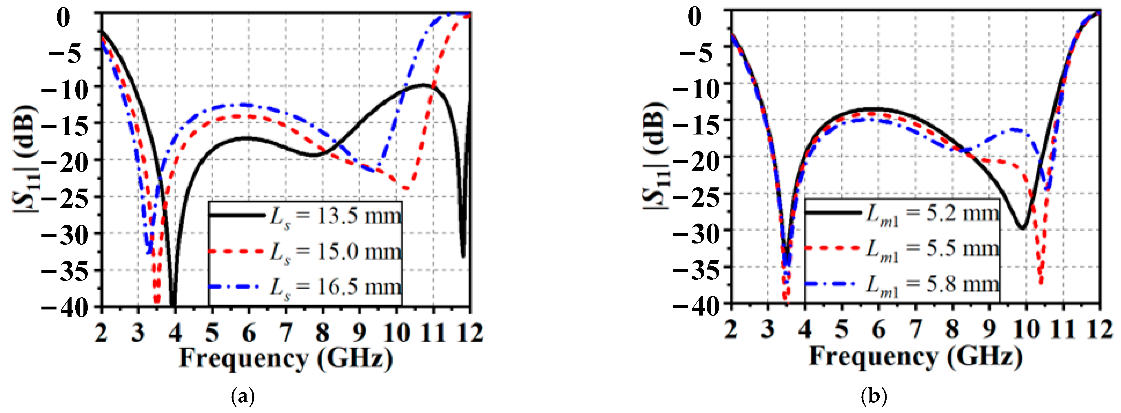
Two key parameters that affect the resonate frequencies are shown in Figure 3. It is readily seen that the length of the notch slot (Ls) determines the absorption band. All the resonances decrease to lower frequencies as Ls increases. On the other hand, the length of the z-oriented open microstrip line (Lm1) mainly affects the two higher resonances (fb2 and fb3). As Lm1 decreases, fb2 and fb3 get closer to each other.
To further illustrate the operating principle of the wideband absorption of the proposed absorber utilizing the coupled microstrip line, the current distributions on the proposed and original absorber at fa1, fa2 and fa3 are plotted in Figure 4. It can be seen that no current flows through the resistor at fa2, resulting in a reflection band. However, for the proposed absorber, the coupled current on the U-shaped microstrip line flows through the resistor at all of the three frequencies, resulting in a wide absorption band from fa1 to fa3.

2.3. Alternative Design without the Reflecting Plate

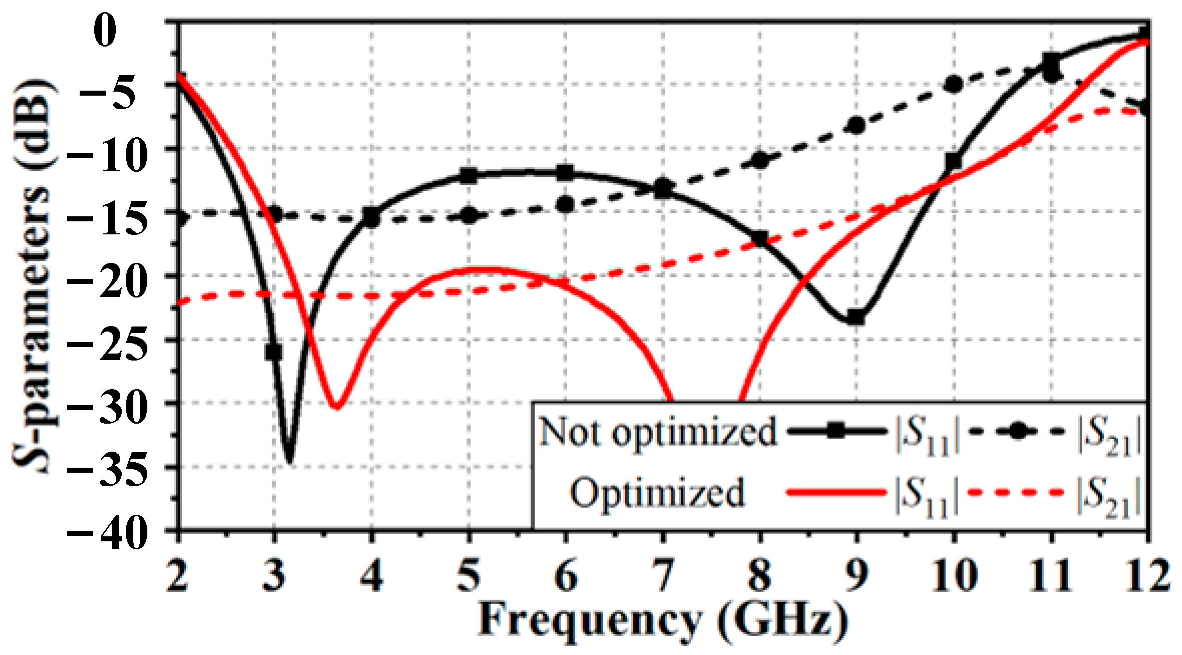
Unlike the conventional 2D absorbers, the absorption of the proposed absorber depends on the resonances of the 3D notch slot. It is therefore easy to understand that the reflecting plate is not mandatory. In other words, the absorber still works without the reflecting plate at the expense of small leakage (the transmission coefficient is not zero without the reflecting plate).
The simulated S-parameters of the proposed absorber without the reflecting plate is shown in Figure 5 (black curves). Two resonances can be observed, and |S11| is below −10 dB from 2.45 GHz to 10.10 GHz. However, |S21| gradually increases as the frequency increases. |S21| is around −15 dB below 6 GHz, but it increases to −5 dB at 10 GHz. It is fortunate that |S21| can be decreased by simply optimizing the structure (L, Lp and h). It can be seen that after optimizing, |S21| is smaller than −10 dB below 10.6 GHz. Therefore, an absorption band (|S11| ≤ −10 dB and |S21| ≤ −10 dB) is obtained from 2.6 GHz to 10.6 GHz (121.21% FBW), which is nearly the same as that of the absorber with the reflecting plate.

3. Dual-Polarized 3D absorber

3.1. Description of the Structure

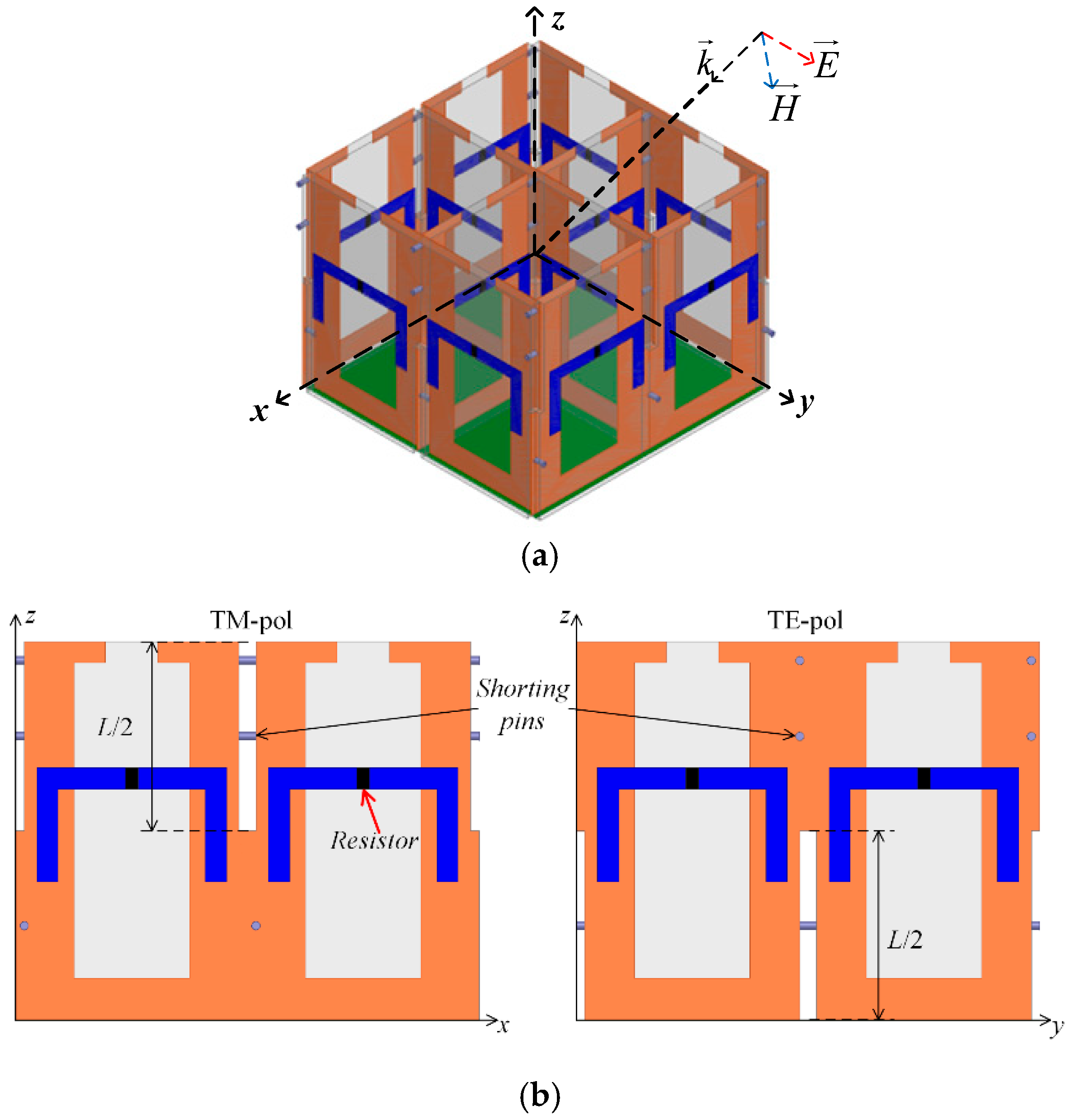
In this section, a dual-polarized 3D absorber is proposed for dual-polarized wave absorption. The notch-slot resonators with coupled U-shaped microstrip lines are arranged along the x- and y-axes, and they are responsible for TM and TE polarizations, respectively, as shown in Figure 6. Considering the fabrication, the substrates along the x- and y-axes should be cross-joined together through the securing slits cut between the two adjacent unit cells. Compared with the single-polarized design in Section 2, additional notch slots with a length of L/2 and a width of t are etched on the top and bottom sides of the unit cells for TM and TE polarizations, respectively, as shown in Figure 6b. These slots may introduce unexpected resonances that deteriorate the absorption. Therefore, some shorting pins are added inside the slots to eliminate these unexpected resonances. The shorting pins fabricated on the unit cells for TE polarization are inside the slot of the unit cells for TM polarization and vice versa. The difference is that there are two shorting pins inside the slot of the unit cells for TM polarization, and there is only one for TE polarization.

3.2. Simulation and Analysis

To illustrate the effects of the short pins, Figure 7a presents the simulated reflection coefficients of the dual-polarized 3D absorber with/without the shorting pins. It can be seen that without the shorting pins, there are reflection poles at f1 = 4.70 GHz for TM polarization and f2 = 10.04 GHz for TE polarization, respectively, which are caused by the slots between two unit cells with a length of L/2. It can be seen that f2 ≈ 2f1 because the slot for TM polarization is open at one end, while the slot for TE polarization is short at both ends. Figure 7b shows the current distributions around the slots. Typical quarter-wavelength and half-wavelength current distributions can be observed at f1 for TM polarization and at f2 for TE polarization, respectively. These resonances cause reflections at f1 and f2, which are within the absorption band. They can be simply eliminated by adding some shorting pins. The shorting pins should be loaded in the open end for TM polarization, as well as in the middle of the slots for both TM and TE polarizations. In this way, the lengths of the slots are reduced by half; therefore, the resonant frequencies are doubled and out of the absorption band. It can be seen in Figure 7a that with the shorting pins, the reflection poles are eliminated, and the absorption band from 2.64 GHz to 10.96 GHz for both TE and TM polarizations is obtained, which is similar to the one with single- polarization proposed in Section 2.
Finally, the design guidelines of the proposed 3D absorber are presented as follows:
  • The design of the open-ended notch-slot resonator. The length of the notch slot (Ls) is a quarter wavelength at the fundamental resonant frequency fa1, which is close to the starting frequency of the target absorption band (flow). Therefore, Ls can be initially calculated by Ls = c/(4 × flow). On the other hand, a larger width of the notch slot (Ws) results in a wider absorption band. However, Ws should not be close to the period of the unit cell (Lp) because the metal of the notch-slot resonator serves as the ground of the U-shaped microstrip line. Hence, the initial choice of Ws is Lp/2.
  • The design of the coupled U-shaped microstrip line. The length of the y-oriented part (Lm2) is between Ws and Lp; therefore, the initial value can be chosen as 0.75Lp. The length of the x-oriented part (Lm1) can be determined by the center frequency of the absorption band, which is roughly 2flow, so that Lm1 = c/(2 × flow) − Lm2/2.
  • A substrate with a low permittivity and high rigidity is preferred. RO4350B was therefore chosen in our design.
  • Optimize the parameters (especially the above-mentioned key parameters) to obtain a wide absorption band.

3.3. Fabrication and Measurement

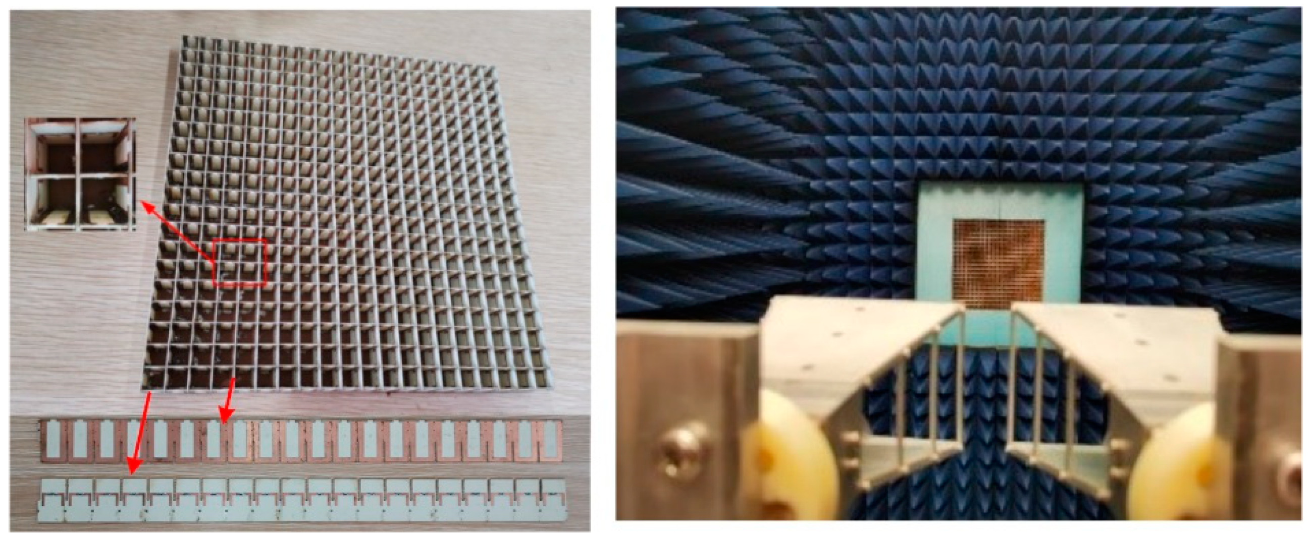
A prototype of the proposed dual-polarized 3D absorber with 20×20 unit cells was fabricated and measured using the conventional free-space measurement to verify our design, as shown in Figure 8. The measurement was carried out in an anechoic chamber. The prototype was placed 4.5m away from the two horn antennas. The measurement procedure can be referred to [19].
The measured |S11| of the proposed dual-polarized 3D absorber under the normal incidence is shown in Figure 9. The measured absorption band is from 2.74 GHz to 11.08 GHz (120.7% FBW), which agrees well with the simulated one. The small discrepancy may be due to fabrication errors.
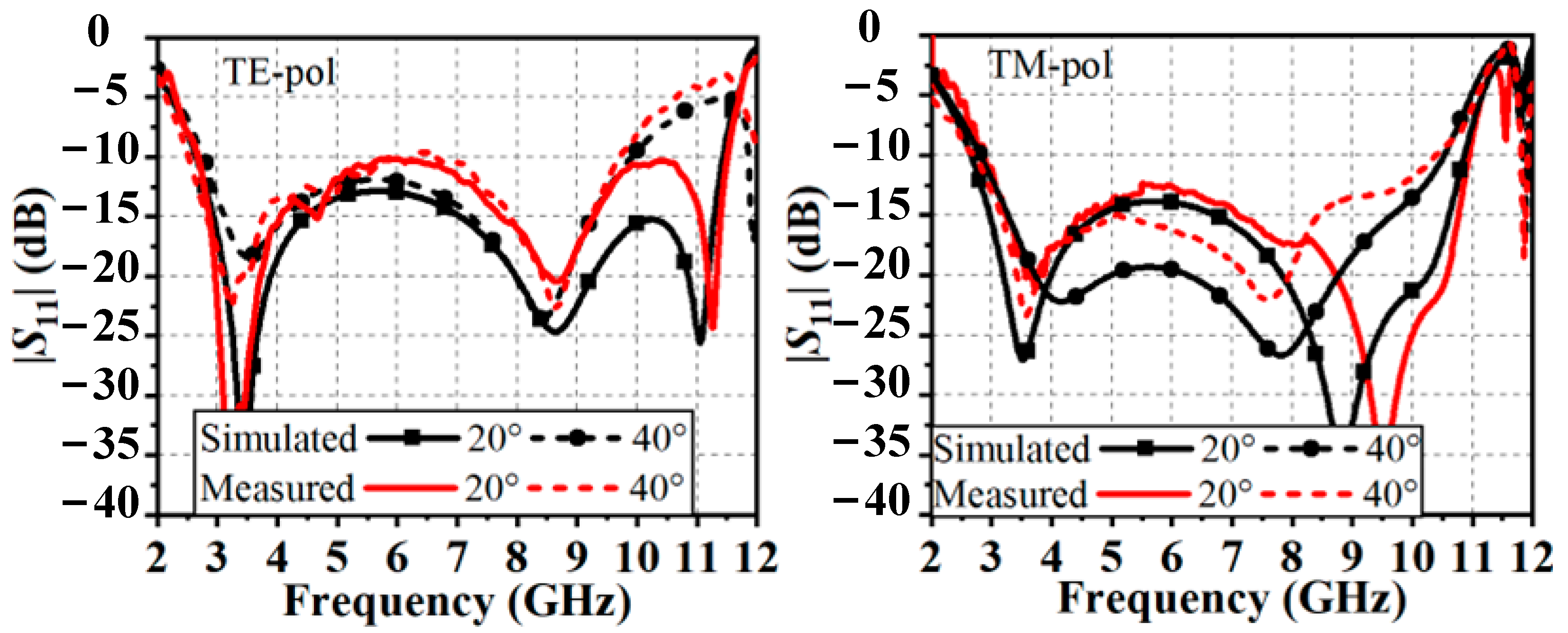
Figure 10 shows the measured and simulated |S11| of the proposed dual-polarized absorber under different (TE and TM) polarizations and incident angles (20° and 40°). The measured results are in good agreement with the simulated ones, indicating a stable absorption performance up to a 40° incident angle.
Finally, a comparison of the proposed 3D absorber with some recently reported absorbers is shown in Table 1. It can be seen that the proposed 3D absorber features the least usage of lumped components in a unit cell. It is also worth mentioning that the proposed 3D absorber can be free of a reflecting plate (see Section 2.3), which is distinct from other absorbers. The reason for this is the utilization of 3D notch-slot resonators, which operate differently from conventional absorbers.

4. Conclusions

In this paper, a broadband 3D absorber based on a notch-slot resonator with a lossy coupled microstrip line is proposed. The coupled microstrip line eliminates the reflection band of the original lossy notch-slot resonator and merges the two separating absorption bands; hence, a wide absorption band is obtained. The proposed absorber can also operate without the reflecting plate, which is also demonstrated in this paper. A dual-polarized design is also presented, and some shorting pins were added in order to eliminate the undesirable resonances introduced by the securing slits cut between two adjacent unit cells. The measured results show that the proposed dual-polarized 3D absorber exhibits an absorption band from 2.74 GHz to 11.08 GHz (120.7% FBW).

Author Contributions

Conceptualization, Y.Y.; methodology, G.X. and Q.L.; validation, G.X. and Q.L.; formal analysis, G.X. and D.G.; data curation, G.X. and Q.L.; writing—original draft preparation, D.G. and G.X.; writing—review and editing, Y.Y. and L.P.; supervision, Y.Y. and L.P. funding acquisition, Y.Y. and L.P. All authors have read and agreed to the published version of the manuscript.

Funding

This research was funded by the Natural Science Foundation of Zhejiang Province (ZJNSF) under Grants LY22F010020 and LR21F010002; and the National Natural Science Foundation of China under Grants 62171168, 61875051 and 62271439.

Data Availability Statement

Not applicable.

Conflicts of Interest

The authors declare no conflict of interest.

References

  1. Fante, R.L.; McCormack, M.T. Reflection properties of the Salisbury screen. IEEE Trans. Antennas Propag. 1988, 36, 1443–1454. [Google Scholar] [CrossRef]
  2. Chambers, B.; Tennant, A. Design of wideband Jaumann radar absorbers with optimum oblique incidence performance. Electron. Lett. 1994, 30, 1530–1532. [Google Scholar] [CrossRef]
  3. Munk, B.A.; Munk, P.; Pryor, J. On designing Jaumann and circuit analog absorbers (CA absorbers) for oblique angle of incidence. IEEE Trans. Antennas Propag. 2007, 55, 186–193. [Google Scholar] [CrossRef]
  4. Shang, Y.; Shen, Z.; Xiao, S. On the design of single-layer circuit analog absorber using double-square-loop array. IEEE Trans. Antennas Propag. 2013, 61, 6022–6029. [Google Scholar] [CrossRef]
  5. Han, Y.; Che, W. Low-profile broadband absorbers based on capacitive surfaces. IEEE Antennas Wirel. Propag. Lett. 2017, 16, 74–78. [Google Scholar] [CrossRef]
  6. Zhang, B.; Jin, C.; Shen, Z. Low-profile broadband absorber based on multimode resistor-embedded metallic strips. IEEE Trans. Microw. Theory Tech. 2020, 68, 835–843. [Google Scholar] [CrossRef]
  7. Yao, Z.; Xiao, S.; Li, Y.; Wang, B.Z. Wide-angle, ultra-wideband, polarization-independent circuit analog absorber. IEEE Trans. Antennas Propag. 2022, 70, 7276–7281. [Google Scholar] [CrossRef]
  8. Ding, F.; Cui, Y.; Ge, X.; Jin, Y.; He, S. Ultra-broadband microwave metamaterial absorber. Appl. Phys. Lett. 2011, 100, 103506. [Google Scholar] [CrossRef] [Green Version]
  9. Deng, G.; Yu, Z.; Yang, J.; Yin, Z.; Li, Y.; Chi, B. A miniaturized 3-D metamaterial absorber with wide angle stability. IEEE Microw. Wirel. Compon. Lett. 2022, 32, 1111–1114. [Google Scholar] [CrossRef]
  10. Shi, T.; Jin, L.; Han, L.; Tang, M.C.; Xu, H.X.; Qiu, C.W. Dispersion-engineered, broadband, wide-angle, polarization-independent microwave metamaterial absorber. IEEE Trans. Antennas Propag. 2021, 69, 229–238. [Google Scholar] [CrossRef]
  11. Rashid, A.K.; Shen, Z.; Aditya, S. Wideband microwave absorber based on a two-dimensional periodic array of microstrip lines. IEEE Trans. Antennas Propag. 2010, 58, 3913–3922. [Google Scholar] [CrossRef]
  12. Omar, A.A.; Shen, Z. Double-sided parallel-strip line resonator for dual-polarized 3-D frequency-selective structure and absorber. IEEE Trans. Microw. Theory Tech. 2017, 65, 3744–3752. [Google Scholar] [CrossRef]
  13. Yu, Y.; Shen, Z.; Deng, T.; Luo, G. 3-D frequency-selective rasorber with wide upper absorption band. IEEE Trans. Antennas Propag. 2017, 65, 4363–4367. [Google Scholar] [CrossRef]
  14. Luo, G.Q.; Yu, W.; Yu, Y.; Zhang, X.H.; Shen, Z. A three-dimensional design of ultra-wideband microwave absorbers. IEEE Trans. Microw. Theory Tech. 2020, 68, 4206–4215. [Google Scholar] [CrossRef]
  15. Zhang, W.; Li, B.; Zhu, L.; Lyu, Y.P.; Cheng, C.H. Stacked slotline structure-based unit cell and its application for synthesis of 3-D bandpass frequency-selective surfaces. IEEE Trans. Antennas Propag. 2020, 68, 7958–7968. [Google Scholar] [CrossRef]
  16. Zhang, Y.; Li, B.; Zhu, L.; Tang, Y.; Chang, Y.; Bo, Y. Frequency selective rasorber with low insertion loss and dual-band absorptions using planar slotline structures. IEEE Antennas Wirel. Propag. Lett. 2018, 17, 633–636. [Google Scholar] [CrossRef]
  17. Behdad, N.; Sarabandi, K. A wide-band slot antenna design employing a fictitious short circuit concept. IEEE Trans. Antennas Propag. 2005, 53, 475–482. [Google Scholar] [CrossRef] [Green Version]
  18. Ren, H.; Yu, Y.; Shen, Z. Broadband circularly-polarised antenna consisting of four notch slot radiators. Electron. Lett. 2012, 48, 1447–1449. [Google Scholar] [CrossRef]
  19. Yao, Z.; Xiao, S.; Jiang, Z.; Yan, L.; Wang, B.Z. On the design ultrawideband circuit analog absorber based on quasi-single-layer FSS. IEEE Antennas Wirel. Propag. Lett. 2020, 19, 591–595. [Google Scholar] [CrossRef]
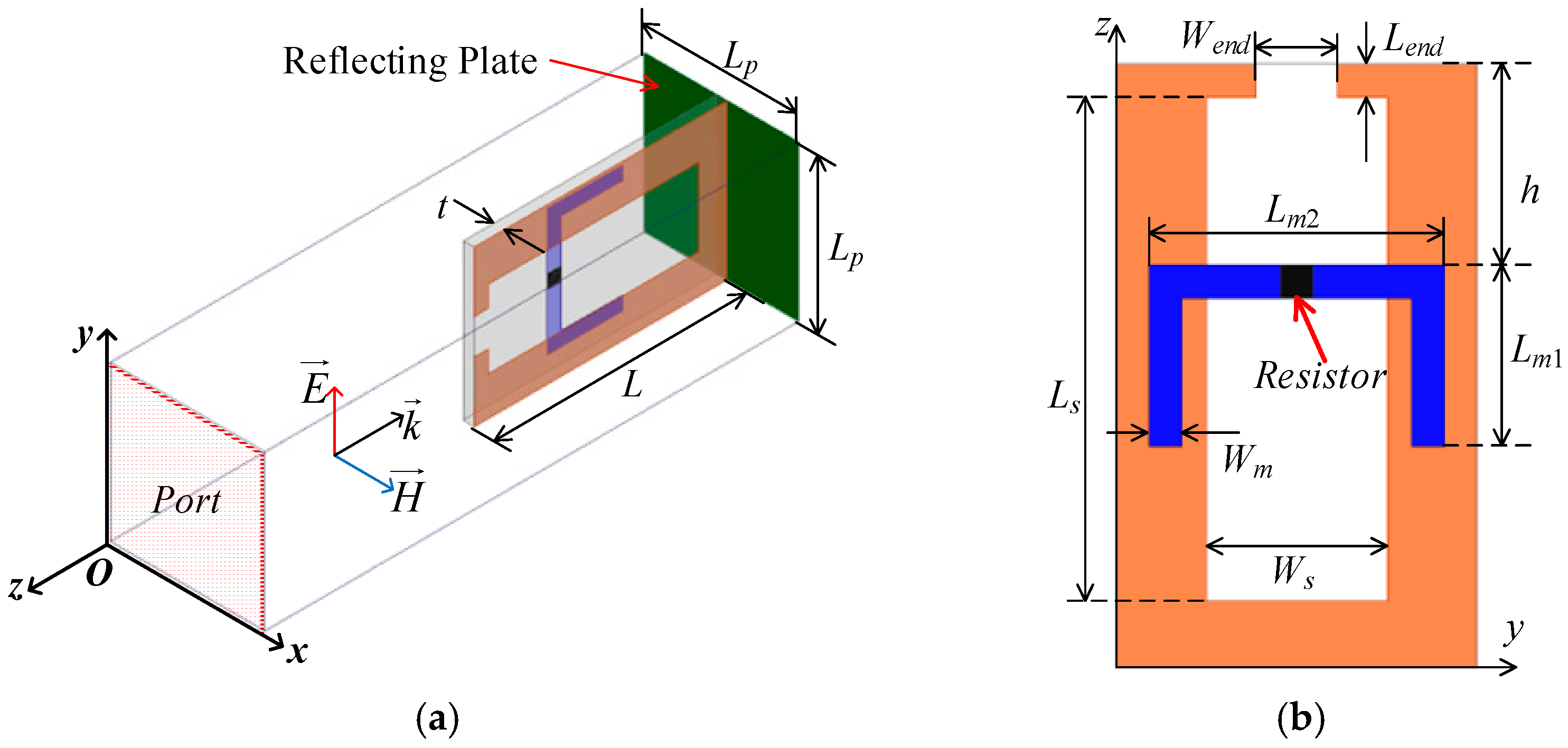
Figure 1. (a) Perspective and (b) 2D view of the proposed single-polarized 3D absorber.
Applsci 12 11082 g001
Figure 2. (a) Simulated |S11| of the proposed and the original 3D absorber; (b) simulated input impedance of the proposed and the original 3D absorber.
Applsci 12 11082 g002
Figure 3. Simulated |S11| of the proposed absorber with different structure parameters: (a) Ls and (b) Lm1.
Applsci 12 11082 g003
Figure 4. Current distribution of (a) the original lossy slotline and (b) the proposed 3D absorber.
Applsci 12 11082 g004
Figure 5. Simulated |S11| and |S21| of the proposed 3D absorber without the reflecting plate.
Applsci 12 11082 g005
Figure 6. Structure of the proposed dual-polarized absorber: (a) 3D view (2×2 unit cells); (b) 2D view of two unit cells for TM and TE polarizations.
Applsci 12 11082 g006
Figure 7. (a) Simulated |S11| of the proposed dual-polarized 3D absorber with/without the shorting pins; and (b) current distribution at the reflection frequencies.
Applsci 12 11082 g007
Figure 8. Photograph of the fabricated prototype and the measurement set-up.
Applsci 12 11082 g008
Figure 9. Simulated and measured |S11| of the proposed 3D absorber under the normal incidence.
Applsci 12 11082 g009
Figure 10. Simulated and measured |S11| of the proposed 3D absorber under the oblique incidences.
Applsci 12 11082 g010
Table 1. Comparison of the proposed 3D absorber and other absorbers.
ReferenceThickness (λL 1)FBW (%)Number of Lumped Components in a Unit Cell
[4]0.088126.88
[6]0.096159.116
[7]0.113137.18
[10]0.09159.36
[11]0.100112.03
[12]0.101148.016
This work0.164120.72
1 λL is the wavelength at the lowest frequency of the absorption band.
Publisher’s Note: MDPI stays neutral with regard to jurisdictional claims in published maps and institutional affiliations.