Article

A TSV-Structured Room Temperature p-Type TiO2 Nitric Oxide Gas Sensor

1
Institute of Microelectronics, Department of Electrical Engineering, National Cheng Kung University, Tainan 701, Taiwan
2
Taiwan Semiconductor Research Institute, Tainan 704, Taiwan
3
Department of Electronic Engineering, National Kaohsiung University of Science and Technology, Kaohsiung 807, Taiwan
*
Author to whom correspondence should be addressed.
Appl. Sci. 2022, 12(19), 9946; https://doi.org/10.3390/app12199946
Submission received: 9 September 2022 / Revised: 23 September 2022 / Accepted: 1 October 2022 / Published: 3 October 2022
(This article belongs to the Special Issue Physics and Mechanics of New Materials and Their Applications 2021)

Abstract

:
Planar MOS/MEMS gas sensors have been widely studied and applied, but the detection of exhaled gas has been little developed. The flow rate of exhaled gas affects the suspension structure of the MEMS gas sensor and the operating temperature of the gas sensor. Therefore, this study uses the Bosch process and the atomic layer deposition (ALD) process to prepare a room-temperature (RT) TSV-structured TiO2 gas sensor. The results indicated that the TiO2 sensing film is uniformed and covers the through-silicon via (TSV) structure and the TiO2 sensing film is confirmed to be a p-type MOS. In terms of gas sensing at room temperature, the response of the sensor increases with the increasing NO concentration. The sensor response is 16.5% on average, with an inaccuracy of <± 0.5% for five cycles at 4 ppm NO concentration. For gas at 10 ppm, the response of the sensor to NO is 24.4%, but the sensor produces almost no response to other gases (CO, CO2, SO2, and H2S). The RT TiO2 gas sensor with a TSV structure exhibits good stability, reversibility, and selectivity to NO gas.
Keywords:
TiO2; TSV; gas sensor

1. Introduction

Air quality is important since pollutant gases affect human health. Among them, nitrogen dioxide (NO2) gas and nitric oxide (NO) gas are two types of nitrogen oxides (NOx). The main source of these gases is as a natural product of fossil fuel combustion, thus improving the fuel’s quality has an effect on production. Moreover, it was known that combustion facilities and automobiles are the major pollutants of NOx gas. They cause airway inflammation, acid rain, and photochemical smog [1,2,3,4]. In terms of the airway inflammation, NO has been a subject of research in the biomedical field due to its pivotal role in cell signaling and is implicated in the pathophysiology of various diseases [5,6]. In a study by Kim et al., it was reported that by conducting tests on children who exhaled NO, a link to allergic inflammation was observed [7]. Taylor et al. used exhaled NO measurements to guide the management of chronic asthma [8].
Several types of gas sensors are commercially available. They are categorized as electrochemical sensors, catalytic combustion sensors or optical sensors. In recent years, metal oxide semiconductor (MOS) gas sensors have been widely studied. For instance, Pour et al. reported the performance of gas nanosensor in 1–4% of hydrogen concentration [9]. In addition, Aval et al. reported the influence of oxide film surface morphology and thickness on the properties of gas sensitive nanostructure sensor [10]. These are categorized as n-type semiconductors, such as SnO2 [11], ZnO [12], and WO3 [2], and p-type semiconductors, such as CuO [13] and Co3O4 [14]. However, due to the convenience of the circuit design and signal transmission, reducing gases are usually detected using n-type semiconductors and oxidizing gases are detected using p-type semiconductors. Titanium dioxide (TiO2) is an n-type semiconductor with a 3.0 eV energy gap and with the advantage of chemical and thermal stability at room temperature, which contributes to its suitability for gas sensing [15]. Some p-type TiO2 have been produced using a different growth technology [16,17,18].
Three-dimensional (3D) through-silicon via (TSV) technology allows heterogeneous integration, low power consumption, and reduction in the size of component. Therefore, it is widely used in integrated circuits (IC), humidity sensors [19], light-emitting diodes [20,21], field emissions [22], and photo detectors [23]. Recently, various TSV processes were widely developed, such as laser drilling [24], cryogenic etching [25], Bosch etching [26], and wet anisotropic etching [27]. Among them, the Bosch process is widely used due to its high etch rate, better profile control, and mask selectivity [26]. In addition, the Bosch process creates scallops on the sidewalls [26], which increase the sensing surface of the gas sensor. However, thin films are difficult to deposit on the surface of scallops. The atomic layer deposition (ALD) process was found to have good step coverage, especially for TSV structures [28].
This study uses a via-structured p-type TiO2 NO gas sensor that is produced by the Bosch and the ALD process. During the gas measurement, the sensor is operated at RT. A via-structured gas sensor makes the airflow considerably smoother than a MOS gas sensor with a general structure, which is more suitable for the detection of exhaled gas, especially for the detection of respiratory diseases, as shown in Figure 1. The via-structured formation, the TiO2 fabrication, and the sensor’s sensing mechanism are described and discussed.

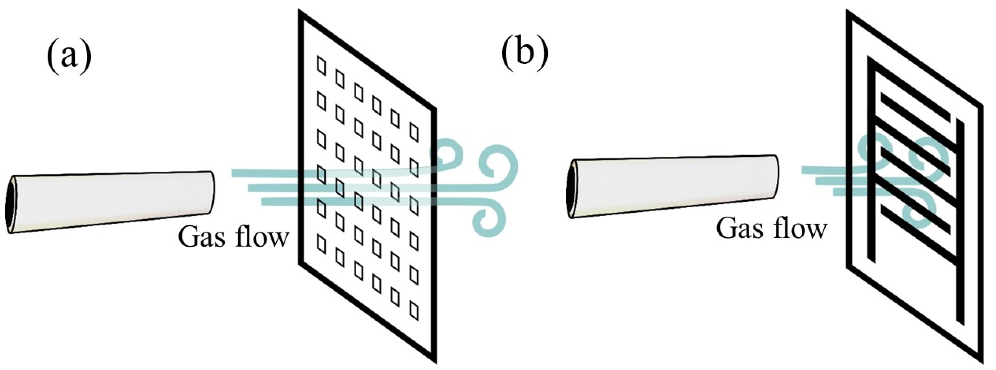
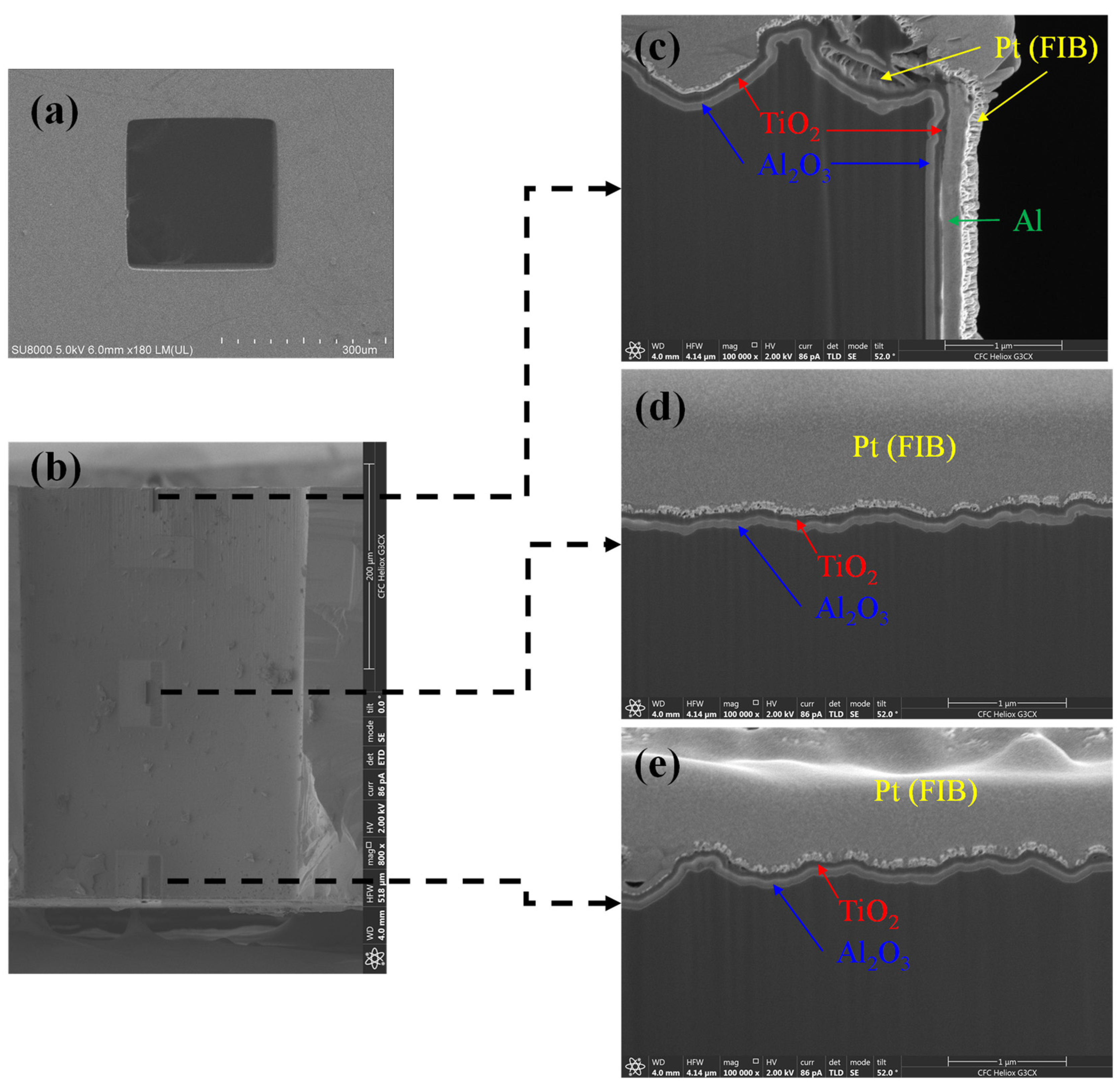
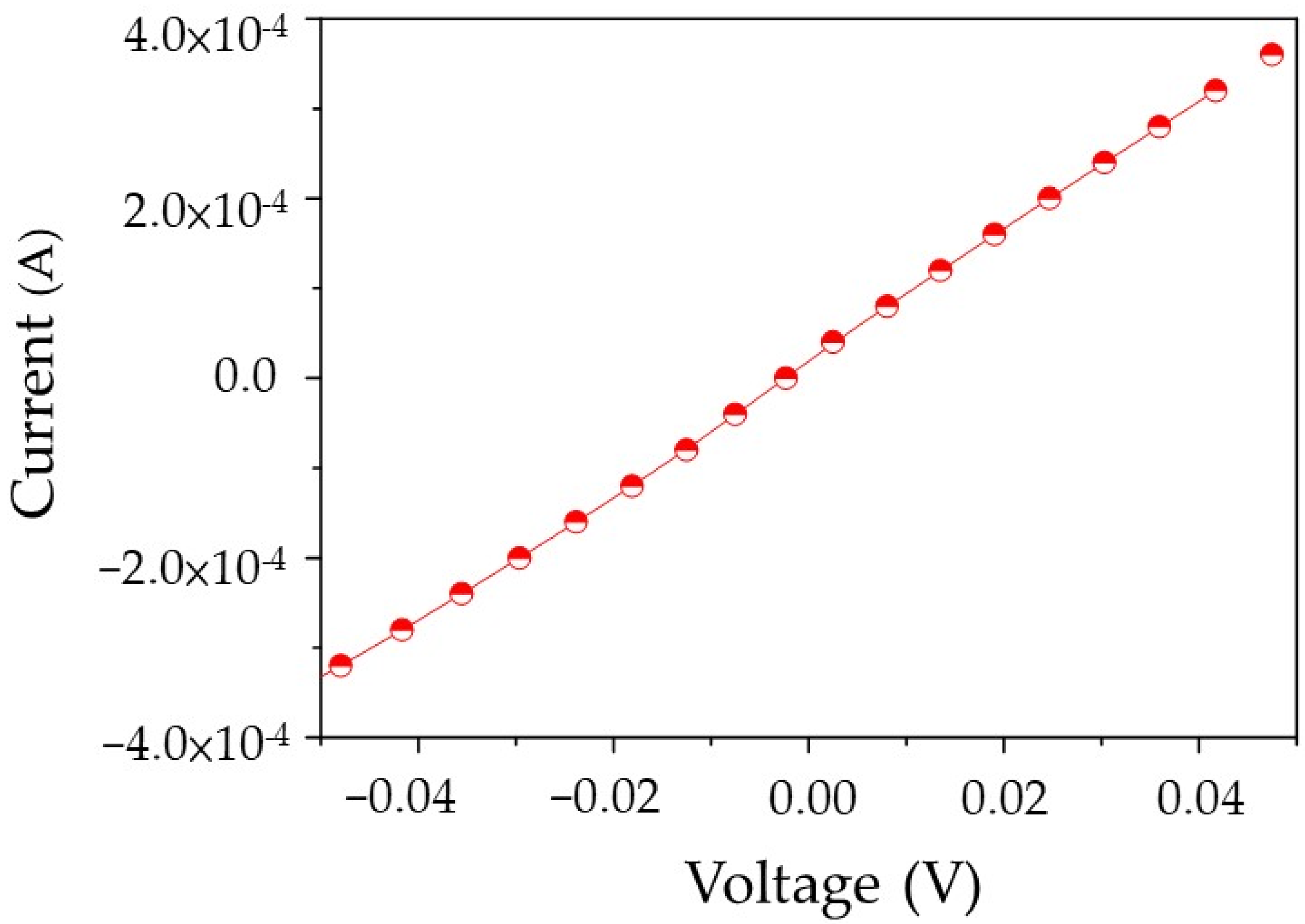
2. Materials and Methods
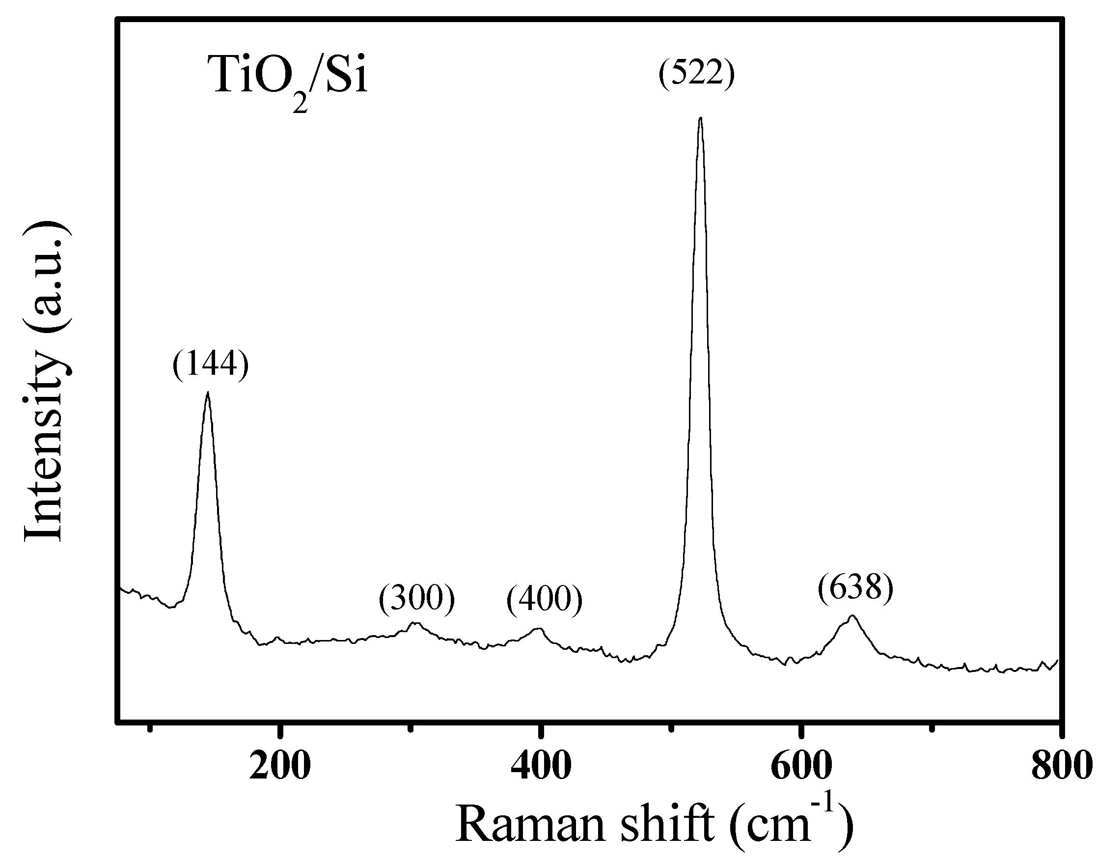
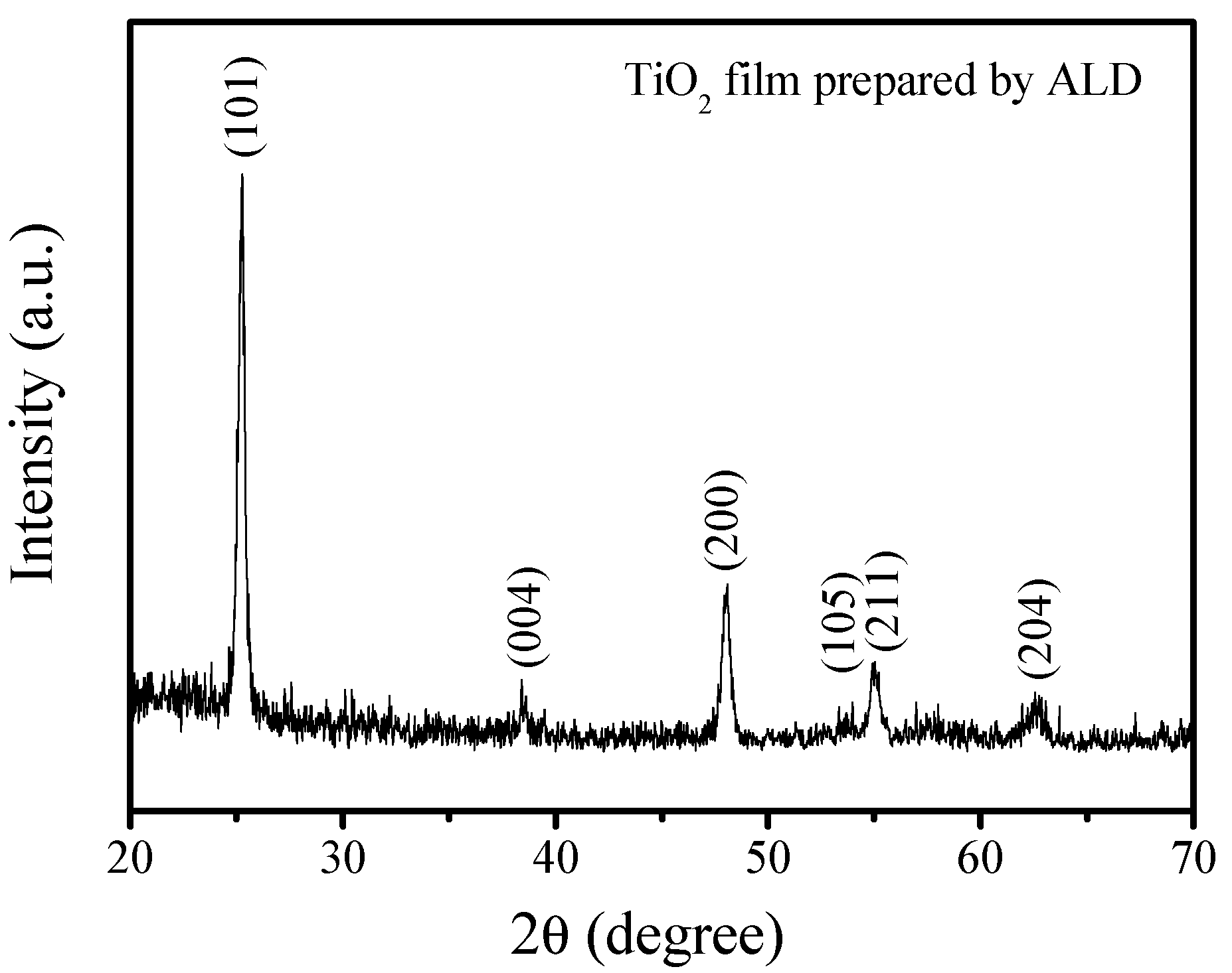
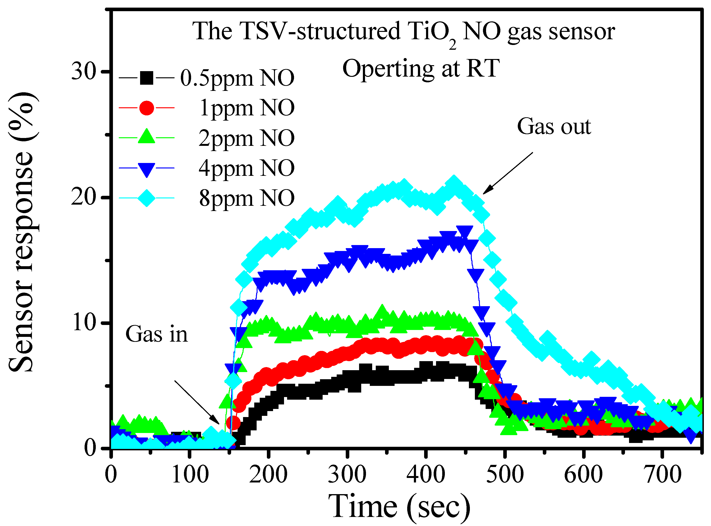
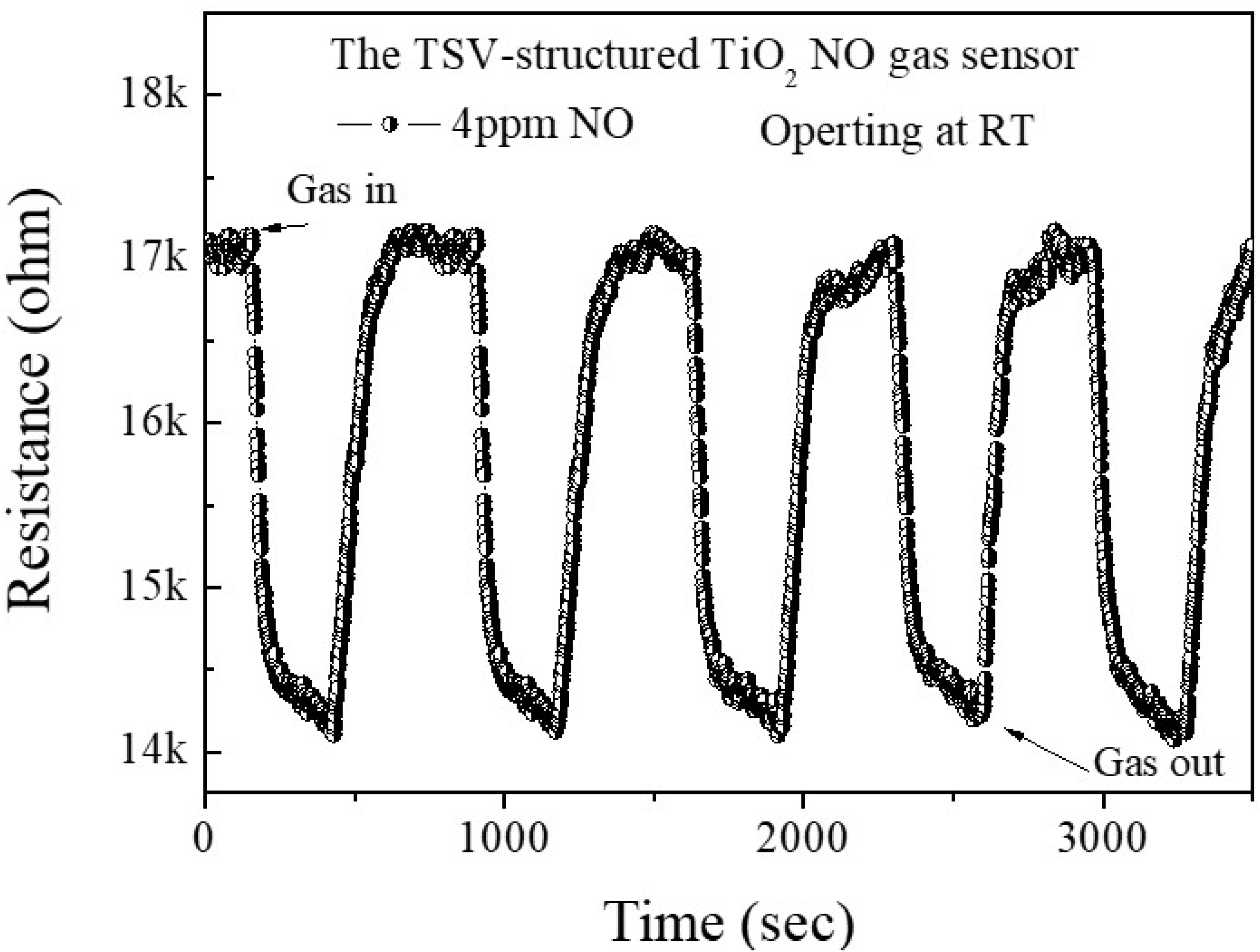
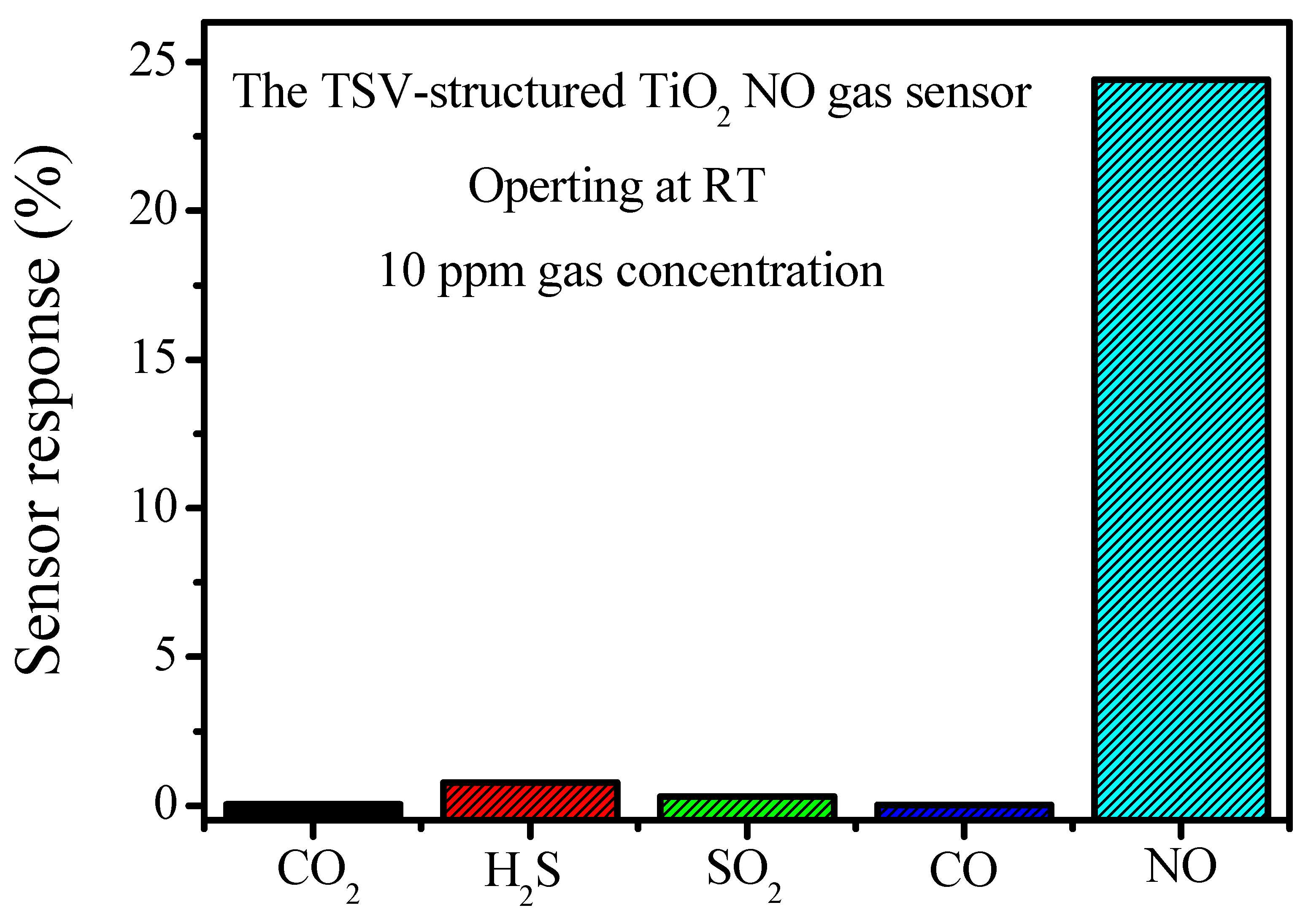
Figure 2 displays the sensor’s fabrication process diagram in this study. The fabrication process has four stages. The first stage forms the via. The via’s pattern is defined on a 6” silicon (Si) wafer using standard exposure and development processes, then the Bosch process [29] is utilized to etch Si for via’s formation, as shown in Figure 2a. The second stage produces the isolation layer. An 85 nm Al2O3 isolation layer is deposited using an ALD process to cover the surface and sidewall of the via structure, as shown in Figure 2b. The third stage produces the sensing layer. A 75 nm TiO2 is deposited on Al2O3 as a sensing layer using identical ALD equipment, as shown in Figure 2c. During the deposition of the TiO2 sensing layer, the precursors are TiCl4 and H2O vapor with an 80 sccm nitrogen (N2) carrier gas. The pressure and temperature for the process are 300 mtorr and at 300 °C, respectively. The sequence for each cycle is H2O (0.5 s), N2 (30 s), TiCl4 (0.5 s), and N2 (30 s). The TiO2 sensing layer is continuously fabricated for 1000 cycles. The final stage produces the metal electrode. A 190 nm thick aluminum layer is prepared on the double side of the substrate using radio frequency (RF) magnetron sputtering, as shown in Figure 2d.
The PlasmaPro 100 equipment was used to complete the Bosch process. The ALD was fabricated using a Picosun. The crystallinity of the TiO2 sensing layer was analyzed using an X-ray diffraction (XRD). The thickness of the Al2O3 and TiO2 and via’s structure was determined using field-emission scanning electron microscopy (FESEM, Hitachi SU8000) and a focus ion beam microscope (FIB). For gas sensor measurements, a home-made instrument system was used to measure the sensor’s response. The system includes a Keithley 2400, a personal computer, a gas injection port, and an 8.8-L volume chamber. The NO gas used for measurement is a mixture of nitrogen and nitric oxide in a ratio of 97:3. When measuring, the applied voltage of the sensor is 8 V, and a 1-L gas bag collects the gas. Then, a micro syringe is used to inject the gas with an appropriate concentration from the gas injection port into the test chamber [30].

3. Results

Figure 3a shows the top-view SEM image of the via-structured TiO2 sensor. The via is almost square, with a side length of 270 um. Figure 3b shows the cross-sectional FIB image of the via-structured TiO2 sensor. The via is 400 um deep. Figure 3c–e shows the FIB image of the top, middle, and bottom of the via structure, respectively. These figures show that the Al2O3 and TiO2 thin films are about 85 and 75 nm thick, respectively. The TiO2 and Al2O3 films which are produced using ALD are uniform and cover the surface of the Si. The Al electrode is 190 nm thick.
Figure 4 shows the micro-Raman spectrum for TiO2/Si at room temperature using a 532 nm solid laser excitation source. There is a strong and sharp peak at 522 cm−1. This is attributed to the Si substrate. In addition, there is one weaker peak at 300 cm−1, which is attributed to the SiO2 that is generated by the water vapor and the surface of the Si substrate during the fabrication of the TiO2 thin film [31]. Then, there is one minor peak at 144 cm−1 and three other significantly weaker peaks at 199, 400, and 638 cm−1. These peaks are attributed to the TiO2 thin film, which contains anatase crystals. The Raman peaks at 144, 199, and 638 cm−1 are attributed to the Raman mode position Eg mode for TiO2. These Eg peaks are attributed to the symmetric stretching vibration of O-Ti-O [21]. The peak at 400 cm−1 is attributed to the B1g mode, which is probably related to the bending vibration of O−Ti−O [32].
To confirm the structure of the TiO2 thin film, Figure 5 displays the XRD diffraction pattern of the TiO2 thin film prepared by ALD. It was found that the main diffraction plane and sub-main peak are the (101) and (200) planes, respectively. Moreover, it was found that the reflections from the (101), (004), (200), (105), (211), and (204) planes correspond to peaks at 2θ = 25.25°, 38.41°, 48.06°, 53.63°, 55.10°, and 62.68°, respectively. These features of the XRD pattern indicate the presence of an anatase phase of TiO2 (JCPDS card no. 21-1272) [33].
Hall measurement is used to confirm the type of metal oxide semiconductor material. Figure 6 shows the I-V curve for the Hall measurement, which is linear. This shows that the probes at the sample and measurement are in ohmic contact. The carrier concentration is +3.84 × 1018 cm−3. The TiO2 thin film for this study that is produced using ALD is a p-type semiconductor material, as well as the experimental conclusions that can be drawn.
Electrons have an important role in the gas sensing mechanism for a p-type MOS sensor. When the sensor is placed in air at room temperature, oxidizing gases (such as O2, nitric oxide (NO), etc.) are chemisorbed onto the surface of the MOS sensor. O2 traps an electron from the sensor’s surface to form oxygen ions (O2). The minority carriers in p-type MOS are electrons (e) and the majority carriers are holes (h+), thus when O2 captures an electron, the number of hole carriers increases since the electron-hole (e-h+) pair recombination is inhibited and the resistance of the sensor is decreased. When a reducing gas (e.g., SO2, H2S, etc.) is injected, it reacts with oxygen ions, thus the trapped electrons return to the material and there is an increase in e--h+ pair recombination and the resistance of the p-type MOS increases. With this sensing mechanism, ((Rair − Rgas)/Rair) × 100 [34] and ((Rgas − Rair)/Rair) × 100 [35], respectively define the response of the sensor to oxidizing gas and reducing gas, where Rair is the sensor’s resistance and Rgas is the sensor’s resistance in air containing an oxidizing or reducing gas. Using this definition, Figure 7 displays the sensor response of the TSV-structured TiO2 sensor. During the measurement, the NO concentration is increased from 0.5 to 8 ppm and the sensor operates at room temperature (RT). The respective sensor response for the TSV-structured TiO2 gas sensor is 6.4%, 8.2%, 10.9%, 16.7%, and 21.3% for NO concentrations of 0.5, 1, 2, 4, and 8 ppm. In other words, the response of the sensor is increased with the increasing NO concentration.
The stability and reproducibility of the TSV-structured TiO2 NO gas sensor was measured over five cycles. Each cycle involves 5 min of NO gas injection and 5 min of pumping, as shown in Figure 8. During the measurement, the NO concentration is 4 ppm and the operating temperature is RT. The sensor’s resistance rapidly decreases when NO gas is injected. The sensor’s resistance increases when the test chamber is pumped. Of note, at this time, the ambient gas is also introduced. This dynamic behavior is consistent with the sensing mechanism for a p-type MOS that is previously described. Using the same definition for sensor response, the average sensor response is 16.5%, with an inaccuracy of <±0.5%. In other words, the sensor is stable and reversible at RT. Moreover, it was found that the average response and recovery time of the TSV-structured TiO2 NO gas sensor are about 109 and 144 s. The response and recovery time are defined as the time required for a 90% change in the signal. Furthermore, this result indicated that the TSV-structured TiO2 NO gas sensor had a better response and recovery time than the previous studies [36,37,38,39,40], as shown in Table 1.
A MOS gas sensor must sense a specific gas selectively. Figure 9 shows the measurements for a TSV-structured RT TiO2 gas sensor. During this experiment, CO2, SO2, H2S, CO, and NO were injected at a flow rate of about 10 ppm. The sensor’s response to NO is 24.4%. The sensor is only very slightly responsive to gases, such as CO, H2S, SO2, and CO2. The TiO2 gas sensor with TSV structure exhibits good selectivity to NO gas. This should be attributed to the lower activation energy of TiO2 film for NO gas. Furthermore, since the sensor operates at room temperature, the TiO2 surface is difficult to adsorb ionized oxygen species. As a result, the response of the sensor is poor when reducing gases, such as CO2, CO, H2S, and SO2, are introduced [41].

4. Conclusions

This study uses the Bosch process to form a TSV structure and then uses the ALD process to fabricate a TSV-structured TiO2 gas sensor. The FIB images show that the TiO2 sensing film uniformly covers the TSV structure. The Hall measurement confirms that the TiO2 sensing film is a p-type MOS. The respective sensor response of the TSV-structured TiO2 gas sensor to NO at room temperature is 6.4%, 8.2%, 10.9%, 16.7%, and 21.3% for NO concentrations of 0.5, 1, 2, 4, and 8 ppm. In terms of the TSV-structured RT TiO2 NO gas sensor’s stability and reproducibility, the sensor response is 16.5% on average, with an inaccuracy of <±0.5%. In terms of selective gas measurement, the response of the sensor to NO is 24.4%. The sensor is only very slightly responsive to gases, such as SO2, CO, H2S, and CO2. In other words, a RT TiO2 gas sensor with a TSV structure exhibits good stability, reversibility, and selectivity to NO gas.

Author Contributions

Conceptualization, Y.-M.Y. and T.-J.H.; methodology, Y.-M.Y.; validation, Y.-M.Y., P.-H.W. and T.-J.H.; formal analysis, T.-J.H.; investigation, Y.-M.Y. and P.-H.W.; resources, S.-J.C. and T.-J.H.; data curation, P.-H.W. and T.-J.H.; writing—original draft preparation, Y.-M.Y. and T.-J.H.; writing—review and editing, T.-J.H.; visualization, T.-J.H.; supervision, T.-J.H.; project administration, T.-J.H.; funding acquisition, T.-J.H. All authors have read and agreed to the published version of the manuscript.

Funding

This research was funded by NSTC of Taiwan grant number 110-2221-E-992-047, 111-2221-E-992-029-MY3, 111-2218-E-992-001-MBK, 111-2218-E-006-011-MBK.

Institutional Review Board Statement

Not applicable.

Informed Consent Statement

Not applicable.

Data Availability Statement

Not applicable.

Acknowledgments

The authors thank the National Science and Technology Council of Taiwan for financial support and the Taiwanese Semiconductor Research Institute.

Conflicts of Interest

The authors declare no conflict of interest.

References

  1. Afzal, A.; Cioffi, N.; Sabbatini, L.; Torsi, L. NOx sensors based on semiconducting metal oxide nanostructures. Progress and perspectives. Sens. Actuator B Chem. 2012, 171, 25–42. [Google Scholar] [CrossRef]
  2. Akamatsu, T.; Itoh, T.; Izu, N.; Shin, W. NO and NO2 sensing properties of WO3 and Co3O4 based gas sensors. Sensors 2013, 13, 12467–12481. [Google Scholar] [CrossRef] [PubMed] [Green Version]
  3. Cui, L.; Han, F.; Dai, W.; Murray, E.P. Influence of microstructure on the sensing behavior of NOx exhaust gas sensors. J. Electrochem. Soc. 2014, 161, B34–B38. [Google Scholar] [CrossRef]
  4. Qin, Y.; Shen, W.; Li, X.; Hu, M. Effect of annealing on microstructure and NO2 sensing properties of tungsten oxide nanowires synthesized by solvothermal method. Sens. Actuators B Chem. 2011, 155, 646–652. [Google Scholar] [CrossRef]
  5. Tseliou, E.; Bessa, V.; Hillas, G.; Delimpoura, V.; Papadaki, G.; Roussos, C.; Papiris, S.; Bakakos, P.; Loukides, S. Exhaled nitric oxide and exhaled breath condensate pH in severe refractory asthma. CHEST 2010, 138, 107–113. [Google Scholar] [CrossRef] [PubMed]
  6. Barnes, P.J.; Liew, F.Y. Nitric oxide and asthmatic inflammation. Immunol. Today 1995, 16, 128–130. [Google Scholar] [CrossRef]
  7. Choi, B.S.; Kim, K.W.; Lee, Y.J.; Baek, J.; Park, H.B.; Kim, Y.H.; Sohn, M.H.; Kim, K.E. Exhaled Nitric Oxide is Associated with Allergic Inflammation in Children. J. Korean Med. Sci. 2011, 10, 1265–1269. [Google Scholar] [CrossRef] [Green Version]
  8. Smith, A.D.; Cowan, J.O.; Brassett, K.P.; Herbison, G.P.; Taylor, R.D. Use of Exhaled Nitric Oxide Measurements to Guide Treatment in Chronic Asthma. N. Engl. J. Med. 2005, 352, 2163–2173. [Google Scholar] [CrossRef] [PubMed] [Green Version]
  9. Pour, G.B.; Aval, L.F.; Esmaili, P. Performance of gas nanosensor in 1–4 percent hydrogen concentration. Sens. Rev. 2019, 39, 622–628. [Google Scholar] [CrossRef]
  10. Pour, G.B.; Aval, L.F. Influence of oxide film surface morphology and thickness on the properties of gas sensitive nanostructure sensor. Indian J. Pure Appl. Phys. 2019, 57, 743–749. [Google Scholar]
  11. Ji, H.; Qin, W.; Yuan, Z.; Meng, F. Qualitative and quantitative recognition method of drug-producing chemicals based on SnO2 gas sensor with dynamic measurement and PCA weak separation. Sens. Actuators B Chem. 2021, 348, 130698. [Google Scholar] [CrossRef]
  12. González-Garnica, M.; Galdámez-Martínez, A.; Malagón, F.; Ramos, C.D.; Santana, G.; Abolhassani, R.; Panda, P.K.; Kaushik, A.; Mishra, Y.K.; Karthik, T.V.K.; et al. One dimensional Au-ZnO hybrid nanostructures based CO2 detection: Growth mechanism and role of the seed layer on sensing performance. Sens. Actuators B Chem. 2021, 337, 129765. [Google Scholar] [CrossRef]
  13. Hou, J.L.; Hsueh, T.J. Temperature-Dependent n-Type and p-Type Sensing Behaviors of CuO Nanosheets/MEMS to NO2 Gas. ACS Appl. Electron. Mater. 2021, 3, 4817–4823. [Google Scholar] [CrossRef]
  14. Hsueh, T.J.; Wu, S.S. Highly sensitive Co3O4 nanoparticles/MEMS NO2 gas sensor with the adsorption of the Au nanoparticles. Sens. Actuators B Chem. 2021, 329, 129201–129209. [Google Scholar] [CrossRef]
  15. Chang, T.J.; Hsueh, T.J. A NO2 gas sensor with a TiO2 nanoparticles/ZnO/MEMS-structure that is produced using ultrasonic wave grinding technology. J. Electrochem. Soc. 2020, 167, 027521–027525. [Google Scholar] [CrossRef]
  16. Wang, S.; Pan, L.; Song, J.J.; Mi, W.; Zou, J.J.; Wang, L.; Zhang, X. Titanium-Defected Undoped Anatase TiO2 with p-Type Conductivity, Room-Temperature Ferromagnetism, and Remarkable Photocatalytic Performance. J. Am. Chem. Soc. 2015, 137, 2975–2983. [Google Scholar] [CrossRef]
  17. Fu, A.; Chen, X.; Tong, L.; Wang, D.; Liu, L.; Liu, L.; Ye, J. Remarkable Visible-Light Photocatalytic Activity Enhancement over Au/p-type TiO2 Promoted by Efficient Interfacial Charge Transfer. ACS Appl. Mater. Interfaces 2019, 11, 24154–24163. [Google Scholar] [CrossRef] [PubMed]
  18. Tang, H.; Prasad, K.; Sanjinés, R.; Lévy, F. TiO2 anatase thin films as gas sensors. Sens. Actuators B Chem. 1995, 26, 71–75. [Google Scholar] [CrossRef]
  19. Hsu, C.L.; Tsai, J.Y.; Hsueh, T.J. Ethanol gas and humidity sensors of CuO/Cu2O composite nanowires based on a Cu through-silicon via approach. Sens. Actuators B Chem. 2016, 224, 95–102. [Google Scholar] [CrossRef]
  20. Lu, C.L.; Chang, S.J.; Chen, W.S.; Hsueh, T.J. Through-Silicon via Submount for Flip-Chip LEDs. ECS J. Solid State Sci. Technol. 2017, 6, R159–R162. [Google Scholar] [CrossRef] [Green Version]
  21. Lu, C.L.; Chang, S.J.; Chen, W.S.; Hsueh, T.J. 3D RGB Light Emitting Diodes Prepared by Through Silicon Via Technology. ECS J. Solid State Sci. Technol. 2018, 7, R156–R159. [Google Scholar] [CrossRef]
  22. Hsu, C.L.; Tsai, J.-Y.; Hsueh, T.J. Novel field emission structure of CuO/Cu2O composite nanowires based on copper through silicon via technology. RSC Adv. 2015, 5, 33762–33766. [Google Scholar] [CrossRef]
  23. Lam, K.T.; Chen, Y.H.; Hsueh, T.J.; Chang, S.J. A 3-D ZnO-Nanowire Smart Photo Sensor Prepared with Through Silicon via Technology. IEEE Trans. Electron Devices 2016, 63, 3562–3566. [Google Scholar] [CrossRef]
  24. Pan, C.T.; Chen, Y.C.; Wang, S.Y.; Cheng, Y.T.; Yen, C.K.; Lin, Y.L.; Shih, W.C. TSV by 355 UV laser for 4G component packaging with micro-electroforming. Microelectron. Reliab. 2017, 78, 331–338. [Google Scholar] [CrossRef]
  25. Kamto, A.; Divan, R.; Sumant, A.V.; Burkett, S.L. Cryogenic inductively coupled plasma etching for fabrication of taperedthrough-silicon vias. J. Vac. Sci. Technol. A 2010, 28, 719–725. [Google Scholar] [CrossRef]
  26. Ranganathan, N.; Lee, D.Y.; Youhe, L.; Lo, G.Q.; Prasad, K.; Pey, K.L. Influence of Bosch Etch Process on Electrical Isolation of TSV Structures. IEEE Trans. Compon. Packag. Manuf. Technol. 2011, 1, 1497–1507. [Google Scholar] [CrossRef]
  27. Mauer, L.B.; Taddei, J.; Youssef, R.; Lu, Y.; Collins, S.; McLaughlin, K.; Allen, C. Wet Silicon Etch Process for TSV Reveal. In Proceedings of the 2014 IEEE 64th Electronic Components and Technology Conference, Orlando, FL, USA, 27–30 May 2014; pp. 878–882. [Google Scholar]
  28. Knaut, M.; Junige, M.; Neumann, V.; Wojcik, H.; Henke, T.; Hossbach, C.; Hiess, A.; Albert, M.; Bartha, J.W. Atomic layer deposition for high aspect ratio through silicon vias. Microelectron. Eng. 2013, 107, 80–83. [Google Scholar] [CrossRef]
  29. Wang, Z.; Jiang, F.; Yu, D.Q.; Zhang, W.Q. Si Etching for TSV Formation. ECS Trans. 2014, 60, 407–412. [Google Scholar] [CrossRef]
  30. Hsueh, T.J.; Lee, S.H. A La2O3 Nanoparticle SO2 Gas Sensor that Uses a ZnO Thin Film and Au Adsorption. J. Electrochem. Soc. 2021, 168, 077507–077515. [Google Scholar] [CrossRef]
  31. Das, M.; Sarkar, D. Morphological and optical properties of n-type porous silicon: Effect of etching current density. Bull. Mater. Sci. 2016, 39, 1671–1676. [Google Scholar] [CrossRef] [Green Version]
  32. Tian, F.; Zhang, Y.; Zhang, J.; Pan, C. Raman Spectroscopy: A New Approach to Measure the Percentage of Anatase TiO2 Exposed (001) Facets. J. Phys. Chem. C 2012, 116, 7515–7519. [Google Scholar] [CrossRef]
  33. Wang, M.; Zhu, Y.; Meng, D.; Wang, K.; Wang, C. A novel room temperature ethanol gas sensor based on 3D hierarchical flower-like TiO2 microstructures. Mater. Lett. 2020, 277, 128372. [Google Scholar] [CrossRef]
  34. Chethana, D.M.; Thanuja, T.C.; Mahesh, H.M.; Kiruba, M.S.; Jose, A.S.; Barshilia, H.C.; Manjanna, J. Synthesis, structural, magnetic and NO2 gas sensing property of CuO nanoparticles. Ceram. Int. 2021, 47, 10381–10387. [Google Scholar] [CrossRef]
  35. Li, D.; Tang, Y.; Ao, D.; Xiang, X.; Wang, S.; Zu, X. Ultra-highly sensitive and selective H2S gas sensor based on CuO with sub-ppb detection limit. Int. J. Hydrogen Energy 2019, 44, 3985–3992. [Google Scholar] [CrossRef]
  36. Lin, C.Y.; Chen, J.G.; Feng, W.Y.; Lin, C.W.; Huang, J.W.J.; Tunney, J.; Ho, K.C. Using a TiO2/ZnO double-layer film for improving the sensing performance of ZnO based NO gas sensor. Sens. Actuators B Chem. 2011, 157, 361–367. [Google Scholar] [CrossRef]
  37. Kuchi, C.; Naresh, B.; Reddy, P.S. In Situ TiO2-rGO Nanocomposite for Low Concentration NO Gas Sensor. ECS J. Solid State Sci. Technol. 2021, 10, 037008. [Google Scholar] [CrossRef]
  38. Murali, G.; Reddeppa, M.; Reddy, C.S.; Park, S.; Chandrakalavathi, T.; Kim, M.D.; In, I. Enhancing the Charge Carrier Separation and Transport via Nitrogen-Doped Graphene Quantum Dot-TiO2 Nanoplate Hybrid Structure for an Efficient NO Gas Sensor. ACS Appl. Mater. Interfaces 2020, 12, 13428–13436. [Google Scholar] [CrossRef]
  39. Khasim, S.; Pasha, A.; Hatem-Al-Aoh; Badi, N.; Imran, M.; Al-Ghamdi, S.A. Development of high-performance flexible and stretchable sensor based on secondary doped PEDOT-PSS:TiO2 nanocomposite for room-temperature detection of nitric oxide. J. Mater. Sci. Mater. Electron. 2021, 32, 7491–7508. [Google Scholar] [CrossRef]
  40. Hong, L.Y.; Lin, H.N. NO gas sensing at room temperature using single titanium oxide nanodot sensors created by atomic force microscopy nanolithography. Beilstein J. Nanotechnol. 2016, 7, 1044–1051. [Google Scholar] [CrossRef] [Green Version]
  41. Luo, P.; Xie, M.; Luo, J.; Kan, H.; Wei, Q. Nitric oxide sensors using nanospiral ZnO thin film deposited by GLAD for application to exhaled human breath. RSC Adv. 2020, 10, 14877–14884. [Google Scholar] [CrossRef]
Figure 1. (a) With and (b) without a TSV-structured gas sensor.
Applsci 12 09946 g001
Figure 2. The sensor fabrication process diagram for (a) etching Si, (b) depositing Al2O3, (c) depositing TiO2, and (d) depositing Al, respectively.
Applsci 12 09946 g002
Figure 3. (a) The top-view SEM image and (b) the cross-sectional FIB image of the via-structured TiO2 sensor (ce) show an enlarged image of the top, middle, and bottom of the via-structured sensor, respectively.
Applsci 12 09946 g003
Figure 4. The micro-Raman spectrum for TiO2/Si at room temperature.
Applsci 12 09946 g004
Figure 5. The XRD diffraction pattern of the TiO2 thin film prepared by ALD.
Applsci 12 09946 g005
Figure 6. The I-V curve for the Hall measurement.
Applsci 12 09946 g006
Figure 7. The sensor response for various concentrations.
Applsci 12 09946 g007
Figure 8. Resistance of a TSV-structured TiO2 gas sensor that is exposed to 4 ppm NO and at RT.
Applsci 12 09946 g008
Figure 9. Gas measurements for a TSV-structured TiO2 gas sensor.
Applsci 12 09946 g009
Table 1. Comparison with the previously studied TiO2 nitric oxide gas sensor.
MaterialsStructureConcentration
(ppm)
Optimum Operation
Temperature (°C)
Response
Time (s.)
Recovery Time (s.)Reference
TiO2NP/ZnO filmPlanar10360492336[36]
TiO2-rGO NanocompositePlanar2.75RT440881[37]
TiO2@NGQDsPlanar100RT235285[38]
PEDOT–PSS:DEG-TiO2Planar1RT41633[39]
TiO2 nanodotPlanar10RT91184[40]
TiO2 FilmTSV4RT109144This work
Publisher’s Note: MDPI stays neutral with regard to jurisdictional claims in published maps and institutional affiliations.

