Article

Dynamic Single-Electron Transistor Modeling for High-Frequency Capacitance Characterization

1
Graduate School of Science and Technology, Shizuoka University, Hamamatsu 432-8011, Japan
2
Graduate School of Integrated Science and Technology, Shizuoka University, Hamamatsu 432-8011, Japan
3
Research Institute of Electronics, Shizuoka University, Hamamatsu 432-8011, Japan
*
Author to whom correspondence should be addressed.
Appl. Sci. 2022, 12(16), 8139; https://doi.org/10.3390/app12168139
Submission received: 5 July 2022 / Revised: 10 August 2022 / Accepted: 12 August 2022 / Published: 14 August 2022
(This article belongs to the Section Quantum Science and Technology)

Abstract

:

Featured Application

High-frequency amplification, oscillation, detection, qubits readout by gate-based sensing, etc., based on a single-electron transistor.

Abstract

Based on the time-dependent master equation and taking the dynamic gate current into account, a new single-electron transistor (SET) model is proposed, which can represent intrinsic terminal capacitances and transcapacitances. By using this model, bias, frequency and temperature dependences of these capacitances are evaluated. Since the model is implemented in the SPICE circuit simulator, it can be used to analyze the high-frequency behavior of circuits, including SETs and is applied to the characterization of a SET-based inverting amplifier this time.

1. Introduction

Thanks to the advances in nanofabrication technology, it is possible to make single-electron transistors (SETs) small enough to realize room-temperature operation [1,2,3]. As a result, the values of source, drain and gate capacitances can be in the order of attofarad, which leads to subpicosecond intrinsic time constant even though the tunnel junction resistance is lower bounded by the resistance quantum, h/e2 about 25.8 kΩ. Such a possibility of high-speed or high-frequency operation of SETs has been discussed before simply based on this small intrinsic time constant [4,5], but now that the fabrication technology has advanced, it is worthwhile to analyze the high-frequency dynamic behavior of the SET in more detail.
For this purpose, an understanding of the capacitance components inside the SET is crucial. For example, the Miller effect caused by the feedback capacitance largely affects the frequency response of amplifiers [6]. Recently, charge detection for qubit readout is attempted by observing the gate input capacitance [7,8,9,10], which also requires SET models with capacitance analysis capability.
Historically, high-speed and high-frequency performance of SET-based circuits have been studied with models based on steady-state master equation [11,12,13,14,15,16,17], under the assumption that the external load capacitance is much larger than the internal one, but the intrinsic high-frequency response of SETs cannot be assessed by the steady-state models. Even with such a model, it is still possible to derive the capacitance components such as terminal capacitances and transcapacitances inside the SET [13], but the frequency dependence of capacitances cannot be evaluated.
Black-box models [18] and macro models [19] have similar features as long as they just provide an output current instantaneously as a function of terminal voltages.
Monte Carlo (MC) method [20,21,22] can simulate the dynamic or transient behavior of the intrinsic SET. Since the charges in the gate and source/drain tunnel capacitors are explicitly calculated, terminal capacitances and transcapacitances can also be derived from the simulation result. Actually, reference [23] discussed the input capacitance of SETs in conjunction with the electrometer sensitivity. However, MC method is usually not compatible with the standard circuit simulator such as SPICE and has difficulties in analyzing frequency-dependent behavior of SET itself or circuits including SETs and other circuit elements.
SET models based on time-dependent master equations that are capable of analyzing the dynamic behavior have been developed by many researchers [11,24,25]. Since the source/drain current can be directly expressed, implementation of the models to SPICE circuit simulator [26,27] is also straightforward. Once the model is implemented to SPICE circuit simulator, it is possible to analyze the performance of SET circuits including FETs and other circuit elements. Moreover, the MC analysis capability of SPICE allows us to study the variability issue that has become serious in nanometer-scale devices including SETs [28]. However, to the best of our knowledge, there has been no model that can properly describe the terminal capacitances and transcapacitances.
Considering the above-mentioned background, we have proposed a SET model based on the time-dependent master equation, taking the gate current into account. Our model can not only analyze the high-frequency dynamic behavior of SETs, but also can represent terminal capacitances and transcapacitances. Since this model is implemented in the SPICE circuit simulator, it can be used to evaluate the high-frequency characteristics of various SET-based circuits such as amplifier, oscillator, detector, etc.

2. Method of Modeling
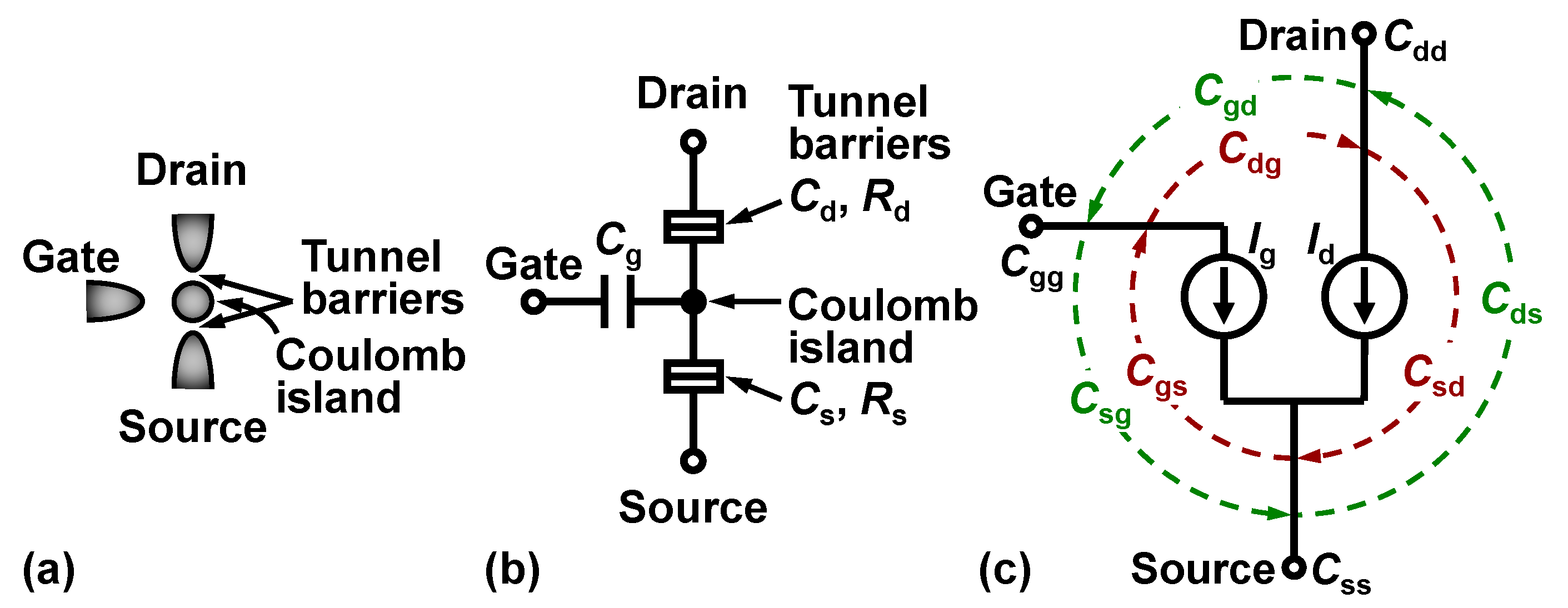
2.1. Proposed Model

The pictorial and symbolic schematics of the SETs are shown in Figure 1a,b, respectively. In the proposed model of Figure 1c, the gate current Ig and the drain current Id is calculated based on the time-dependent master equation [29]. The Ig represents the contribution of the gate terminal (input) capacitance Cgg and gate-related transcapacitances Cgd and Cgs. The contribution of other capacitances is also included in Id and Is = −(Id + Ig). Although three-terminal configuration is considered at this time for simplicity, it is also possible to extend the model to four-terminal configuration [13] with the second gate (backgate), which is useful in some circuit applications [4,11] and the analysis of the background noise effect [30] that has a large impact on the SET-based circuit integrity.
When the master equation is solved, it is assumed that number of electrons (n) in the Coulomb island can be in four states, i.e., n = −1, 0, 1 or 2. The Id is given by
Id = ePn {Γd(n − 1, n) − Γd(n + 1, n)}
Here, Pn represents the probability that the number of electrons in the island is n whereas Γd (n − 1, n) and Γd (n + 1, n) are the tunneling rates of electrons from n to n − 1 and n to n + 1 at the drain junction, respectively.
To calculate the Ig, potential of the Coulomb island Visl needs to be determined first by
V isl = C g V g + C s V s + C d V d + Q isl C
Here, Cg, Cs, and Cd are the gate, source and drain capacitances, respectively, and C = Cg + Cs + Cd. Average charge Qisl in the Coulomb island is given by
Q isl = e n P n
By substituting (3) in (2), Visl can be rewritten as
V isl = C g V g + C s V s + C d V d e n P n C
Here, Vg, Vs and Vd are gate, source and drain voltages, respectively. The Ig flowing from the gate terminal to the Coulomb island via gate capacitor can be expressed as the change in the charge Qg in gate capacitor with respect to time.
I g = d Q g d t = d d t ( V g V isl ) C g = d d t { V g ( C g V g + C d V d + C s V s e n P n C ) } C g = d d t { C g C Σ ( V g C Σ C g V g C d V d C s V s + e n P n ) }
The SPICE circuit simulator [27] is used as a solver for the simultaneous differential equation [31] of the master equation to obtain the Pn and Γd in (1) and (5).
In the following sections, the simulation results will be shown based on the parameters summarized in Table 1. These parameters are set rather arbitrarily to realize the cutoff frequency of 1 GHz where experimental verification is relatively easy and are also viable considering that the subattofarad capacitances have already been realized [1,2,3], and the tunneling resistance could be varied in a wide range by changing the insulator thickness. We also try to generalize the results by normalization, i.e., when the operation condition is described, temperature T, gate-source voltage Vgs, and drain-source voltage Vds are normalized as KBT/(e2/2C), CgVgs/e and CVds/e, respectively, and enclosed in square brackets […] if these are put down with raw values. The normalized Vgs ranges from 0 to 1 electron in the simulation since only n’s from −1 to 2 are considered in solving the master equation. Two cases of small and moderate normalized Vds of 0.01 and 0.5 are considered. The normalized temperature is set to 0.05 in most of the simulations in order not to thermally disturb the Coulomb blockade condition.

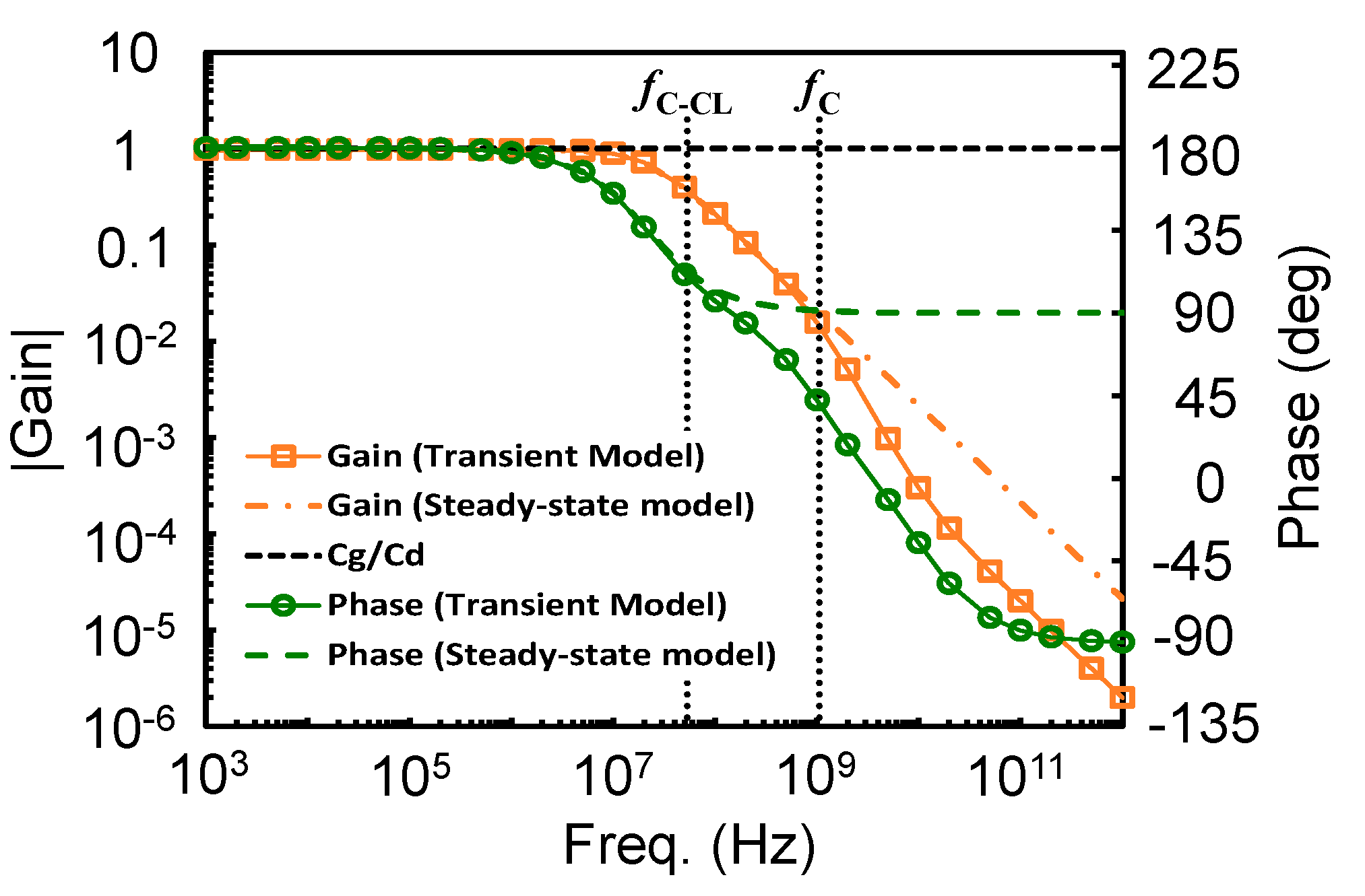
2.2. Accuracy of the Model

Since n can assume only four states, accuracy gets deteriorated if the temperature or the drain voltage becomes high. The deviation of the drain current from that of the reference MC simulator SIMON [22] is evaluated. It is found that the deviation is less than 0.5% for the normalized temperature up to 0.5 and the normalized Vds up to 2.1 with various Vgs’s around 0.5 e/Cg (data not shown).

2.3. Extraction of Capacitance Components

As shown in Figure 1, a three-terminal SET has in total 9 terminal capacitances and transcapacitances. Since the Ig current source is newly added to the proposed model, the gate input capacitance Cgg, the drain-to-gate feedback capacitance Cgd, and source-to-gate capacitance Cgs can be extracted from the simulation.
The Cgg is evaluated by the circuit shown in Figure 2a where small sinusoidal fluctuation with amplitude ∆Vgs (= e/Cg/1000) is added to the gate bias voltage Vgs, and then the amplitude ∆Ig of the gate current fluctuation is measured by the simulation. The Cgg is calculated by
C gg = Δ I g ω Δ V gs
As shown in Figure 2b, the Cgd is measured by adding small sinusoidal fluctuation with amplitude ∆Vds (= e/C/1000) to the drain bias voltage Vds, and the amplitude ∆Ig of the gate current fluctuation is observed. Similarly, the Cgd is obtained by
C gd = Δ I g ω Δ V ds
Considering that the sum of Cgd and Cgs is equal to Cgg based on charge conservation of the Cgs is given by
C gs = C gg C gd

3. Simulation Results

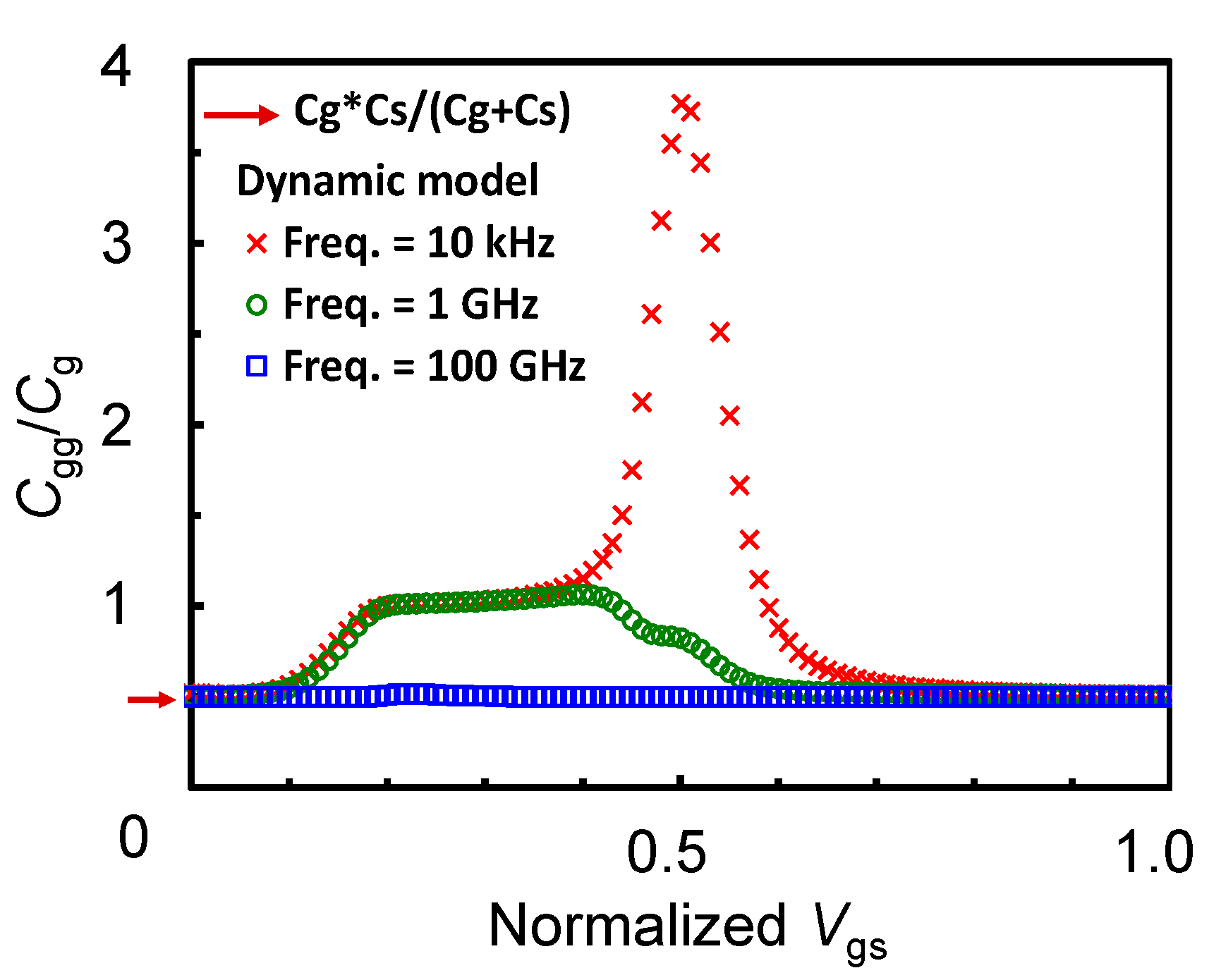
3.1. Gate Bias Dependence of Capacitances

Figure 3a–c represent the Cgg, Cgd, and Cgs, respectively, as a function of gate voltage Vgs for a low drain voltage of e/C/100 at three different frequencies. The solid line shows the result of the steady-state model [13], which coincides well with the data points (square) of the proposed model at a low frequency (10 kHz).
The Cgg shows a sharp peak at Vgs = 0.5 e/Cg, where Coulomb blockade is lifted. The peak Cgd and Cgs are almost equal to each other, and are a half of the peak Cgg, indicating that the gate is equally coupled to the drain and source at this low drain voltage.
At the cutoff frequency (1 GHz), the peak height is largely reduced, and levels off at 100 GHz due to the disappearance of the transistor action of the SET, i.e., the charge state of the Coulomb island cannot follow the rapid change of the signal. The baseline values of the Cgg, Cgd, and Cgs are Cg*(Cd + Cs)/C, Cg*Cd/C and Cg*Cs/C, respectively, which can be understood by considering the SET as a passive capacitance circuit consisting of Cg, Cd and Cs.
Figure 4a–c represent the Cgg, Cgd, and Cgs, respectively, as a function of gate voltage Vgs for a high drain voltage of e/C/2 at three different frequencies. The proposed model at a low frequency (square) and the steady-state model (solid line) [13] give the same result even at this large drain voltage.
The Cgg shows lower and wider plateau compared to the case with the low drain voltage (Figure 3a) reflecting the gentler change in the island charge with respect to Vgs, and wider Vgs area where the Coulomb blockade is lifted. In view of the behavior of the Cgd and Cgs, it is found that the gate is strongly coupled to the source at low Vgs’s, and to the drain at high Vgs’s due to the large asymmetry in applied voltages to the source and the drain.
When the frequency is increased to the cutoff frequency (1 GHz), the capacitances come close to the baselines, then level off at 100 GHz due to the loss of the transistor action. The baseline values of the capacitances are the same as those for the low drain voltage (Figure 3) and can be also explained based on the passive capacitance circuit.

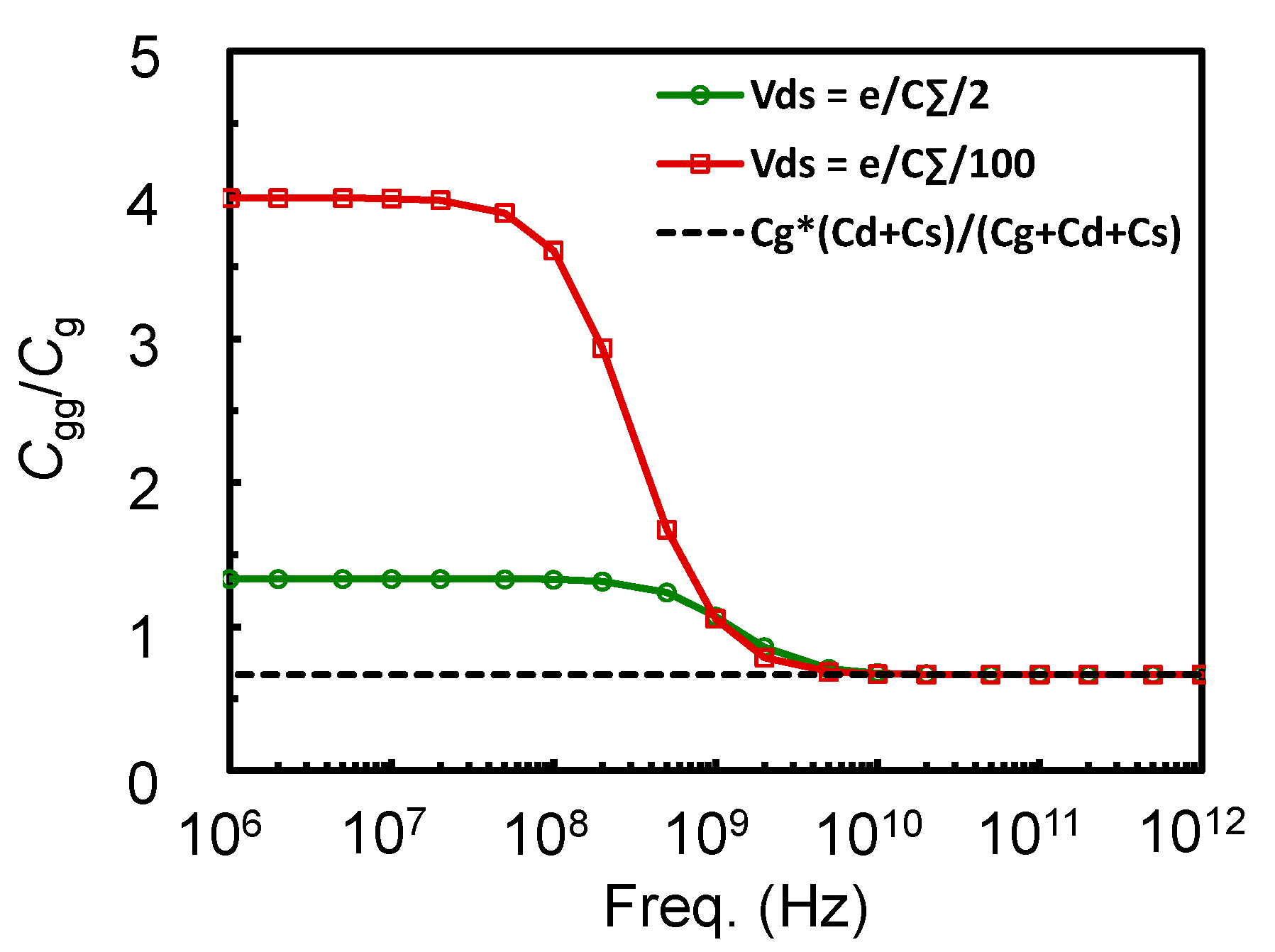
3.2. Frequency Dependence of Capacitances

Figure 5 shows the gate input capacitance Cgg as a function of frequency at low and high drain voltages of e/C/100 and e/C/2, respectively. It can be seen that the Cgg starts to decrease at a frequency about an order of magnitude lower than the cutoff frequency (1 GHz) and approaches the dashed line at higher frequencies, which can be explained again as the approach to the condition of passive capacitance circuit consisting of Cg, Cd and Cs. From such an analysis, we can quantitatively understand the frequency-dependent behaviors of the capacitances inside the SET.

3.3. Temperature Dependence of Capacitances

Figure 6 shows the gate input capacitance Cgg as a function of temperature at low and high drain voltages of e/C/100 and e/C/2, respectively. The simulation is performed up to the temperature of 15.5 K [0.5] because the proposed model is accurate up to this temperature, as was previously discussed.
For a small Vds, Cgg increases as the temperature decreases almost inversely proportional to the temperature as predicted by the quantum capacitance Cq (dashed line) [7]. This is due to the steeper change of the island charge with respect to the Vgs at lower temperatures. For a large Vds, the change of the island charge is gentle due to the wider transition region between n = 0 and 1, and thus the Cgg is small and insensitive to the temperature.
At higher temperatures, the Cgg assumes the common and nearly constant value as the Coulomb blockade is lifted, and the proposed model can describe the behavior up to the normalized temperature of 0.5 in contrast to the simplified equation of Cq.

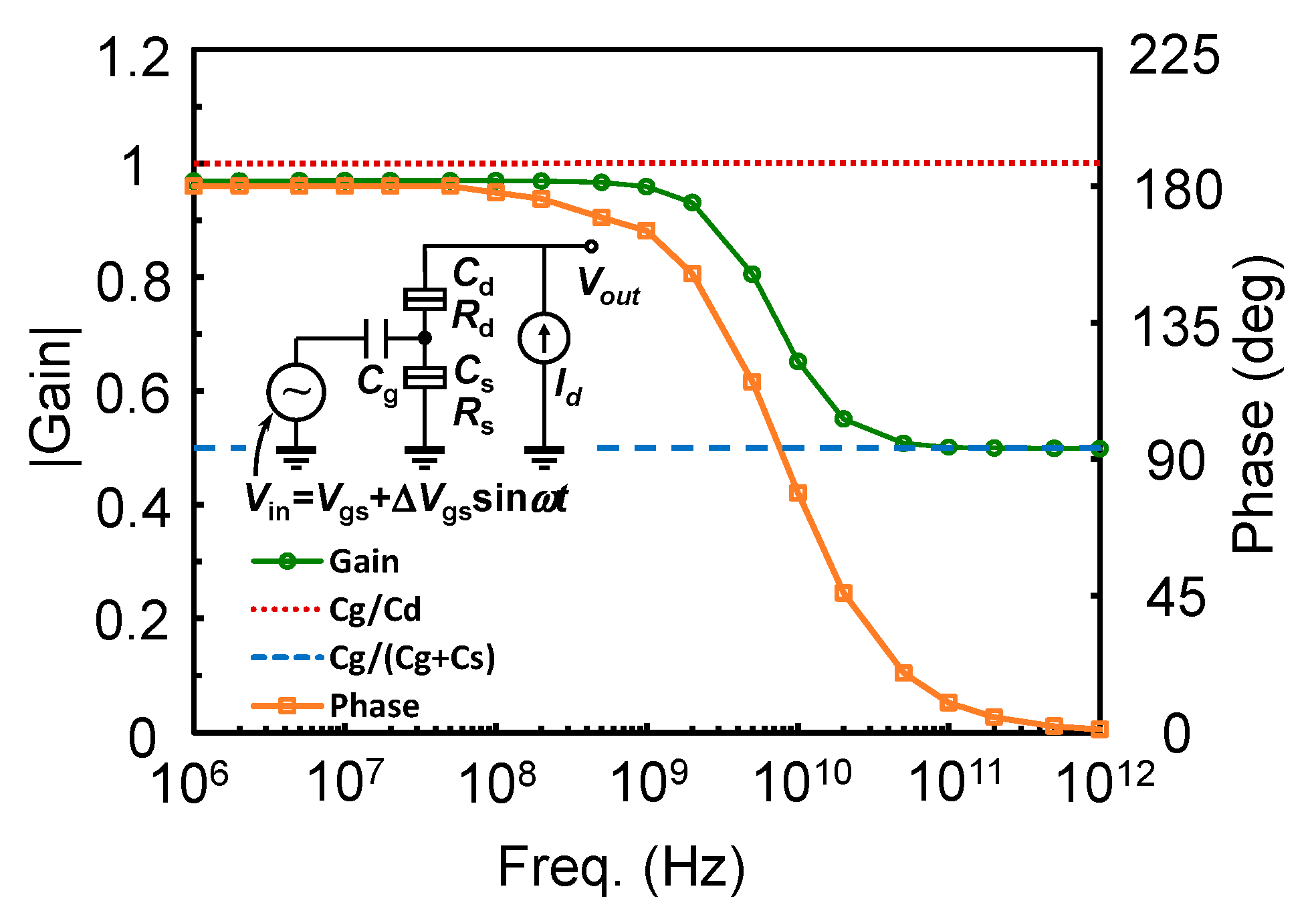
3.4. Characteristics of the SET-Based Amplifier

Figure 7a shows the circuit diagram of the SET-based inverting amplifier with a constant-current load, and Figure 7b describes the operation point in the Coulomb diamond (CD) plot. The operation point is set at the center of the descending side in the input-output (Vds-Vgs) characteristics for the Id = ±26.7 pA [=(Vds/4 Rt)/10 with Vds = e/C/2].
To evaluate the frequency response of the amplifier, small sinusoidal fluctuation with amplitude ∆Vgs (=e/Cg/1000) is added to the gate bias Vgs, and the fluctuation in Vout is observed by the simulation.
Figure 8 depicts the frequency response of the SET-based amplifier. At low frequencies, the voltage gain close to the slope of the descending side of the CD (=Cg/Cd) is obtained, and the phase is inverted. At high frequencies, the transistor action is lifted, the gain becomes that of passive capacitive divider consisting of the Cg and Cs, and the output is in phase with the input. Interestingly, the gain and phase start to change at higher frequency compared to the case in Figure 5 probably due to the high-impedance condition at the output terminal.
The input capacitance Cgg is also simulated as a function of the gate voltage Vgs at three different frequencies and shown in Figure 9.
As can be seen in the figure at the low frequency (10 kHz), the Cgg shows a high peak at Vgs = 0.5 e/Cg due to the small Vds and resultant abrupt change in the island charge. At the cutoff frequency (1 GHz), the peak height is reduced largely, and at the high frequency (100 GHz), the Cgg levels off to the baseline value that corresponds to the series connection of Cg and Cs as shown in the expression in the legend. Such behavior again verifies that the SET behaves like a passive circuit of capacitors at high frequencies.
Another interesting finding in Figure 9 is that the Miller effect [6] is not conspicuous in the SET-based amplifier as the Cgg at the operation point (Vgs = 0.33 e/Cg) is almost the same as that in Figure 4a because the feedback capacitance Cgd is negligibly small as shown in Figure 4b, suggesting that it is only necessary to take care of the parasitic capacitance when we discuss the Miller effect in the SET-based amplifier.
We have focused on the intrinsic SET characteristics so far. In reality, lead lines connected to the terminals are always accompanied by parasitic components such as capacitance, inductance, resistance, etc. As an example of a real circuit, an inverting amplifier with a load capacitance CL is analyzed (Figure 10). Actually, each terminal of SET should be connected to a constant-voltage source or a capacitor sufficiently larger than CΣ so that the SET can be regarded as an independent circuit element [13], and this time the CL is set to 30 aF (=10 CΣ). As a consequence, the cutoff frequency fC-CL of 53.1 MHz (= 1 4 π R C L ) consisting of SET output resistance and CL dominates the low-frequency part of the frequency response.
Figure 11 compares the frequency responses of SET-based amplifier with a load capacitor, simulated by the proposed transient model and the steady-state model [13]. From both curves we can see that at low frequencies voltage gain is equal to the slope of the descending side of CD, and the phase is inverted. The gain starts to decrease at around fC-CL, and continues to decrease in proportional to 1/f, but further drop is observed by the transient model at around fC where transistor action is lifted. Such a drop cannot be described by the steady-state model because the model itself is frequency-independent. The phase starts to decrease at around fC-CL and becomes saturated at 90 deg in case of the steady-state model, but it continues to decrease in the case of the transient model and finally gets saturated at −90 deg, reflecting the transition from inverting to non-inverting operations at high frequencies above the fC as observed in Figure 8, which also cannot be expressed by the steady-state model. These results clearly demonstrate the importance of the proposed transient model in accurately describing the high-frequency behavior of the real circuits.
Note that the relatively low fC-CL and fC could be increased by three orders of magnitude at the highest by decreasing the tunneling resistance to the level of the resistance quantum [32]. There is also room for decreasing the capacitance parameters by size reduction to increase the cutoff frequencies.

4. Conclusions

A model for SETs was proposed based on the time-dependent master equation and taking dynamic gate current into account, and it was realized by using the SPICE circuit simulator as a solver for simultaneous differential equations. Based on this model, intrinsic terminal capacitances and transcapacitances in the SET were discussed as a function of gate voltage, frequency, and temperature. It was concluded that, at low frequencies, the capacitances depended on the biasing but, at high frequencies, the transistor action of the SET was lifted, and it acted as a passive capacitance circuit. Such a transition from the low-frequency to high-frequency characteristics of the SET could be described quantitatively by the proposed model. Also, the model could analyze the behavior of the SET covering a wide range of temperature, in which the Cgg for small Vds was inversely proportional to the temperature on the low-temperature side, and the Cgg assumed the constant value insensitive to the temperature or Vds on the high-temperature side.
In addition, the frequency response of the SET-based amplifier was investigated. The transformation from inverting amplifier at low frequencies to the capacitive divider at high frequencies was successfully described. It was also found that the Miller effect is not conspicuous in the SET-based amplifier due to the negligible feedback capacitance at the operation point.
From these results, we can expect that the proposed model can be widely used to analyze the circuits, including SETs for high-frequency amplification, oscillation, detection, qubits readout by gate-based sensing, and so on.

Author Contributions

Conceptualization, A.S. and H.I.; Data curation, A.S.; Formal analysis, A.S. and H.I.; Methodology, A.S. and T.N.; Visualization, A.S. and H.I.; Writing original draft, A.S.; Software, T.N.; Investigation, H.S. and H.I.; Supervision, H.S. and H.I.; Resources, H.I.; Validation, H.I.; Writing—review and editing, H.I. All authors have read and agreed to the published version of the manuscript.

Funding

This research was funded by the Cooperative Research Project of the Research Center for Biomedical Engineering with RIE, Shizuoka University, and the Cooperative Research Project Program of RIEC, Tohoku University.

Institutional Review Board Statement

Not applicable.

Informed Consent Statement

Not applicable.

Data Availability Statement

The data that support the findings of this study are available from the corresponding author (H.I.) upon reasonable request.

Acknowledgments

Authors are grateful to Yuta Naito and Koki Shimizu of Shizuoka University for fruitful discussions.

Conflicts of Interest

The authors declare no conflict of interest.

References

  1. Kano, S.; Azuma, Y.; Kanehara, M.; Teranishi, T.; Majima, Y. Room-Temperature Coulomb Blockade from Chemically Synthesized Au Nanoparticles Stabilized by Acid–Base Interaction. Appl. Phys. Exp. 2010, 3, 105003. [Google Scholar] [CrossRef]
  2. Suzuki, R.; Nozue, M.; Saraya, T.; Hiramoto, T. Experimental Observation of Quantum Confinement Effect in <110> and <100> Silicon Nanowire Field-Effect Transistors and Single-Electron/Hole Transistors Operating at Room Temperature. Jpn. J. Appl. Phys. 2013, 52, 104001. [Google Scholar] [CrossRef]
  3. Nakajima, A. Application of Single-Electron Transistor to Biomolecule and Ion Sensors. Appl. Sci. 2016, 6, 94. [Google Scholar] [CrossRef]
  4. Tucker, J.R. Complementary digital logic based on the “Coulomb blockade”. J. Appl. Phys. 1992, 72, 4399–4413. [Google Scholar] [CrossRef]
  5. Mooij, J.E. Single Electrons: Status and Prospects. In Proceedings of the 1993 International Conference on Solid State Devices and Materials, Chiba, Japan, 29 August–1 September 1993; pp. 339–340. [Google Scholar] [CrossRef]
  6. Razavi, B. Design of Analog CMOS Integrated Circuits; McGraw-Hill: New York, NY, USA, 2001; pp. 166–169. [Google Scholar]
  7. Colless, J.I.; Mahoney, A.C.; Hornibrook, J.M.; Doherty, A.C.; Lu, H.; Gossard, A.C.; Reilly, D.J. Dispersive Readout of a Few-Electron Double Quantum Dot with Fast rf Gate Sensors. Phys. Rev. Lett. 2013, 110, 046805. [Google Scholar] [CrossRef] [PubMed]
  8. Gonzalez-Zalba, M.F.; Barraud, S.; Ferguson, A.J.; Betz, A.C. Probing the limits of gate-based charge sensing. Nat. Commun. 2015, 6, 6084. [Google Scholar] [CrossRef]
  9. Ahmed, I.; Haigh, J.A.; Schaal, S.; Barraud, S.; Zhu, Y.; Lee, C.-M.; Amado, M.; Robinson, J.W.A.; Rossi, A.; Morton, J.J.L.; et al. Radio-Frequency Capacitive Gate-Based Sensing. Phys. Rev. Appl. 2018, 10, 014018. [Google Scholar] [CrossRef]
  10. Schaal, S.; Rossi, A.; Ciriano-Tejel, V.N.; Yang, T.-Y.; Barraud, S.; Morton, J.J.L.; Gonzalez-Zalba, M.F. A CMOS dynamic random access architecture for radio-frequency readout of quantum devices. Nat. Electron. 2019, 2, 236–242. [Google Scholar] [CrossRef]
  11. Fujishima, M.; Amakawa, S.; Hoh, K. Circuit Simulators Aiming at Single-Electron Integration. Jpn. J. Appl. Phys. 1998, 37, 1478–1482. [Google Scholar] [CrossRef]
  12. Uchida, K.; Matsuzawa, K.; Koga, J.; Ohba, R.; Takagi, S.-I.; Toriumi, A. Analytical Single-Electron Transistor (SET) Model for Design and Analysis of Realistic SET Circuits. Jpn. J. Appl. Phys. 2000, 39, 2321–2324. [Google Scholar] [CrossRef]
  13. Inokawa, H.; Takahashi, Y. A compact analytical model for asymmetric single-electron tunneling transistors. IEEE Trans. Electron Devices 2003, 50, 455–461, Erratum in IEEE Trans. Electron Devices 2003, 50, 862–862. . [Google Scholar] [CrossRef]
  14. Mahapatra, S.; Vaish, V.; Wasshuber, C.; Banerjee, K.; Ionescu, A. Analytical modeling of single electron transistor for hybrid CMOS-SET analog IC design. IEEE Trans. Electron Devices 2004, 51, 1772–1782. [Google Scholar] [CrossRef]
  15. Miyaji, K.; Saitoh, M.; Hiramoto, T. Compact analytical model for room-temperature-operating silicon single-electron transistors with discrete quantum energy levels. IEEE Trans. Nanotechnol. 2006, 5, 167–173. [Google Scholar] [CrossRef]
  16. Pruvost, B.; Mizuta, H.; Oda, S. Voltage-limitation-free analytical single-electron transistor model incorporating the effects of spin-degenerate discrete energy states. J. Appl. Phys. 2008, 103, 054508. [Google Scholar] [CrossRef]
  17. Klupfel, F.J. A Compact Model Based on Bardeen’s Transfer Hamiltonian Formalism for Silicon Single Electron Transistors. IEEE Access 2019, 7, 84053–84065. [Google Scholar] [CrossRef]
  18. dos Santos Pês, B.; Oroski, E.; Guimarães, J.G.; Bonfim, M.J. A Hammerstein–Wiener Model for Single-Electron Transistors. IEEE Trans. Electron Devices 2018, 66, 1092–1099. [Google Scholar] [CrossRef]
  19. Yu, Y.S.; Lee, H.S.; Hwang, S.W. MacroModeling of single electron transistors for efficient circuit simulation. IEEE Trans. Electron Devices 1999, 46, 1667–1671. [Google Scholar]
  20. Korotkov, N.; Chen, R.H.; Likharev, K. Possible Performance of Capacitively Coupled Single-Electron Transistors in Digital Circuits. J. Appl. Phys. 1995, 78, 2520–2530. [Google Scholar] [CrossRef]
  21. Chen, R.H.; Korotkov, A.N.; Likharev, K.K. Single-electron transistor logic. Appl. Phys. Lett. 1996, 68, 1954–1956. [Google Scholar] [CrossRef]
  22. Wasshuber, C.; Kosina, H.; Selberherr, S. SIMON-A simulator for single-electron tunnel devices and circuits. IEEE Trans. Comput. Des. Integr. Circuits Syst. 1997, 16, 937–944. [Google Scholar] [CrossRef]
  23. Zimmerman, N.M.; Keller, M.W. Dynamic input capacitance of single-electron transistors and the effect on charge-sensitive electrometers. J. Appl. Phys. 2000, 87, 8570–8574. [Google Scholar] [CrossRef]
  24. Fonseca, L.R.C.; Korotkov, A.N.; Likharev, K.K.; Odintsov, A.A. A numerical study of the dynamics and statistics of single electron systems. J. Appl. Phys. 1995, 78, 3238–3251. [Google Scholar] [CrossRef]
  25. Kirihara, M.; Nakazato, K.; Wagner, M. Hybrid Circuit Simulator Including a Model for Single Electron Tunneling Devices. Jpn. J. Appl. Phys. 1999, 38, 2028–2032. [Google Scholar] [CrossRef]
  26. Nagel, L.W. SPICE2: A Computer Program to Simulate Semiconductor Circuits. Ph.D. Dissertation, University of California, Berkeley, CA, USA, 9 May 1975. Available online: http://www2.eecs.berkeley.edu/Pubs/TechRpts/1975/ERL-m-520.pdf (accessed on 16 December 2021).
  27. LTspice IV Version 4.231. Analog Devices, Inc. 2016. Available online: https://www.analog.com/en/design-center/design-tools-and-calculators/ltspice-simulator.html (accessed on 8 April 2022).
  28. Amat, E.; Bausells, J.; Parez-Murano, F. Exploring the Influence of Variability on Single-Electron Transistos into SET-Based Circuits. IEEE Trans. Electron Devices 2017, 64, 5172–5180. [Google Scholar] [CrossRef]
  29. Ingold, G.L.; Nazarov, Y.V. Charge Tunneling Rates in Ultrasmall Junctions. In NATO ASI Series B, Single Charge Tunneling; Grabert, H., Devoret, M.H., Eds.; Springer: Boston, MA, USA, 1992; Volume 294, pp. 77–80. [Google Scholar]
  30. Stewart, M.; Zimmerman, N. Stability of Single Electron Devices: Charge Offset Drift. Appl. Sci. 2016, 6, 187. [Google Scholar] [CrossRef]
  31. Yamamura, K.; Kuroki, W.; Okuma, H.; Inoue, Y. Path Following Circuit--SPICE-Oriented Numerical Methods Where Formulas are Described by Circuits. IEICE Trans. Fundam. Electron. Commun. Comput. Sci. 2005, E88-A, 825–831. [Google Scholar] [CrossRef]
  32. Du, S.; Yoshida, K.; Zhang, Y.; Hamada, I.; Hirakawa, K. Terahertz dynamics of electron–vibron coupling in single molecules with tunable electrostatic potential. Nat. Photon. 2018, 12, 608–612. [Google Scholar] [CrossRef]
Figure 1. (a) SET pictorial schematic, (b) symbolic schematic, and (c) model schematic with capacitance components inside the SET.
Applsci 12 08139 g001
Figure 2. Circuit diagrams for the measurement of (a) Cgg and (b) Cgd.
Applsci 12 08139 g002
Figure 3. (a) SET input capacitance Cgg (b) drain-to-gate capacitance Cgd and (c) source-to-gate capacitance Cgs as a function of gate voltage Vgs for a low drain voltage Vds = 0.534 mV [0.01] at T = 15.5 K [0.05].
Applsci 12 08139 g003
Figure 4. (a) SET input capacitance Cgg (b) drain-to-gate capacitance Cgd and (c) source-to-gate capacitance Cgs as a function of gate voltage Vgs for a high drain voltage Vds = 26.7 mV [0.5] at T = 15.5 K [0.05].
Applsci 12 08139 g004
Figure 5. SET input capacitance Cgg as a function of frequency at drain voltages Vds = 0.534 mV [0.01] and 26.7 mV [0.5], gate voltages Vgs = 80.1 mV [0.5] and 93.5 mV [0.6] and T = 15.5 K [0.05].
Applsci 12 08139 g005
Figure 6. SET input capacitance Cgg as a function of temperature at drain voltages Vds = 0.534 mV [0.01] and 26.7 mV [0.5], and gate voltages Vgs = 80.1 mV [0.5] and 93.5 mV [0.6], respectively.
Applsci 12 08139 g006
Figure 7. (a) A circuit diagram of the SET-based inverting amplifier with constant-current load, and (b) Coulomb diamond (CD) plot with Vds-Vgs curves for Id = ±26.7 pA at T = 15.5 K [0.05]. The operation point of the amplifier is set at the center of the descending side.
Applsci 12 08139 g007
Figure 8. Frequency response of the SET inverting amplifier operating at a drain current Id = 26.4 pA, gate voltage Vgs = 53.4 mV [0.33] (center of the descending side of the CD) and T = 15.5 K [0.05].
Applsci 12 08139 g008
Figure 9. SET input capacitance Cgg as a function of the gate voltage Vgs for a drain current Id = 26.7 pA at T = 15.5 K [0.05].
Applsci 12 08139 g009
Figure 10. A circuit diagram of the SET-based inverting amplifier with constant-current load and load capacitance CL.
Applsci 12 08139 g010
Figure 11. The frequency response of the SET inverting amplifier with a load capacitor CL = 30 aF (10 CΣ) operating at a drain current Id = 26.4 pA, gate voltage Vgs = 53.4 mV [0.33] (center of the descending side of the CD) and T = 15.5 K [0.05].
Applsci 12 08139 g011
Table 1. The simulation parameters.
Gate, drain and source capacitances
CgCd = Cs
1 aF
Tunneling resistances
RdRs = Rt
25 MΩ
Cutoff frequency
fc = 1 / ( 2 π R Σ C Σ )
1 GHz
Gate—source voltage
Vgs
0~162 mV [0~1]
Drain—source voltage
Vds
0.534 mV [0.01], 26.7 mV [0.5]
Temperature
T
15.5 K [0.05]
except for Figure 6.
Square brackets […] indicate normalized values.
Publisher’s Note: MDPI stays neutral with regard to jurisdictional claims in published maps and institutional affiliations.

