Article

Surface Morphology, Roughness, and Structural Characteristics of Al1−xMgxSb (x = 0 and 0.1) Thin Films Deposited by Chemical Bath Deposition Technique

1
Department of Physics, The University of Lahore, Lahore 54000, Pakistan
2
School of Materials Science and Engineering, Zhejiang University, Hangzhou 310027, China
3
Centre of Excellence in Solid State Physics, University of the Punjab, Lahore 54590, Pakistan
4
Department of Physics, Riphah International University, Lahore Campus, Lahore 54000, Pakistan
5
Hangzhou Global Scientific and Technological Innovation Center, Zhejiang University, Hangzhou 310027, China
6
Department of Nanoengineering, Kyonggi University, Suwon 16227, Korea
*
Authors to whom correspondence should be addressed.
Appl. Sci. 2022, 12(15), 7412; https://doi.org/10.3390/app12157412
Submission received: 13 June 2022 / Revised: 13 July 2022 / Accepted: 21 July 2022 / Published: 23 July 2022
(This article belongs to the Special Issue Feature Papers in Surface Sciences and Technology Section)

Abstract

:
Aluminum antimonide (AlSb), a semiconductor compound, finds its applications in optoelectronics because of its tunable bandgap and promising properties achieved by tailoring suitable dopants. To explore the effects of doping, thin films of pure AlSb and 10% magnesium (Mg)-doped aluminum antimonide (MgAlSb) were synthesized through compound solution deposition on a glass substrate using a low-cost chemical bath deposition (CBD) technique at varying bath temperatures with deposition time intervals ranging from 60 to 180 min. Optical microscopy was used to evaluate the surface roughness and morphology of the synthesized films, revealing the surface roughness and thin film uniformity at different deposition times. The structural characteristics of AlSb and Mg-doped AlSb thin films were further examined using the X-ray diffraction technique, which validated the formation of AlSb and Mg-doped AlSb thin films. This research enables large-scale low-temperature deposition for a variety of conceivable applications in the coatings, materials penetration, energy, and photonic sectors due to the novel properties of this material.

1. Introduction

Aluminum antimonide is an efficient semiconductor compound in the III-V group with a 1.62 eV indirect bandgap having high electron mobility, which makes it an ideal material to be used as an anode material for a range of applications, including transistors, photovoltaic devices, thermal radiation detectors, and the PN junction diodes [1,2,3]. In addition, both aluminum and antimony are nontoxic and abundantly found on Earth with their efficient properties, such as high absorption and high charge carrier mobility. The AlSb semiconductor was theoretically demonstrated and regarded as an extremely efficient material for photoelectric conversion with a recorded efficiency of 27% and has the potential to be employed in photovoltaic applications [3]. Sputtering, electrodeposition [2,3], molecular beam epitaxy [4], vapor deposition [5], pulsed laser deposition [6], and the hot wall epitaxial growth method [7] are all traditional techniques for the synthesis of AlSb compounds. However, experiments have been reported to synthesize AlSb thin films using the pulsed laser deposition (PLD) method [6], which demonstrated the influence of moisture on resultant AlSb thin films by the interaction of Al and Sb ions [8]. Both n-type and p-type dopants have already been reported for AlSb films in previous studies, where Shaw [9] and Wieber [10] investigated the diffusion of zinc (Zn) and copper (Cu) in AlSb semiconductors. Likewise, Lilli et al. synthesized Cu-doped AlSb films on a quartz substrate using the co-sputtering technique, where the AlSb was doped with Cu, which served as an interstitial atom to raise the lattice constant, wherein Cu-doped AlSb exhibited significantly different results than undoped AlSb after the annealing procedures, which proved the fact that the position of the doping atom is the most significant factor in investigating material characteristics. These results demonstrate the high impact of the annealing procedure on thin film deposition to obtain the desired material properties [11]. Moreover, Shawon et al. reported a doping method for Mg as a dopant in AlSb films using controlled melting and vacuum hot-pressing in which they replaced Al with Mg in AlSb films to improve the concentration of holes acting as charge carriers, hence improving the thermoelectric performance of Mg-doped AlSb films by a factor of six, compared to conventional AlSb thin films [12].
The present research focuses on the CBD technique for thin film deposition, which has a higher throughput than the commonly used PLD method, which employs a high-energy laser pulse for material deposition, whereas CBD simply requires a substrate and an aqueous solution of the desired material. In a comparison of these two methods, PLD has a more complicated arrangement that entails the following three steps: (i) target material ablation, (ii) energetic plume generation, and (iii) thin film synthesis, all of which result in film formation with the required thickness and stoichiometry, whereas CBD is much easier to work with and involves manipulating growth parameters such as time, temperature, chemical composition, and deposition of a chemical solution to achieve the desired morphology. Furthermore, because of the high-intensity pulse used in PLD, laser ablation may cause bulk damage, whereas the chemical solutions used in CBD do not cause any damage and may be used at low temperatures [13].
This study aimed at depositing pure and 10% Mg-doped AlSb thin films on a glass substrate using a CBD aqueous solution technique. The CBD process achieves excellent thin-film conformational growth and uniformity at various deposition times as well as temperatures, and their structural properties are also investigated using various characterization techniques, demonstrating that the synthesized Mg-doped AlSb thin films are promising materials for surface coatings, materials penetration, and energy applications [14,15].

2. Materials and Method

The materials utilized for this research were aluminum (Al), antimony (Sb), and magnesium (Mg) in pure powder form, as well as nitric acid (HNO3) to make the solution. The AlSb thin films were synthesized with an aqueous solution of Al and Sb obtained by mixing their pure powder forms in dilute nitric acid and depositing them on a glass substrate using the chemical bath deposition process. The glass substrate was cleaned with distilled water and dried before use to eliminate any contaminants, and the chemicals employed were analytically graded and quantified with accuracy to ensure smooth results.
The final solution was produced by combining 200 mL of HNO3 with varying ratios of Al and Sb (Mg in the case of Mg-doped AlSb synthesis) and stirring well until precipitates formed. To improve the thin film growth uniformity, the solution was heated on a hot plate with continuous stirring before being put on a glass substrate at 60–180 min time intervals. To deposit AlSb films on micro slides, vertical slides were inserted into a running experimental setup for the appropriate time and temperature range of 72 °C ± 3 °C until deposition occurred, then removed, cleaned, and dried in a clean box to preserve them for further characterization. The slide contained an intrinsic AlSb thin film, and a 10 percent concentration of Mg was added as a dopant to a previously prepared solution and deposited on a substrate for 60–180 min before being removed, washed, and dried for further characterization and morphological studies. Mg and Al concentrations in the resulting Al1−xMgxSb (x = 0.1) solution were adjusted to find the optimum output and uniformly doped thin films for future device applications.

3. Results and Discussion

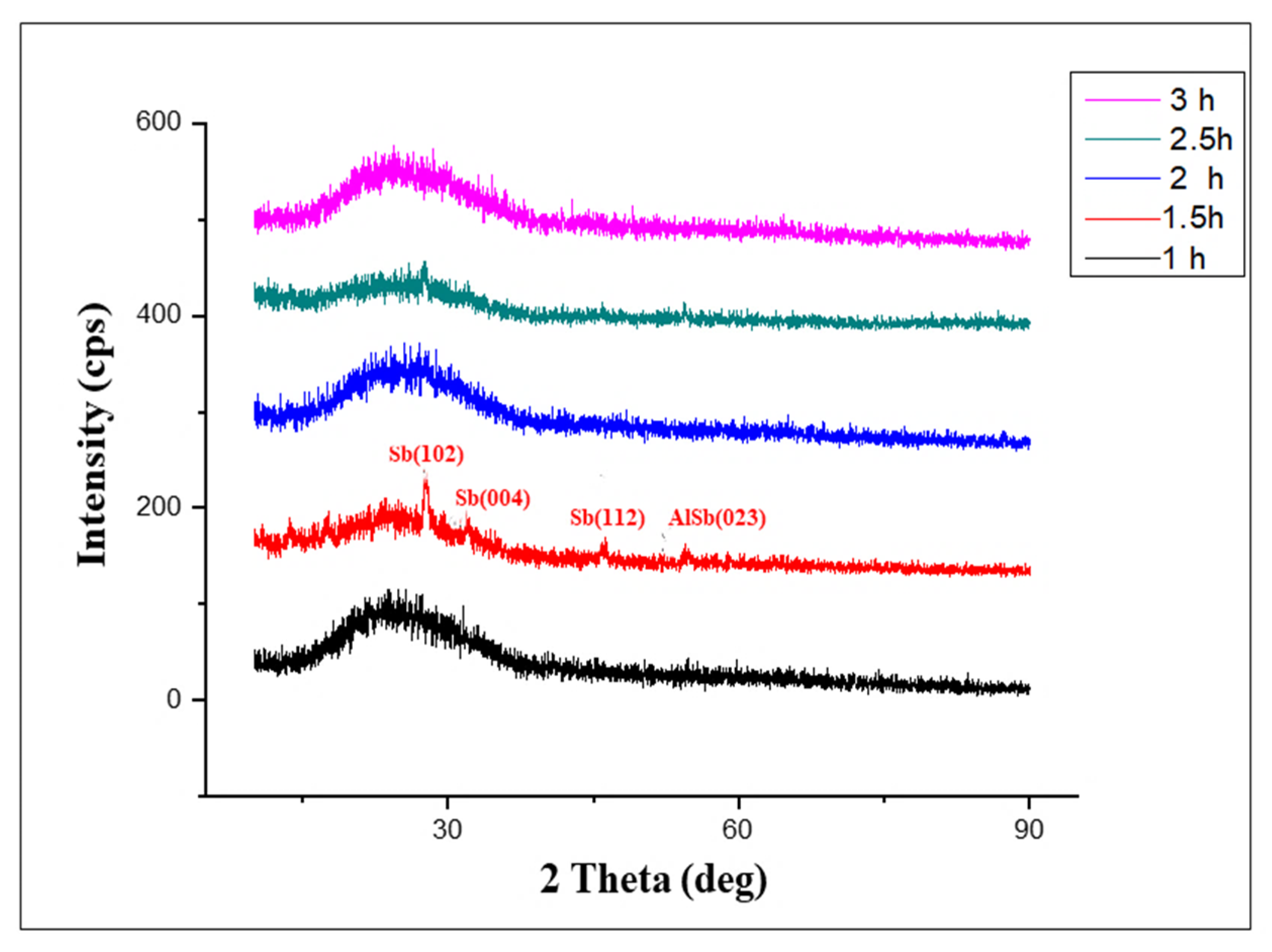
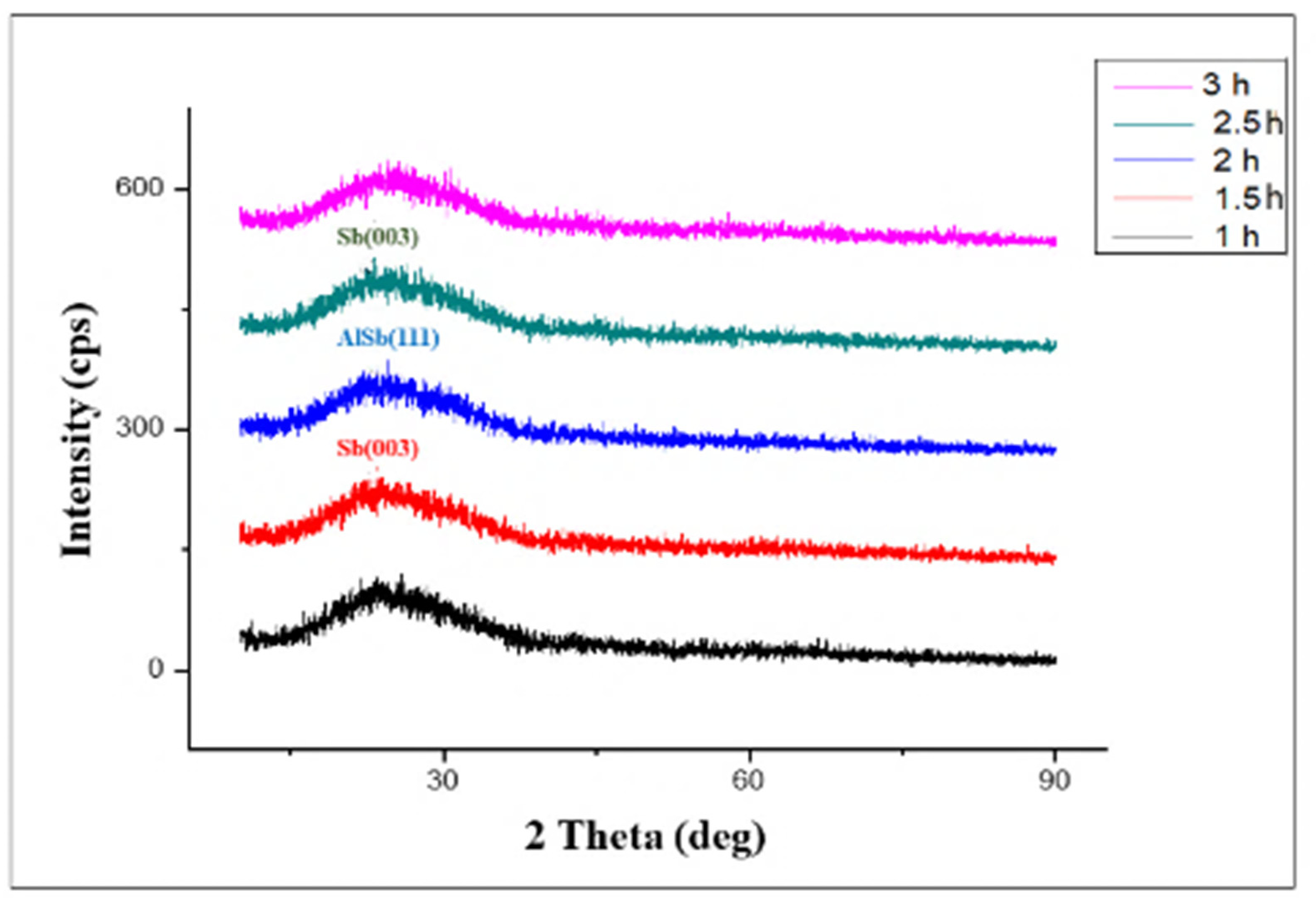
3.1. X-ray Diffraction Analysis

The X-ray diffraction (XRD) technique was used to explore the structural characteristics of the Mg-doped AlSb thin films. The crystallite grain size was calculated by using the Debye-Scherrer formula [16] as:
D = k λ β cos θ
where D represents the crystallite grain size, K = 0.94, wavelength of X-ray source (Cu) λ = 1.54059 A°, β is the full width half maximum (FWHM), which represents the broadening of diffraction line at half of its maximum intensity, and θ represents the Bragg’s angle. In addition, the dislocation line density was estimated using the formula δ = 1/D2 [17].
The XRD patterns of the intrinsic AlSb thin films, which were synthesized by varying the substrate temperature in the range of 72 °C ± 3 °C are illustrated in Figure 1, along with the time variation from 1 to 3 h with a 30-min time step. The graph shows no peak sharpness at time intervals of 1 h, 2 h, 2.5 h, and 3 h, which proved the deposited AlSb thin film was amorphous in nature, while the XRD of the intrinsic AlSb at 1.5 h of deposition time confirmed its polycrystalline nature by the number of peaks observed at various angles along with various planes of reflection. Hence, we will briefly discuss here only the crystalline structures observed at 1.5 h of deposition time. Moreover, the hums present in the peak pattern were due to the glass substrate. These XRD structures and the conclusions drawn from them are consistent with the previous research [1]. Figure 1, showing the XRD patterns of pure AlSb thin films, demonstrates that an AlSb sharp peak was detected at an angle of 54.4° with a plane of reflection value of (023), confirming the cubic structural plan of AlSb thin films [1,18]. The grain size of AlSb film was reported as 0.46 nm, while the dislocation line density peak was measured as 4.6134 × 10¹⁸ m−1 with a d-spacing value of 1.6853 A°. Moreover, the single-crystalline nature of the AlSb thin film was also confirmed by the XRD patterns. Table 1 summarizes the XRD characteristics of pure AlSb for a 1.5-h deposition time along with the Sb data for planes (004), (112), and (102).
Figure 2 demonstrates the 10% Mg-doped AlSb thin film XRD patterns at varying deposition time intervals of 1–3 h. The XRD pattern shows no sharp peaks for the deposition times of 1 h and 3 h, indicating the amorphous nature of AlSb thin films at these times; whereas the results for deposition times of 1.5 h, 2 h, and 2.5 h revealed a number of sharp peaks, indicating the crystalline nature of the doped AlSb films at these time durations, and only these specific deposition times are briefly discussed with reflection planes and other considerable parameters. The XRD parameters summary for the 10% Mg-doped AlSb thin film deposition times of 1.5 h and 2 h is shown in Table 2.
Figure 2 depicts the Sb sharp peak observed at an angle of 23.7° at deposition times of 1.5 h and 2.5 h, as well as the reflection plan at the value of (003), which showed grain sizes of 0.29 nm and 0.23 nm, respectively, depending on the deposition time rate, with a relative intensity of 100% in both cases. However, increasing the deposition time increased the dislocation line density values. In the case of Sb, it was 0.1156 × 10¹⁸ m−1 for 1.5 h of deposition and 0.2015 × 10¹⁸ m−1 for 2.5 h of deposition time, with the d-spacing being the same in both conditions as 3.7515 A°. These findings supported the crystallinity of Sb [19]; whereas the results obtained for AlSb revealed a strong peak at 24.8° with the reflection plan of (111), confirming its cubic structure. The grain size of the synthesized AlSb was 0.22 nm for a deposition period of 2.5 h, with a d-spacing value of 3.5876 A°, which was smaller than Sb but with 100% relative intensity, and these results are consistent with earlier studies [20,21,22,23].

3.2. Surface Morphology

The surface morphology of the intrinsic and 10% Mg-doped AlSb thin films was examined using the MOTIC BA310MET optical microscope from which optical micrographs were computed and are discussed. The surface roughness was computed by using IMAGEJ software (Version IJ 1.46r), which is a Java-based image processing program developed at the National Institutes of Health and the Laboratory for Optical and Computational Instrumentation (LOCI, University of Wisconsin, Bethesda, Maryland) [24].

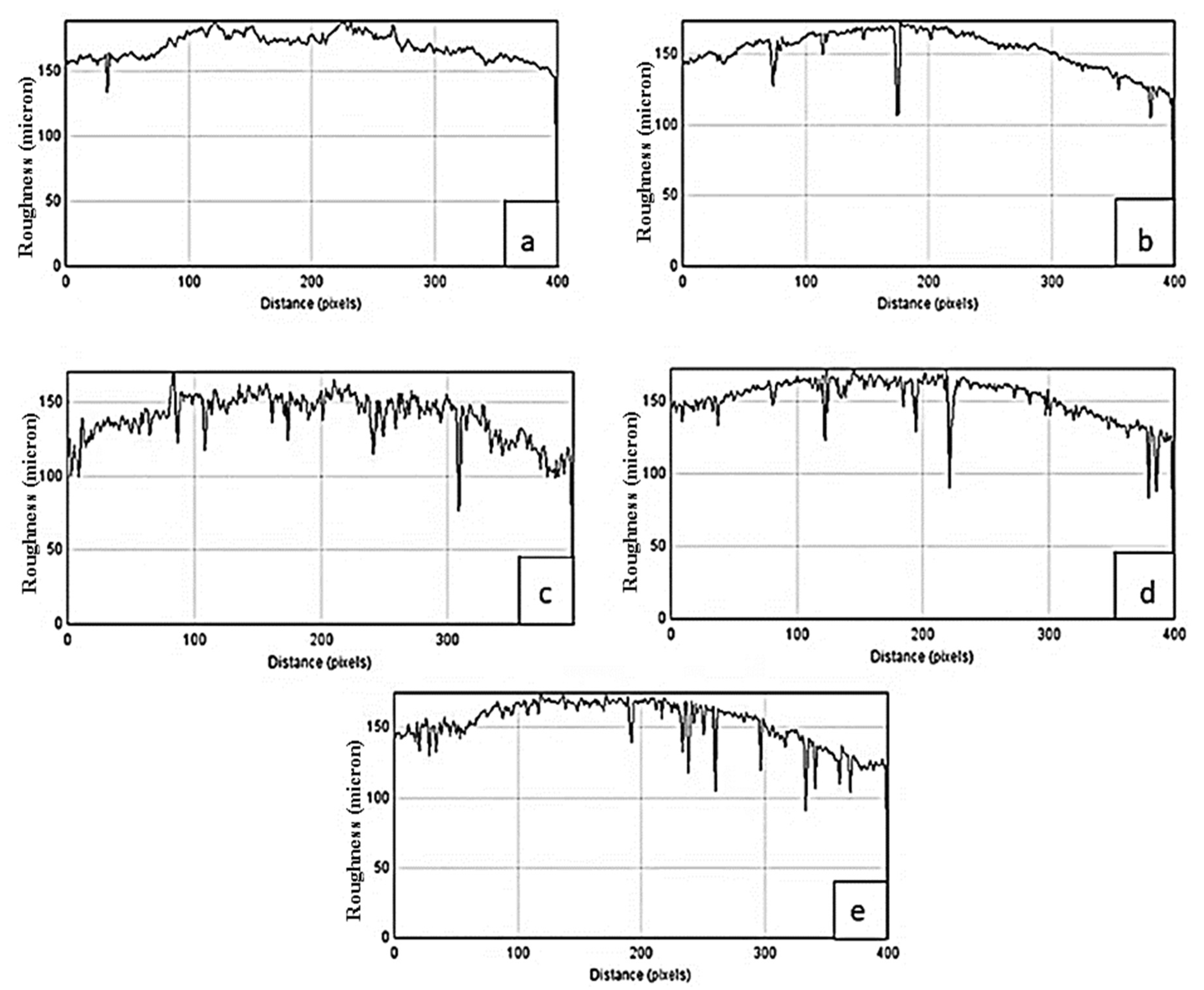
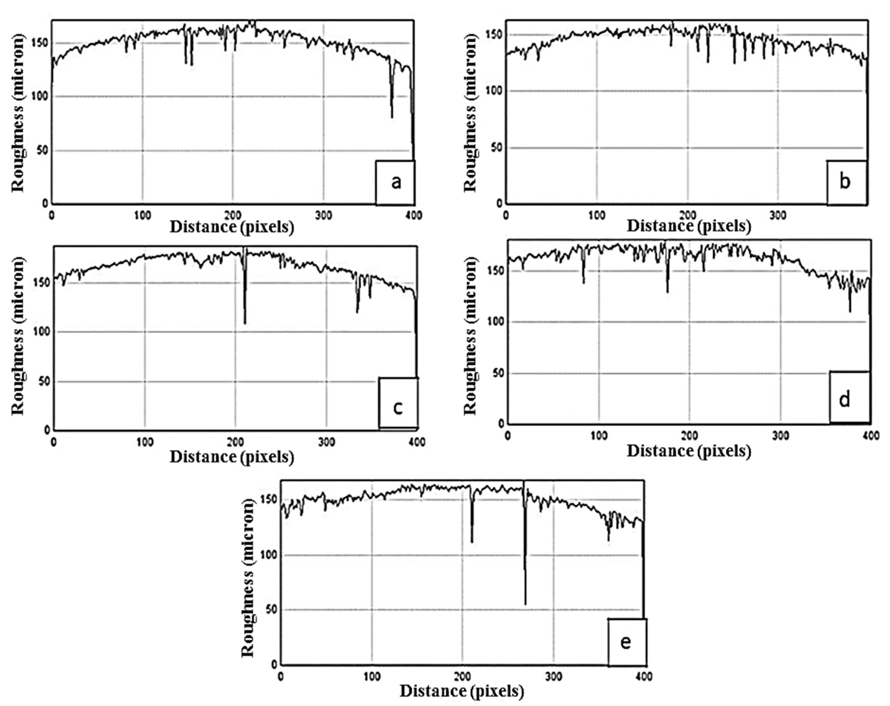
3.2.1. Surface Roughness

The penetration of AlSb and Mg-AlSb compounds on the glass substrate was studied by investigating the optical micrographs using the IMAGEJ software IJ 1.46r across a range of time, which revealed the surface roughness and uniformity of the deposited pure AlSb and Mg-AlSb films. Figure 3 shows the surface roughness of the pure AlSb at deposition times ranging from 1 to 3 h, with the needle shape of peaks defining substrate penetration and the number of needle-shaped peaks displaying the amount of penetration, with more needle-shaped peaks indicating more penetration and thus more surface roughness and nonuniformity. Figure 3a shows no prominent needle peaks at 1-h deposition time, indicating uniform material deposition; whereas Figure 3b shows some needle peaks at 1.5 h, indicating the beginning of penetration; however, Figure 3c,d show a greater number of needle peaks at 2–2.5 h of deposition time, indicating more nonuniformity. After 3 h of deposition (Figure 3e), the penetration achieved its maximum level, as evidenced by maximum needle peaks, demonstrating the nonuniformity of the pure AlSb layer formed on the glass substrate.
Figure 4 shows the surface roughness of 10% Mg-doped AlSb deposited thin films, with Figure 4a showing surface roughness and nonuniformity, which was confirmed by its graph having a number of needle-shaped peaks, and Figure 4b,d showing the same phenomenon with a high number of peaks and thus high surface roughness at 1.5 and 2.5 h, respectively. Figure 4c, on the other hand, shows a smaller number of peaks at a 2-h time interval, but Figure 4e exhibits needle peaks after 3 h of deposition, showing that as the deposition time increased, so did the material penetration, resulting in surface nonuniformity. However, as compared to pure AlSb, the 10% Mg-doped AlSb exhibited fewer needle-shaped peaks, suggesting that the Mg-AlSb had more uniformity and less penetration than pure AlSb, and future device applications will have a better chance as a consequence because of their high uniformity. The tabulated surface roughness data for pure AlSb and 10% Mg-doped AlSb films are shown in Table 3.

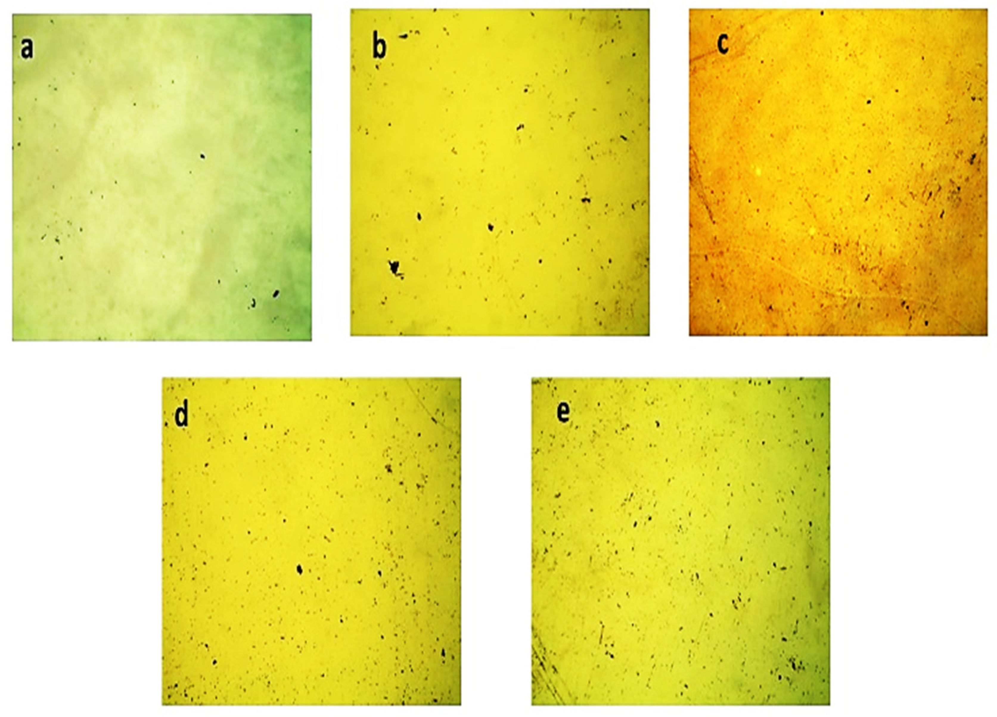
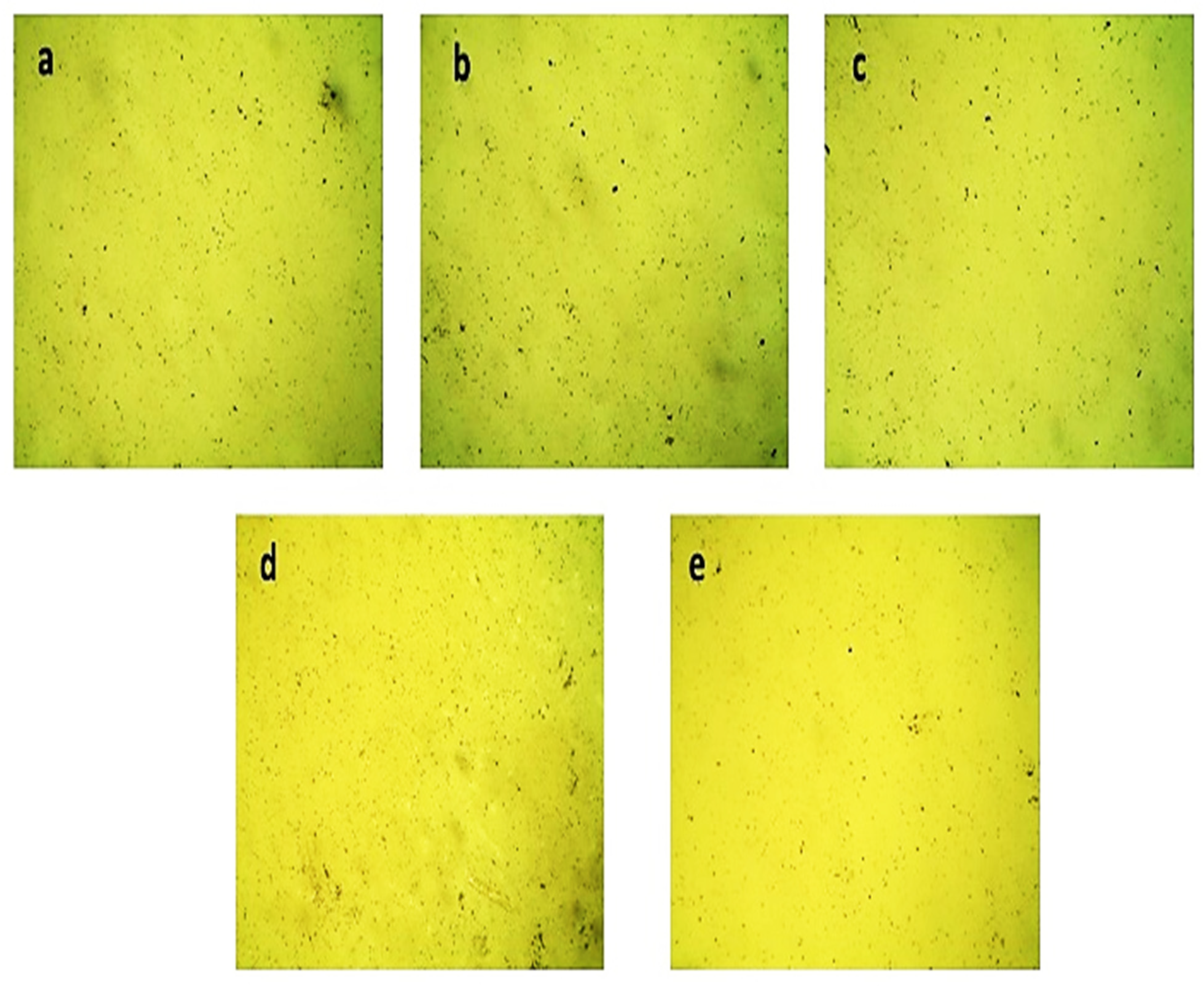
3.2.2. Optical Micrographs

A morphological investigation of pure and Mg-doped AlSb thin films was conducted, yielding information on the deposited film uniformity and surface morphology as a function of deposition time. The film concentration changes were also demonstrated by varying the deposition time factor.
Figure 5 shows the morphological study of the pure AlSb thin films using the optical micrography technique with deposited times ranging from 1 to 3 h, each spaced by 30 min. The pure AlSb is represented by the golden yellow color in all graphs, whereas Figure 5a shows uniform film conformation on the substrate due to less deposition time and material penetration, but some microparticles were still present on the substrate’s surface due to nonhomogeneous entities present in the solution, which resulted in the nonuniformity of film by increasing the deposition time and material penetration. Figure 5b–e, show that the first layer was homogeneous, but the particles on the upper layer were deposited particles that grew as the deposition period increased, affecting the material concentration. These microparticles might be the consequence of Al and Sb precipitates or dust particles in the solution. Furthermore, the particle concentration increased by increasing the film deposition time, which is depicted in Figure 5a–e. With the increase in the deposition time, the nonuniformity of the prepared films increased, depicting an enhanced surface roughness.
The morphological analysis of Mg-doped AlSb, which was the major focus of the current investigation, is shown in Figure 6 with a time range of 1–3 h; once again, the golden yellow colors confirmed the presence of AlSb. Despite the uniformity of the film layers, these optical micrographs contained a number of microparticles, and these microparticles may be due to nonhomogeneous entities present in the solution or to Mg, Al, and Sb precipitates, as well as dust particles in the solution, which created the undesirable effects. The film concentration decreased as the deposition time increased, and vice versa; in general, the films were not uniformly deposited on the substrates, as evidenced by the particles shown in Figure 6a–e, and the greenish color seen in the morphological results confirmed the Mg doping in AlSb films.

4. Conclusions

The most cost-effective approach for synthesizing AlSb thin films was used, and these films were synthesized on a glass substrate using the chemical bath deposition method, which was carried out at various temperatures with a depositing film time ranging from 1 to 3 h. The film formation was examined at each point, and structural, morphological, and surface roughness analyses were conducted at various time intervals. With increasing deposition time, the surface roughness of pure and 10% Mg-doped AlSb increased, causing more material penetration and more nonuniformity. The XRD substantiated the AlSb film formation with its unique structural characteristics in both intrinsic and doped AlSb thin films; whereas, the optical analysis of both pure and doped AlSb thin films proved that the deposition time had a direct relation to the surface roughness. In brief, the results showed that Mg-doped AlSb films had better uniformity with increasing deposition time than their counterparts, having potential applications in photovoltaics, energy, and photonics.

Author Contributions

Conceptualization, S.Z. and M.A.I.; methodology, S.Z. and M.A.I.; software, S.Z.; formal analysis, S.Z., M.M., and M.A.I.; investigations, S.Z. and M.A.I.; resources, S.Z., and M.A.I.; writing—original draft preparation, S.Z., M.M., and M.A.I.; writing—review and editing, S.Z., M.M., M.A.I., W.S., S.I., M.Y.S., J.R.C., and P.V.P.; project administration, M.A.I.; funding acquisition, M.A.I., J.R.C., and P.V.P. All authors have read and agreed to the published version of the manuscript.

Funding

This study was partially supported by the National Research Foundation of Korea (NRF) grant funded by the Korean government (MSIT) (No. NRF-2021R1F1A1062849).

Institutional Review Board Statement

Not applicable.

Informed Consent Statement

Informed consent was obtained from all subjects involved in the study.

Data Availability Statement

All of the data supporting the findings of the presented study are available from the corresponding author on request.

Acknowledgments

M.A.I. acknowledges the support provided by the China Scholarship Council (CSC) from the Ministry of Education of the Peoples Republic of China and Zhejiang University, China.

Conflicts of Interest

The authors declare no conflict of interest.

References

  1. Kareem, T.A.; Kaliani, A.A. X-ray diffraction study of plasma exposed and annealed AlSb bilayer thin film. Plasma Sci. Technol. 2013, 15, 382. [Google Scholar] [CrossRef]
  2. Gandhi, T.; Raja, K.S.; Misra, M. Room temperature electrodeposition of aluminum antimonide compound semiconductor. Electrochim. Acta. 2008, 53, 7331–7337. [Google Scholar] [CrossRef]
  3. Armantrout, G.A.; Yee, J.H. AlSb as a potential photovoltaic material. In Proceedings of the 2nd Photovoltaic Solar Energy Conference, Berlin, Germany, 23–26 April 1979; pp. 960–967. [Google Scholar]
  4. Da Silva, F.W.; Raisin, C.; Nouaoura, M.; Lassabatere, L. Auger and electron energy loss spectroscopies study of the oxidation of AlSb (001) thin films grown by molecular beam epitaxy. Thin Solid Films. 1991, 200, 33–48. [Google Scholar] [CrossRef]
  5. Leroux, M.; Tromson-Carli, A.; Gibart, P.; Vérié, C.; Bernard, C.; Schouler, M.C. Growth of AlSb on insulating substrates by metal organics chemical vapour deposition. J. Cryst. Growth 1980, 48, 367–378. [Google Scholar] [CrossRef]
  6. Das, S.; Ghosh, B.; Hussain, S.; Bhar, R.; Pal, A.K. Pulsed laser deposition: A viable route for the growth of aluminum antimonide film. J. Cryst. Growth 2015, 419, 12–19. [Google Scholar] [CrossRef]
  7. Singh, T.; Bedi, R.K. Growth and properties of aluminium antimonide films produced by hot wall epitaxy on single-crystal KCl. Thin Solid Film. 1998, 312, 111–115. [Google Scholar] [CrossRef]
  8. Tang, P.; Li, B.; Feng, L.; Wu, L.; Zhang, J.; Li, W.; Zeng, G.; Wang, W.; Liu, C. Structural, electrical and optical properties of AlSb thin films deposited by pulsed laser deposition. J. Alloy. Compd. 2017, 692, 22–25. [Google Scholar] [CrossRef]
  9. Shaw, D.; Jones, P.; Hazelby, D. Zinc diffusion in aluminium antimonide. Proc. Phys. Soc. (1958–1967) 1962, 80, 167. [Google Scholar] [CrossRef]
  10. Wieber, R.H.; Gorton, H.C.; Peet, C.S. Diffusion of copper into AlSb. J. Appl. Phys. 1960, 31, 608. [Google Scholar] [CrossRef]
  11. Lili, W.; Shuo, J.; Guanggen, Z.; Jingquan, Z.; Wei, L.; Lianghuan, F.; Bing, L.; Wenwu, W. Cu doped AlSb polycrystalline thin films. J. Semicond. 2013, 34, 013003. [Google Scholar]
  12. Shawon, A.A.; Rahman, M.M.; Ur, S.C. Improvement of Thermoelectric Properties of AlSb by Incorporation of Mg as p-type Dopant. Electron. Mater. Lett. 2020, 16, 540–547. [Google Scholar] [CrossRef]
  13. Rizwan, Z.; Norizam, A.Z.; Sabri, M.G.; Noroozi, M. Characterization of nanostructured CdS film deposited at low growth rate using CBD technique. Chalcogenide Lett. 2010, 7, 423–429. [Google Scholar]
  14. Chan, M.Y.; Lai, S.L.; Fung, M.K.; Lee, C.S.; Lee, S.T. Doping-induced efficiency enhancement in organic photovoltaic devices. Appl. Phys. Lett. 2007, 90, 023504. [Google Scholar] [CrossRef]
  15. Yamasaki, K.; Okada, O.; Inami, K.; Oka, K.; Kotani, M.; Yamada, H. Gallium phthalocyanines: Structure analysis and electro absorption study. J. Phys. Chem. B 1997, 101, 13–19. [Google Scholar] [CrossRef]
  16. Holzwarth, U.; Gibson, N. The Scherrer equation versus the ‘Debye-Scherrer equation’. Nat. Nanotechnol. 2011, 6, 534. [Google Scholar] [CrossRef] [PubMed]
  17. Ham, R.K. The determination of dislocation densities in thin films. Philos. Mag. 1961, 6, 1183–1184. [Google Scholar] [CrossRef]
  18. Shuaib, A.; Khan, M.I.; Bhatti, K.A.; Anwar, A.W.; Dildar, I.M.; Anjum, W. Investigations on structural, morphological and electrical properties of laser irradiated aluminium antimonide. Pak. J. Sci. 2015, 67, 191–197. [Google Scholar]
  19. Inbakumar, S. Optical and structural analysis of plasma-treated and annealed Al–Sb bilayer thin films. Ionics 2009, 15, 191–195. [Google Scholar] [CrossRef]
  20. Zheng, H.; Li-Li, W.; Bing, L.; Xia, H.; Jian-Xiong, H.; Liang-Huan, F.; Wei, L.; Jing-Quan, Z.; Yap-Ping, C. The electrical, optical properties of AlSb polycrystalline thin films deposited by magnetron co-sputtering without annealing. Chin. Phys. B 2010, 19, 127204. [Google Scholar]
  21. Chen, W.; Feng, L.; Lei, Z.; Zhang, J.; Yao, F.; Cai, W.; Cai, Y.; Li, W.; Wu, L.; Li, B.; et al. AlSb thin films prepared by DC magnetron sputtering and annealing. Int. J. Mod. Phys. B 2008, 22, 2275–2283. [Google Scholar] [CrossRef]
  22. He, J.; Wu, L.; Feng, L.; Zheng, J.; Zhang, J.; Li, W.; Li, B.; Cai, Y. Structural, electrical and optical properties of annealed Al/Sb multilayer films. Sol. Energy Mater. Sol. Cells 2011, 95, 369–372. [Google Scholar] [CrossRef]
  23. Sattar, F.; Shahid, W.; Anwar, A.W.; Iqbal, M.A.; Malik, M.; Anwar, N.; Idrees, F.; Din, S.Z.; Kanwal, Q. Synthesis and characterization of Zn doped AlSb thin films for photovoltaic and energy applications. Z. Für Nat. A 2022, 77, 507–513. [Google Scholar] [CrossRef]
  24. Schneider, C.A.; Rasband, W.S.; Eliceiri, K.W. NIH Image to ImageJ: 25 years of image analysis. Nat. Methods 2012, 9, 671–675. [Google Scholar] [CrossRef] [PubMed]
Figure 1. XRD patterns of pure AlSb thin films for 1–3 h.
Applsci 12 07412 g001
Figure 2. XRD patterns of 10% Mg-Doped AlSb thin films for 1–3 h.
Applsci 12 07412 g002
Figure 3. Surface roughness of pure AlSb at different deposition times (a) 1 h, (b) 1.5 h, (c) 2 h, (d) 2.5 h, and (e) 3 h.
Applsci 12 07412 g003
Figure 4. Surface roughness of 10% Mg-doped AlSb films at different deposition times (a) 1 h, (b) 1.5 h, (c) 2 h, (d) 2.5 h, and (e) 3 h.
Applsci 12 07412 g004
Figure 5. Pure AlSb-deposited thin films’ optical micrographs for time durations of (a) 1 h, (b) 1.5 h, (c) 2 h, (d) 2.5 h, and (e) 3 h.
Applsci 12 07412 g005
Figure 6. Mg-doped AlSb-deposited thin films’ optical micrographs for time durations of (a) 1 h, (b) 1.5 h, (c) 2 h, (d) 2.5 h, and (e) 3 h.
Applsci 12 07412 g006
Table 1. The XRD data of pure AlSb-deposited thin films recorded at 1.5 h.
Peak No.2θ (Degree)D (A°)HklIntensity (I)FWHMG.S (nm)Dislocation Line Density
(m−1 × 10¹⁸)
154.41.6853(023)54.40.6250.464.6134
227.73.2182(102)27.70.780.622.5407
332.12.7864(004)32.10.770.190.2739
446.21.9635(112)46.20.6250.490.4039
Table 2. The XRD data of 10% Mg-doped AlSb deposited thin films at 1.5 and 2 h.
Peak No.2θ (Degree)D (A°)HklIntensityFWHMGrain Size (nm)Dislocation Line Density
(m−1 × 10¹⁸)
1.5 h Deposition Time
123.73.7515(003)23.70.6250.290.1156
2 h Deposition Time
124.83.5876(111)24.80.620.220.1946
223.73.7515(003)23.70.8250.230.2015
Table 3. Surface roughness of pure and Mg-doped AlSb thin films at different deposition times.
Sr. No.Distance
(Pixels)
Roughness (Microns) at Deposition Time (s)
6090120150180
Pure AlSb thin films
175136136139167134
2150165164166172167
322518916914689153
4300138147161159152
53751311199881112
10% Mg-doped AlSb thin films
175142154182139149
2150129151163173174
3225158127112151166
4300151144177159150
537582137147113124
Publisher’s Note: MDPI stays neutral with regard to jurisdictional claims in published maps and institutional affiliations.

