Review

Inverse Design for Silicon Photonics: From Iterative Optimization Algorithms to Deep Neural Networks

1
Tsinghua-Berkeley Shenzhen Institute, Tsinghua University, Shenzhen 518055, China
2
Tsinghua Shenzhen International Graduate School, Tsinghua University, Shenzhen 518055, China
3
School of Electronic and Computer Engineering, Peking University, Shenzhen 518055, China
*
Author to whom correspondence should be addressed.
Appl. Sci. 2021, 11(9), 3822; https://doi.org/10.3390/app11093822
Submission received: 22 March 2021 / Revised: 8 April 2021 / Accepted: 14 April 2021 / Published: 23 April 2021
(This article belongs to the Special Issue Nanophotonic Devices and Technologies)

Abstract

:
Silicon photonics is a low-cost and versatile platform for various applications. For design of silicon photonic devices, the light-material interaction within its complex subwavelength geometry is difficult to investigate analytically and therefore numerical simulations are majorly adopted. To make the design process more time-efficient and to improve the device performance to its physical limits, various methods have been proposed over the past few years to manipulate the geometries of silicon platform for specific applications. In this review paper, we summarize the design methodologies for silicon photonics including iterative optimization algorithms and deep neural networks. In case of iterative optimization methods, we discuss them in different scenarios in the sequence of increased degrees of freedom: empirical structure, QR-code like structure and irregular structure. We also review inverse design approaches assisted by deep neural networks, which generate multiple devices with similar structure much faster than iterative optimization methods and are thus suitable in situations where piles of optical components are needed. Finally, the applications of inverse design methodology in optical neural networks are also discussed. This review intends to provide the readers with the suggestion for the most suitable design methodology for a specific scenario.

1. Introduction

Silicon photonics enables massive fabrication of integrated photonic devices at low cost, due to its compatibility with complementary metal oxide semiconductor (CMOS) process [1]. It has emerged as one of the most important technologies for data communication [2] and computations [3], as integrated electronic circuits are reaching their limits as well as incurring high energy costs. Recently, it has also shown the potential for other applications such as sensing [4] and light detection and ranging (LiDAR) [5]. For miscellaneous silicon photonic devices, their versatile functions mainly come from design of device geometry [6]. Intuitively, the design of single component with specific function is fulfilled by physics-based methods like analytical models, prior practical experiences and scientific intuitions [7]. However, the physics-based methods are laborious and have high requirements on designers’ experience. Furthermore, the performance evaluation of light-material interaction with complicated geometries has to rely on numerical electromagnetic (EM) simulations [8], as the computation for irregular geometry is often non-intuitive. To make the design process more efficient, inverse design approaches have been introduced, which are assisted by various iterative optimization methods and deep neural networks (DNNs) [6,7,8,9,10,11,12].
Iterative optimization algorithms can optimize device geometric parameters for targeted optical performance. They have been widely researched recently due to their time-efficiency and satisfactory optimization results. For devices with regular structure, key geometry parameters, which suggest the degrees of freedom (DOF) during design, are abstracted and tuned for targeted optical performance. For devices with one or two DOF, the optimal optical performance can be found by sweeping all the possible solutions. However, the sweeping process would be extremely laborious and require large time budget for higher DOF, as EM simulations are time-consuming. The relationships between geometry parameters and optical performance are quite similar to mathematical non-deterministic polynomial hard (NP-hard) problems [13] which are difficult to define by explicit function. Inspired by iterative gradient-free algorithms such as genetic algorithm (GA), particle swarm optimization (PSO) and direct binary search (DBS) for solving NP-hard problems, lots of regular silicon photonic devices are optimized in these ways [14]. Apart from gradient-free algorithms, gradient-based algorithms like topology optimization (TO) for devices with irregular structure have also been investigated for inverse design recently [15]. Instead of abstracting key parameters that describes device geometry, TO takes the whole design space as a bitmap, where all the pixels are iteratively updated towards the direction of gradient descent until the gradients are small enough. In this way, complex geometric pattern could be quickly generated for a targeted optical performance.
The iterative optimization algorithms discussed above could optimize only one device for one-round optimization and the whole optimization process has to be repeated again when the optical response target varies a little. This is extremely laborious when many similar devices are needed with slightly difference target response, such as power splitters with different splitting ratios or grating couplers (GCs) working at different wavelength bands [16]. Fortunately, DNN, an unprecedented tool capable of building a bridge between data features and data labels, has also found its way to assist the design of silicon photonic devices [6]. Based on the mapping direction between geometric parameters and optical response, DNNs are trained as forward models and inverse models. A forward model maps geometric parameter of a device to its optical response. It surrogates EM solvers to accelerate device performance evaluation in optimizations. On the contrary, an inverse model maps desired optical response to geometric parameters. It takes almost no time to generate a device for a specific demand after the model is well-trained, eliminating the need for optimizations.
There are already some excellent review papers about optimization algorithms and DNNs for nanophotonics inverse design. For example, Molesky et al. focused on the adjoint method and its applications [7] and Jensen et al. concentrated on topology optimization of nanophotonics [15]. More recently, Jiang et al. and So et al. presented very detailed reviews about DNNs-assisted metasurface and nanophotonics design [6,8]. Different from these previous reviews, we review design methodologies for silicon photonics from the perspective of demands. According to different design goals for a single device or multiple similar devices, we separate the design methodologies into iterative optimization algorithms and DNNs-assisted methods. The iterative optimization algorithms are illustrated in the sequence of increased DOF: empirical structure, QR-code like structure and topology structure. We also separate DNNs into discriminative neural networks and generative neural networks which are trained as forward models and inverse models, respectively. Finally, we point out the challenges of existing design methodologies and highlight a future research direction: inverse designed optical neural networks (ONN).

2. Inverse Design of Silicon Photonics with Iterative Optimization Algorithms

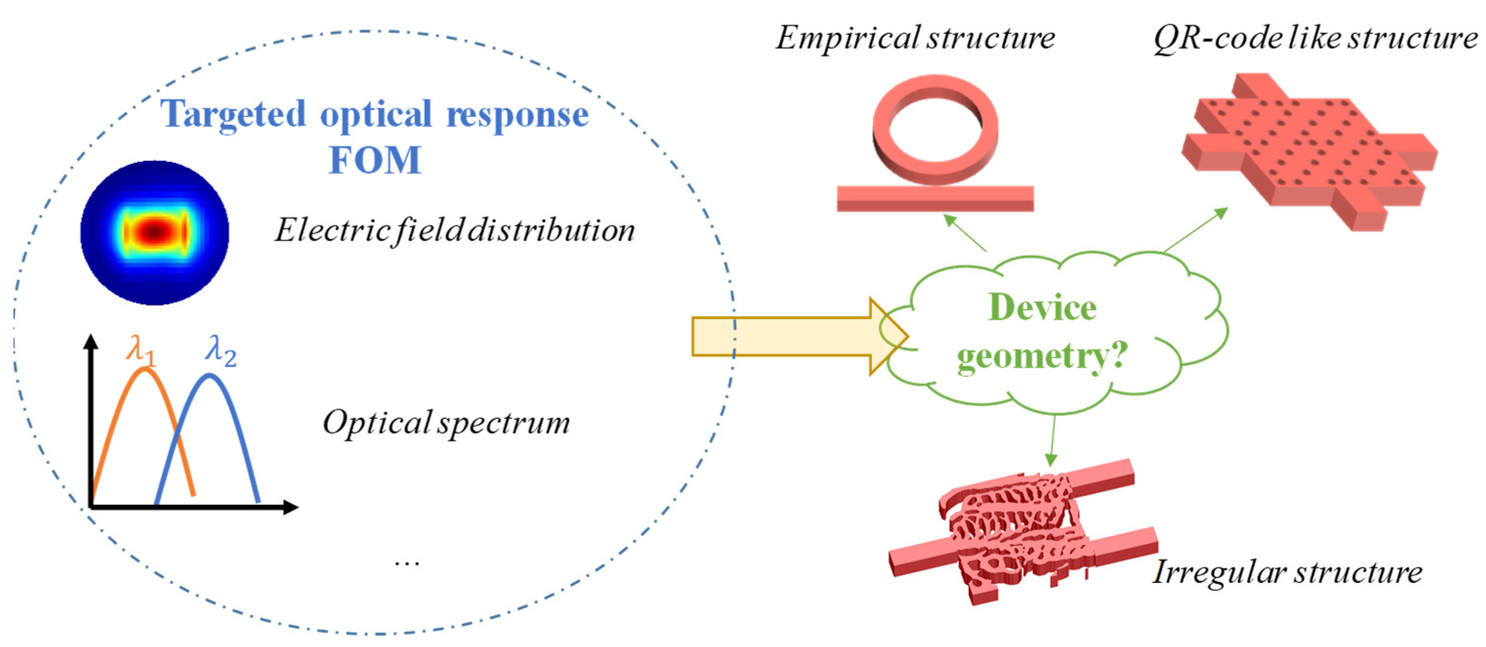
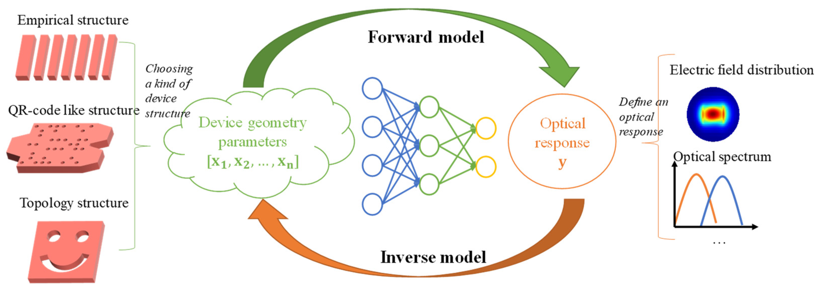
2.1. Inverse Design Schemes for Silicon Photonics

Different from electronic circuits where the versatile functions come from the combination of electronic components, a single silicon photonic device is able to achieve complex functions with delicate geometry design. For the given geometry of a device, its optical response can be evaluated by EM simulation before experimental validation. EM simulation tools have been developed by solving Maxwell’s equations numerically. These tools are important for device modelling and optimization, by allowing the designer to understand how light propagates in a given geometry and to obtain an accurate optical response. Widely adopted EM simulation methods include finite element method (FEM) [17], finite-difference time-domain method (FDTD) [18], eigenmode expansion method (EME) [19] and rigorous coupled wave analysis (RCWA) [20]. The FDTD method is among the most popular choices for silicon photonic device since it is a general EM solver well suited for high index contrast structures with complex geometry. It also allows wideband simulation as spectral response is generally needed for silicon photonic devices.
For a targeted optical response, inverse design tries to find a suitable device geometry. As shown in Figure 1, either a certain electric field distribution or an optical spectrum could serve as the figure of merit (FOM) which describes the phenomenon of interest to the designer. Other merits such as performance, compactness or fabrication feasibility may also be considered for different application scenarios. Based on the number of DOF, three types of structures are widely used for inverse design: empirical structure [21,22,23,24,25,26,27,28,29,30,31,32], QR-code like structure [33,34,35,36,37,38,39,40,41,42,43,44,45] and irregular structure [46,47,48,49,50,51,52,53,54,55,56,57,58]. An empirical structure making use of existing classical structures usually has only a few DOF. A QR-code like structure with hundreds of DOF selectively etches the design area with regular shapes such as rectangles or circles in a periodic manner. An irregular structure taking the whole design area as a bitmap has the most complex pattern with hundreds of thousands DOF. In the rest of this section, iterative optimization algorithms for optimizing these structures are illustrated and compared in detail.

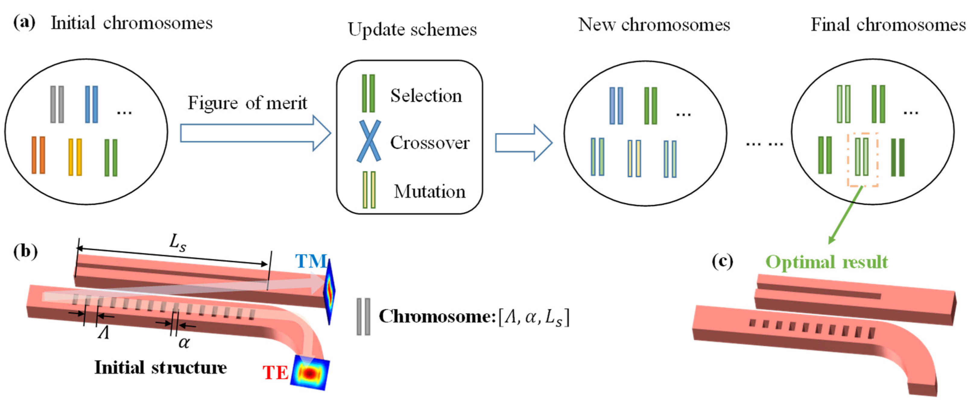
2.2. Optimization of Empirical Structures

An empirical structure makes use of classical structures, where only a few parameters like radius, duty cycle, widths of waveguides, etc. are tuned for targeted optical response. These classical structures are proposed by researchers for different application scenarios. For example, micro-rings are preferred for wavelength selection due to their high wavelength-sensitivity [21,27]. Directional couplers (DCs) are used for polarization beam splitters (PBS), mode-division multiplexers (MDM) and wavelength-division multiplexers (WDM) since DCs couple light from one waveguide to another in a reciprocating way [21,24,26]. Y-splitter with three ports is widely used for power splitting (PS) [59]. Mach-Zehnder interferometer (MZI) can separate light and finally combine with optical path difference, so that it could be utilized for optical switches or modulators [30,60,61]. Gratings which periodically arrange the silicon and air (or silica) have been applied to manipulate the effective refractive index of waveguides or act as fiber grating couplers (GC) [62,63]. With known structures and underlying theories to design a device for targeted FOM, it still costs lots of time to tailor the key parameters, as each parameter set requires at least one EM simulation.
The relationship between the abstracted key parameters from an empirical structure and its optical response is a kind of NP hard problem, which can be solved by heuristic algorithms. GA, a kind of heuristic optimized algorithm, is inspired by Darwinian evolution theory of survival of the fittest [64]. After initial chromosomes, which represent different parameter sets, are randomly generated, the fitness values describing the FOM of each chromosome are computed as shown in Figure 2a. Chromosome with better fitness values will be chosen as elite and passed to the next generation directly. For the rest of chromosomes, some chromosomes experience crossover with others to create new chromosomes and some produce offspring by mutation. Through the above elite selection, crossover and mutation, a new generation is born. This procedure is repeated until the best FOM is found.
We take reference [25] for example to illustrate utilizing GA to optimize an optical device with empirical structure. A broadband PBS based on directional coupler and subwavelength gratings (SWGs) structure is designed as shown in Figure 2b. Key parameters like pitch Λ , duty cycle α and coupling length L s are abstracted to represent this structure and coded as a chromosome. Initial chromosomes (20 parameters sets) are generated randomly within parameter boundaries. The FOM of each chromosome is calculated with respect to the output of transverse electric (TE) mode at through waveguide and transverse magnetic (TM) mode at cross waveguide. After hundreds of iterations, the best parameter set is found as Figure 2c suggests, where the transmission efficiencies for both TE and TM modes at desired output ports are larger than 85% over wavelength range from 1250 nm to 1680 nm.
Another popular heuristic algorithm is PSO [65]. Different form GA, where parts of parameter sets are updated at each iteration, PSO updates all the parameter sets towards the global optimized FOM. For PSO, the initial randomly generated parameter sets are called particles, each of which is assigned an initial velocity. PSO evaluates the FOM of each particle and finds the best global and local FOMs as well as the corresponding particles. According to the global best particle and the local best particle at their current iteration, the velocity of each particle is updated. With updated velocities, the new population are generated from original particles. This updating procedure is repeated until the global best FOM is converged to an acceptable value. PSO has also been widely used for the design of silicon photonic devices with empirical structures as listed in Table 1.

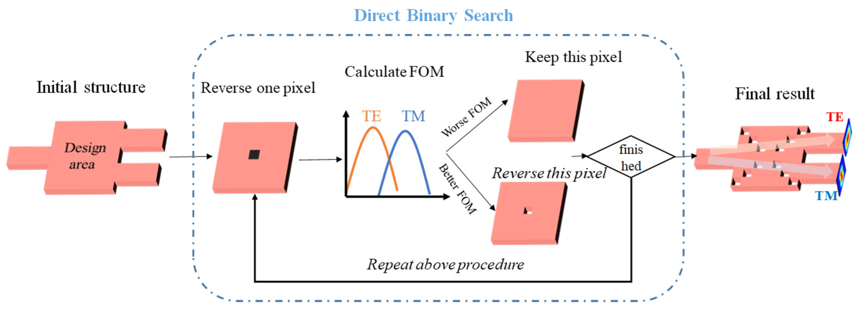
2.3. Optimization of QR-Code like Structures

A QR-code like structure, where regular shapes like circles or rectangles are selectively etched on a periodic 2-D surface, is also an important approach for manipulating light propagation in waveguides. Different from empirical structure-based design, QR-code like structure with hundreds of DOF is a more general approach for different problems. In a QR-code like structure, designers only have to define the pitch and size of etched holes as well as the footprint of design area. For each hole, to be etched or not is determined automatically to achieve better FOM. Using a compact QR-code like structure, many different functional components like power splitter [41,45], polarization rotator [33,42,44], PBS [40], WDM [42], MDM [34,39], crossing [66], GC [67] and photonic crystal [68] have been designed.
DBS, a brute-force searching algorithm, initially proposed by Seldowitz et al. for the synthesis of digital holograms [69], has been proven to be efficient for the design of devices with QR-code structure. Shen et al. introduced DBS to design a very compact integrated PBS on SOI platform [40], as shown in Figure 3. They defined the size of design area to be 2.4 × 2.4 μm2 with each hole size to be 0.12 × 0.12 μm2. There are 400 rectangular pixels to determine whether to etch or not. During each iteration, one pixel in the design area is reversed and the FOM (average transmission efficiency of TE and TM modes at the targeted output ports) is calculated and compared with the FOM for last iteration. If the new FOM is larger than the old one, the new geometry with reversed pixel is past to the next generation, otherwise, the old geometry is kept. The above procedure is repeated until the FOM is large enough to be acceptable. After about 140 h of optimization, the average transmission efficiency of optimized PBS is higher than 70% and its 1 dB bandwidth is 83 nm.
In addition to DBS, heuristic algorithms like GA and PSO have also been applied for the design of integrated silicon photonic devices based on QR-code like structure. Different from DBS, which updates one pixel at each iteration, heuristic algorithms code all the pixels as an individual and update them together during each iteration, hence the total number of iterations could be reduced.

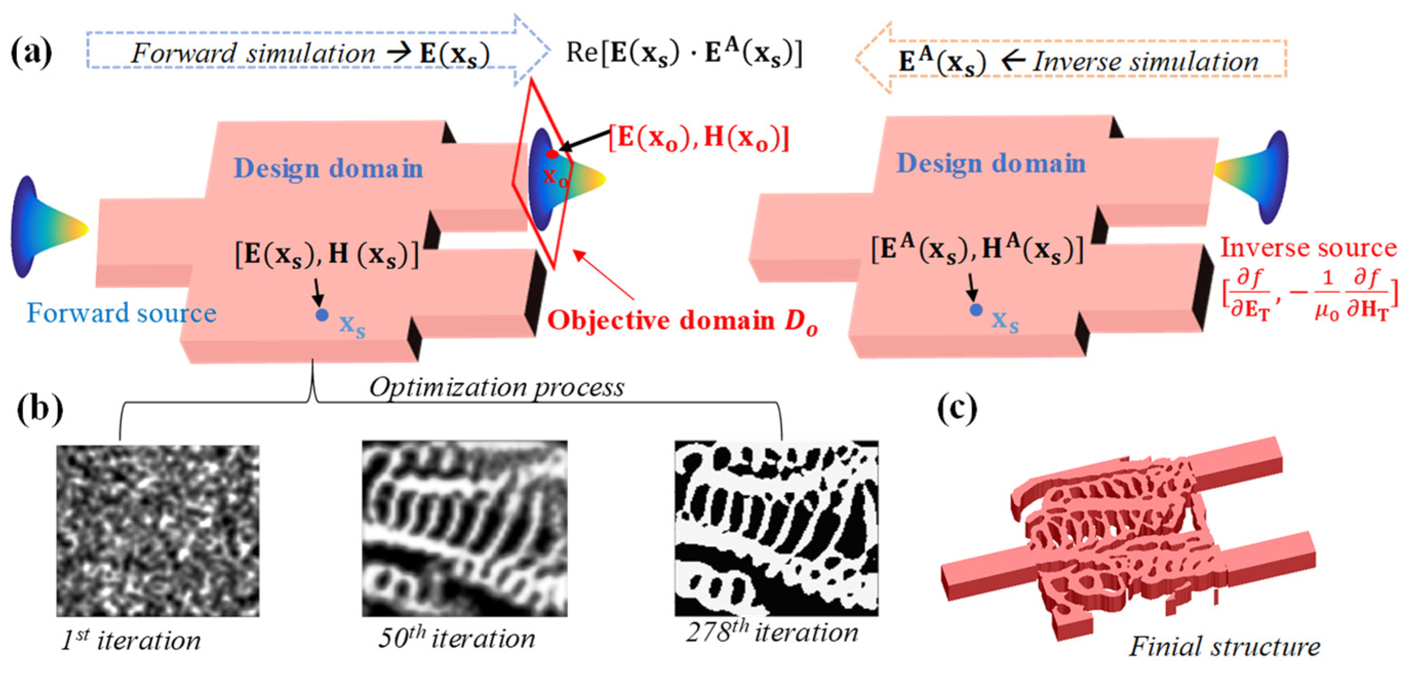
2.4. Optimization of Irregular Structures

An irregular structure owns the highest DOF since the whole design area is segmented into very small pixels [15]. Different from QR-code like structure which also pixelates the design area with 100 or 200 nm resolution, an irregular structure is more intricate with ultra-high resolution (10 or 20 nm scale). It would be extremely time-consuming for gradient-free algorithms discussed above to optimize an irregular structure with thousands of DOF, as the required simulations is proportional to the number of DOF. Fortunately, gradient-based algorithms cast light on this time-consuming problem, where all the parameters are updated with the fewest simulations.
To describe the optimization process, a mathematical model which tries to optimize the FOM at the constraints of Maxwell equations is built as in Equation (1):
max ϵ , μ F ( E , H ) s . t .   { · ϵ E = ρ · μ H = 0   × E = j ω μ H × H = J + j ω ϵ E   ,
where FOM F ( · ) is the function of electric field E and magnetic field H . Permittivity ϵ and permeability μ in the design area are variables to be tuned for better FOM. Objective-first (OF) method [56] and topology optimization (TO) with adjoint method [70] have been proposed to solve Equation (1).
We take irregular PBS in reference [71] as an example to illustrate the TO process. As shown in Figure 4a, the design domain D s is optimized by adjoint method for two FOMs. The first FOM is the transmission of TE mode at the upper arm while the second FOM is the transmission of TM mode at the lower arm.
As the optimization processes of two arms are similar, we only give detailed derivation of TE mode here. In the objective domain D o , the actual EM fields are optimized towards fundamental TE mode. The targets at each position x o in the objective domain is defined in the form of Poynting vectors [70] as in Equation (2):
f ( E ( x o ) , H ( x o ) ) = E ( x o ) × H T ( x o ) ¯ + E T ( x o ) ¯ × H ( x o ) ,
where E , H are the actual EM fields from the simulation, and E T ¯ ,   H T ¯ are the constant conjugated EM fields of the fundamental TE mode. The best target f ( E ( x o ) , H ( x o ) ) requires the value of actual EM fields to be the largest and the direction of actual EM fields to be the same with fundamental TE mode at position x o . However, it is still hard to determine whether the FOM is good or not when some positions get better targets while others get worse. Therefore, the total FOM is defined as the integral of all the targets in the objective domain as in Equation (3):
F ( E , H ) = D o f ( E ( x o ) , H ( x o ) ) d 3 x o .
The derivative of total FOM to permittivity and permeability in the design domain D s is calculated using chain rule. Firstly, the derivative of total FOM to actual EM fields in the objective domain D o is calculated as in Equation (4):
δ F ( E , H ) = 2 Re D o [ f E ( x o ) δ E ( x o ) + f H ( x o ) δ H ( x o ) ] d 3 x o ,
where factors f E ( x o ) ,   f H ( x o ) are the constant values and are easy to get from Equation (2) as in Equation (5):
f E ( x o ) = n ^ E × H T ( x o ) ¯ f H ( x o ) = E T ( x o ) ¯ × n ^ H .
However, the terms δ E ,   δ H cannot be calculated analytically, as the relationship between E , H at objective domain and ϵ ,   μ at design domain cannot be expressed by an explicit function. Since the variation of permeability δ μ causes little change to EM fields, only the variation of permittivity δ ϵ is considered. In the design domain, the original geometry has electric field E ( x s ) at x s . When a very small volume V at this position has a small permittivity change δ ϵ , this will cause an induced dipole moment p i n d ( x s ) = V ϵ 0 σ ϵ E ( x s ) . Numerically, EM field variation δ E ( x o ) ,   δ H ( x o ) at x o in the objective domain come from the summation effects of this induced dipole moments in the design domain, which can be expressed with Green’s function [72] as in Equation (6):
δ E ( x o ) = ds G E P ( x o , x s ) p i n d ( x s ) d 3 x s δ H ( x o ) = d s G H P ( x o , x s ) 1 μ p i n d ( x s ) d 3 x s ,
where G E P ( x o , x s ) and G H P ( x o , x s ) represent the EM fields at x o in the objective domain from a unit dipole at x s in the design domain. The symmetry theory suggests the following relation as in Equation (7):
G E P ( x o , x s ) = G E P ( x s , x o ) G H P ( x o , x s ) = G H P ( x s , x o ) .
By substituting Equations (6) and (7) into Equation (4) and making an equivalent transformation, we get the total FOM as in Equation (8):
F ( E , H ) = ϵ 0 δ ϵ V D s d 3 x s E ( x s ) 2 Re D o d 3 x o [ G E P ( x s , x o ) f E ( x o ) G H P ( x s , x o ) f μ H ( x o ) ] .
The inner integration is defined as the “adjoint” electric field E A ( x s ) at position x s in design domain as in Equation (9):
E A ( x s ) = D o d 3 x o [ G E P ( x s , x o ) · f E ( x o ) + G H P ( x s , x o ) · ( f μ H ( x o ) ) ] .
This adjoint electric field E A ( x s ) can be obtained through the integration of all induced electric fields which come from EM dipoles with amplitudes [ f E ( x o ) , f μ H ( x o ) ] at different positions x o at the objective domain. These amplitudes are constant values which are calculated by using Equation (5). Through an “inverse” simulation, where light source with amplitude [ f E , f μ H ] is placed in objective domain, all the adjoint fields in design domain can be numerically calculated. Substituting Equation (9) into Equation (8), the derivative of total FOM in the objective domain to permittivity ϵ s in the design domain is shown in Equation (10):
δ F ( E , H ) δ ϵ s = ϵ 0 V Re [ E ( x s ) E A ( x s ) ] .
With one forward simulation which calculates all the electric fields E ( x s ) and one inverse simulation which computes all the adjoint electric fields E A ( x s ) in the design domain, the derivatives of total FOM to all the permittivity ϵ s can be obtained as Equation (10) suggested. As discussed before, there are two FOMs for PBS. For another FOM’ which tries to guide TM mode to the second waveguide arm, the derivative of FOM’ to permittivity ϵ s in the design domain is also calculated in similar way. The permittivity in the design domain is updated towards the direction of total gradient decent as in Equation (11):
ϵ s n e w = ϵ s o l d + α ( δ F δ ϵ s + F ϵ s ) ,
where α is the updating rate. The updating process is repeated until the gradient is small enough.
During the updating process, permittivity ϵ s is taken as a continuous variable for convenience of derivative calculation, which has to be discretized for real application scenarios. Both level-set [73] and density optimization [74] have been applied for discretization. In silicon platform, the design domain usually composes of silicon and silica (or air) with permittivity ϵ 1 and ϵ 2 , respectively. The level-set method defines a continuous variable φ s with values ranging from negative to positive. φ s = 0 suggests the boundary between two materials and the discrete permittivity in the design domain is defined as in Equation (12):
ϵ s = { ϵ 1 , φ s 0 ϵ 2 , φ s < 0 .
On the other hand, for density method, the values of continuous variable φ s range from 0 to 1, and the permittivity in the design domain is expressed as in Equation (13):
ϵ s = ϵ 2 + φ s ( ϵ 1 ϵ 2 ) .
Different from level-set method which is discretized after applying Equation (12), the density method would generate “gray structures” with continuous permittivity between ϵ 1 and ϵ 2 . To further discretize permittivity, Su et al. proposed a discretization method by introducing self-biasing or neighbor-biasing [46]. In the example of PBS design, density method is adopted and the optimization process is shown in Figure 4b, where an initial random structure is finally optimized and discretized after 278 iterations.
Apart from discretization of permittivity, minimal feature size control is also an important issue for irregular structures as the large DOF bring features with critical size too small to be fabricated. Different approaches are proposed to solve this issue, such as density filters [75], penalty functions [76], artificial damping [50] and morphological filters [77]. Recently, Khoram et al. introduced b-splines to control minimal feature size of irregular structures [78]. Instead of filtering out small features directly, this method transfers the design domain to lower space dimension composed of b-spline functions, which damps small features internally. In the example of PBS design, the optimized device geometry is shown in Figure 4c, where density adjoint method with b-spline function is adopted. Within the footprint of 2.4 × 2.8 μm2, this optimized PBS splits TE and TM modes with over 90% transmission efficiency covering 420-nm wavelength range.

2.5. Comparison of Iterative Optimization Algorithms for Silicon Photonics Design

We have discussed three examples of inverse designed PBSs via different initial structures with corresponding iterative optimization algorithms in the above three subsections. The PBS based on empirical structure has high transmission efficiency (over 85% within 420 nm wavelength range) for both TE and TM modes and the critical size is under the control of designers. However, it also has the largest footprint (approximately 7 × 4 μm2) and the lowest DOF (only 3). It takes about one week to optimize this device on two 12-core central processing units (CPUs). Profound prior knowledge about the coupling theory is also required and a skillful initial structure has to be chosen, otherwise, the device may not work at all. The PBS based on QR-code like structure has ultra-compact size (2.4 × 2.4 μm2) as well as high DOF (i.e., 400). Its design process does not need much prior knowledge but the optimization time is long (~140 design hours) as each QR-code has to be verified during DBS. This time-consuming optimization process limits both the size of footprint and the number of DOF, so the transmission efficiency of DBS optimized PBS is not very high. The peak efficiency of optimized PBS is ~80% and its 1 dB bandwidth is 83 nm. The irregular PBS optimized via adjoint method is also ultra-compact (2.8 × 2.4 μm2), and it has 16,800 DOF due to its ultra-high resolutions (i.e., 20 nm). After 64 h of optimization on two 12-core CPUs, the final irregular PBS has transmission efficiency over 90% covering 420-nm wavelength range. The irregular PBS has a time-efficient optimization process, where all the parameters can be updated in one round via only two simulations (one forward simulation and one adjoint simulation). However, profound knowledge about light-material interaction process, as well as advanced mathematics, is required for gradient calculations. Furthermore, gradient-based algorithms are easy to fall into local optimal. For example, the resolution of an irregular structure is usually 20 nm, which may result in minimal features too small to be fabricated.
Apart from the examples of PBS discussed above, inverse design based on these methods has been widely used for other silicon photonic devices as shown in Table 1. Empirical structure-based devices are large but they have high performance and are easy to process since their critical sizes are easy to control. QR-code like structures have compact footprints and controllable minimal feature sizes at the cost of some decrease in optical performance. Irregular devices have the most appealing performance, but minimal feature size control is in great need for the convenience of device fabrication.
Table 1. Examples of silicon photonic devices designed using iterative optimization algorithms.
DeviceStructureAlgorithmsFootprint (μm2)DOFResponse (dB)Comments
PR [22]TaperPSO15.3 × 1.529S: 0.2 E: N/AEasy to fabricate
Good performance
Low DOF
Not compact
PBS [24]DCPSO5 × 1.510S: 0.1, E: 0.5
Convertor [79]TaperPSO18.6 × 2.812S: 0.06, E:
Crossing [32]SWGGA12.5 × 12.53S: 0.64, E: 1.6
PR [44]QR-codeGA4.2 × 0.96280S: 0.7, E: 2.5High DOF
Compact
Not-hard to fabricate
Not very high performance
PBS [40]QR-codeDBS2.4 × 2.4400S: N/A E: 0.9
Bend [37]QR-codeDBS3 × 3900S: 0.9, E: 1.5
Diodes [43]QR-codeDBS3 × 3900S: 1.5, E: 2.1
MDM [34]QR-codeDBS2.4 × 3500S: 0.91, E:1
PS [38]QR-codeDBS2.72 × 2.72400S: 0.4, E: 0.7
Convertor [39]QR-codeDBS4 × 1.6320S: 1.4, E: 2
PR [33]QR-codeDBS5 × 1.2600S: 3, E: 4.3
PBS [54]IrregularTO1.4 × 1.41225S: 0.6, E:0.82Very high DOF
Ultra-compact
Very high performance
Hard to fabricate
MDM [48]IrregularTO2.6 × 4.2211,429S: 1, E:1.2
Matrix [80]IrregularTO4 × 46400MSE: 0.0001
Convertor [51]IrregularTO4 × 1.54382S: 0.08
WDM [56]IrregularOF2.8 × 2.8N/AS: 2, E: 2.4
Response (S) means the simulation results while response (E) signifies the experimental results.
Some researchers also combined different structures and algorithms to solve the limitations of certain methods for the design of a single device. For example, Xu et al. combined QR-code like structure into an empirical waveguide crossing structure to work as a wavelength filter [35]. Xie et al. proposed a global optimization method combining GA and annealing algorithm for optimizing on-chip twisted light emitter [81].

3. Deep Neural Networks Assisted Nanophotonics Design for Silicon Platform

Traditionally, the optical response of a given silicon geometry is fulfilled via EM simulations, which are accurate but time-consuming. If more than one device with similar structures and optical responses is needed for a specific scenario like arbitrary power splitter, different mode converter, wavelength filter or vertical grating for different wavelength bands, methods for iterative optimization in Section 2 will need to be performed multiple times for different target responses. It is important to find the relationship between optical response and geometric parameters instead of optimizing one by one. However, this implicit relationship is hard to find. Fortunately, DNNs open up a new way for silicon photonics design. DNNs have gained great enthusiasm from research community for their ability to find the complex and nonlinear relationships between input and output data [82].
Recently, DNNs have been introduced to accelerate the design process of silicon photonics. As shown in Figure 5, designer abstracts geometric parameters x from a certain device structure like empirical structure, QR code-like structure or irregular structure. Optical response is sampled as y like EM field distribution or optical spectrum which describes the designer’s interested phenomena. Usually several groups of device geometric parameters [ x 1 , x 2 , , x n ] are corresponding to a certain optical response y [83]. The mapping from device geometric parameters x to optical response y is called a forward model [84,85,86,87,88,89,90], while the inverse model describes the mapping from optical response to device geometric parameters [91,92,93]. Both of above-mentioned mapping types have been widely performed through DNNs.
Many advanced DNNs have already been considered for the design of metasurface [94,95,96,97,98,99,100,101,102,103] since many similar components with different diffraction angles are needed in this case. Advanced DNN architectures may also enable the design of integrated silicon photonic devices. In this section, we will discuss how DNNs can be trained as forward models and inverse models to assist the design of nanophotonics on silicon platform. For each kind of DNNs, we will demonstrate a few examples as well as give basic mathematical background of some fundamental DNN types.

3.1. Training Discriminative Neural Networks as Forward Models

A forward model, which takes the device geometric parameters as features x and takes optical response as label y , builds a mapping relation as in Equation (14):
y = F ( x ) ,
where F ( · ) is the complicated nonlinear function constructed by the DNN. The mapping from device geometric parameters x to optical response y is a kind of one-to-one problem, as a specific device geometry corresponds to only one optical response. Discriminative neural networks excel at modeling one-to-one mapping, such as regression or classification. In this section, we will focus on multi-layer perceptron (MLP) and convolutional neural network (CNN) for this kind of discriminable problem.

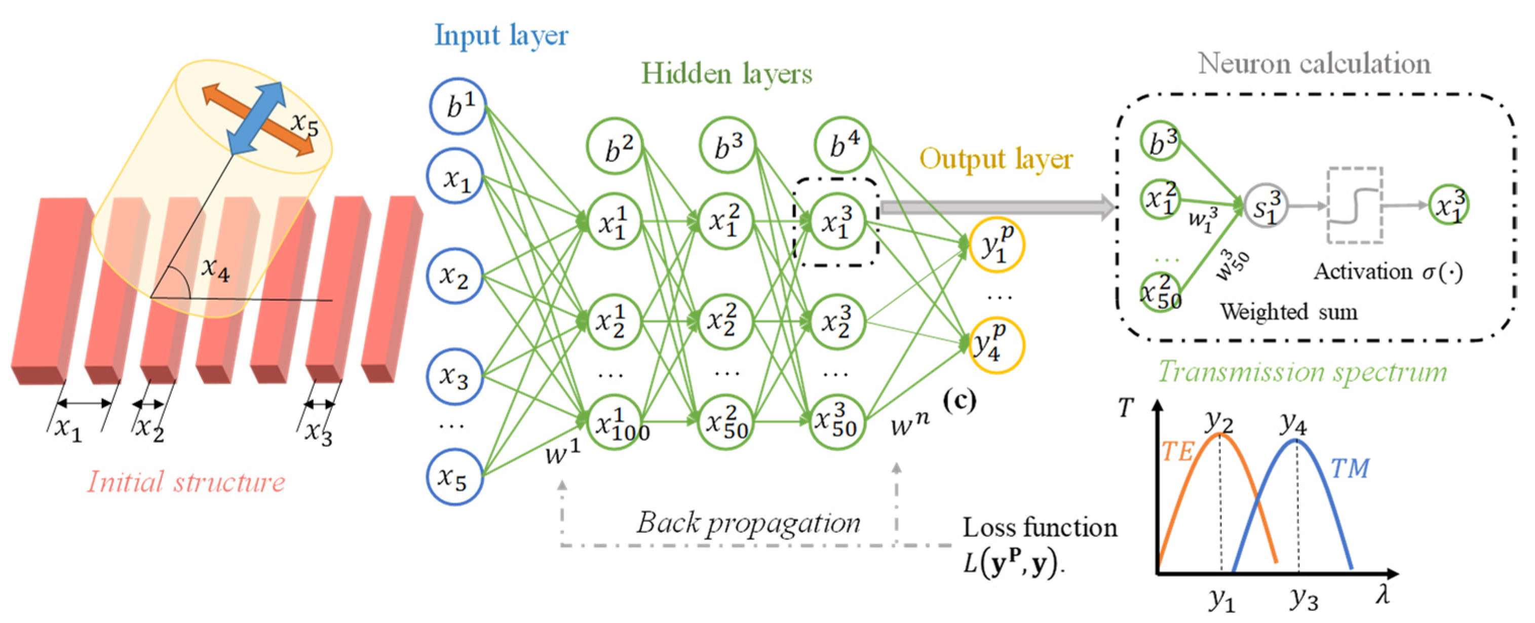
3.1.1. Multi-Layer Perceptron

The origin of MLP dates back to 1989 when Cybenko et al. proposed a feed-forward network with a single hidden layer containing a finite number of neurons. Under mild assumptions on the activation function, this neural network could approximate almost any continuous function with enough training data samples [104].
We take [85] for example to illustrate the process of constructing and training an MLP to surrogate EM simulation of grating couplers. As shown in Figure 6, the geometric parameters (grating pitch, duty cycle, fill factor, fiber angle and polarization) are encoded as data feature x = [ x 1 , x 2 , x 3 , x 4 , x 5 ] . Peak efficiencies and corresponding wavelengths for TE and TM modes are marked as data label y = [ y 1 , y 2 , y 3 , y 4 ] . The MLP adopted by Gostimirovic et al. consists of one input layer (5 neurons), three hidden layers (100, 50, 50 neurons) and one output layer (4 neurons), where the output value of each non-input neuron is determined by all the neurons in the last layer. Taking the first neuron in the third hidden layer x 1 3 for example, the weighted summation of neurons in the second hidden layer is shown in Equation (15):
s 1 3 = i = 1 50 w i 3 x i 2 + b 3 ,
where w i 3 ,   b 3 are the ith weight and bias in the third hidden layer, respectively. The weighted summation is activated to get the output value of neuron as shown in Equation (16):
x 1 3 = f ( s 1 3 ) ,
where f ( · ) is the activation function which normalizes the output of each neuron to a finite range [0, 1] or [−1, 1]. Activation functions are supposed to be computationally efficient, for there may exist abundant neurons in a DNN [105]. In this example, Rectified Linear Units (ReLu) activation function is adopted, which is expressed as in Equation (17):
f ( x ) = max ( 0 , x ) .
Through this feed-forward propagation, the relationship between input data feature x and output label y is shown in Equation (18):
y = f ( W 4 · x 3 + b 4 ) = f ( W 4 · ( W 3 · x 2 + b 3 ) + b 4 ) = = F ( x ; W , b ) ,
where W : [ W 1 , W 2 , W 3 , W 4 ] and b : [ b 1 , b 2 ,   b 3 ,   b 4 ] consists of weights and biases in all the layers. These weights and biases are determined by the training of MLP with known data samples, which is accomplished by backpropagation. Firstly, the loss function in the form of mean square error (MSE) is defined as in Equation (19):
L ( y P , y ) = 1 4 i = 1 4 ( y i p y i ) 2 ,
where y i p is the predicted value of ith output neuron and y i is the ith label of a data sample. Apart from MSE, the loss function can be expressed, e.g., in the form of cross entropy loss function [106]. The loss function L ( y p , y ) is optimized to its minimal by gradient descent, like stochastic gradient descent (SGD) or batch-size SGD. After the calculation of gradients for the tth sample, weights are updated as in Equation (20):
W ( t + 1 ) = W ( t ) + α w ( t ) L ( F ( x ( t ) ; W ( t ) ) , y ( t ) ) ,
where α is the learning rate to control the update speed. Bias b is updated in a similar way. In the example of reference [85], 9190 data samples are generated via 2D FDTD and separated with a ratio of 85:15 for training and validation. The trained MLP has 93.2% prediction accuracy and is 1830 times faster compared with FDTD simulation, hence this trained MLP is beneficial to surrogate EM simulations of grating couplers. This trained MLP is easy to connect with optimization algorithms for rapid development of new grating couplers. Gostimirovic et al. demonstrated that their trained MLP with brute-force sweeping could find an optimal design 61 times faster than FDTD simulations with PSO.
However, for increasing DOF, an MLP should be deep enough to map the data features to the data labels and the required training data samples will also increase. For example, Tahersima et al. trained an eight-layers ResNet with 20.000 data samples to predict the output spectra of power splitter with QR-code like structure [92]. Apart from increasing the layers of an MLP, reducing the dimension of data features is also an efficient way to map high-dimensional data features to the data labels, which could also alleviate the requirement for a large number of training data samples. Melati et al. have demonstrated that principal component analysis (PCA) is capable of compressing high-dimensional geometric parameters to a sub-space without useful information loss [107]. To avoid the massive data samples requirement for devices with very high DOF like irregular structures, Liu et al. adopted Fourier transform together with a high frequency filter to diminish high-frequency geometry information and then use this compressed data in Fourier domain to train an MLP as a forward model [108].

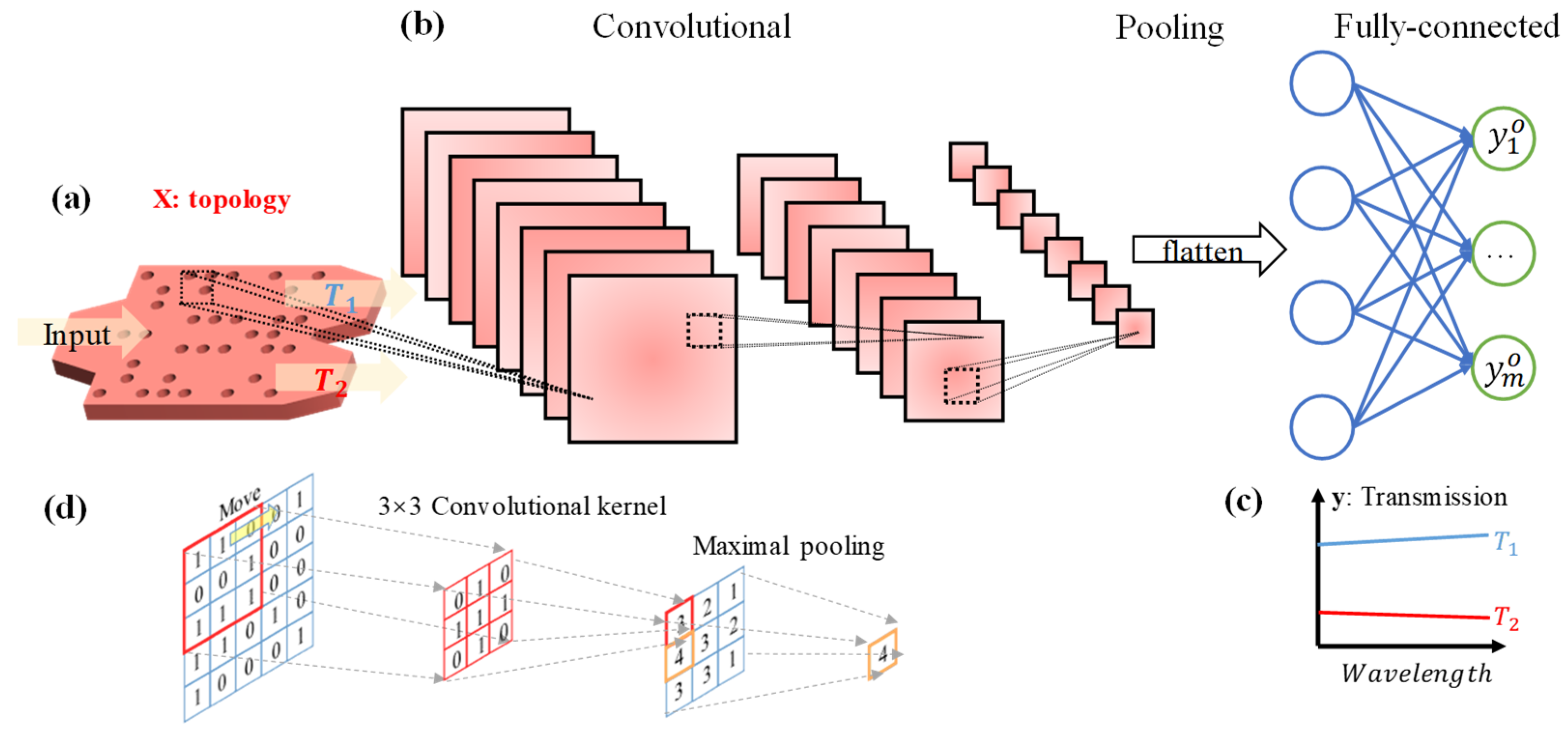
3.1.2. Convolutional Neural Network

As discussed in Section 3.1.1, MLP it is hard to process devices with high-DOF structures such as QR-code and irregular structures without introducing additional methods to reduce data dimensionality. Fortunately, CNN, another popular DNN, is innately capable of processing high-dimensional date features while requiring smaller training data samples than an MLP under the same conditions. Inspired by human visual information procedure illustrated by David (1981), CNN processes the data layer by layer from specific to abstract and has been widely used for image classification, separation and recognition [109]. A complete CNN usually consists of three types of layers, i.e., convolutional layers, pooling layers and fully-connected layers. Convolutional layers extract local features of an input data matrix, while pooling layers, also called down-sampling layers, reduce the data dimensionalities greatly and avoid overfitting. The fully-connected layers are similar to an MLP, which project extracted data features to the data labels.
We take reference [86] as an example to illustrate the process of building and training a CNN as a forward model to predict output spectra of a QR-code like power splitter. As shown in Figure 7a, this power splitter consists of one inverse tapered input waveguide, two tapered output waveguides and a 2.6 × 2.6 μm2 middle square design area which is separated into 20 × 20 pixels. Each of these pixels has a binary state as etched (coded as 1) with a diameter of 90 nm circle and not-etched (coded as 0). This 0–1 coded 20 × 20 matrix works as the input data features X of CNN, which goes through three convolutional layers with ReLu activation. In a convolutional layer, different convolutional kernels convolve with input matrix to generate different sub-matrices as shown in Figure 7b. After convolutional layers, the extracted features are condensed via pooling layers and flattened into a vector. This vector containing extracted features is then projected to data labels y via fully-connected layers with Sigmoid activation function. The data labels are vectors with samples of transmission spectra as their elements shown in Figure 7c. After the training, this CNN predicted transmission performance with 85% accuracy compared with simulation results, which was much better than 16% accuracy of a 4-layered MLP using the same training data samples. Thus, a well-trained CNN is preferred for predicting the optical performance of devices with QR-code structures.
A simple example of convolutional and maximal pooling processes is demonstrated in Figure 7d. As shown in the red square, the pre-defined convolutional kernel is multiplexed to pixels in the original matrix to get a new value in sub-matrix. Moving the convolutional kernel along the original 5 × 5 matrix, we get a 3 × 3 sub-matrix. To further decrease the matrix dimension, maximal pooling operation is performed, where only the maximum value is picked up to represent the sub-matrix as marked by orange squares. These convolutional and pooling layers are widely used for high-dimensional image data processing and are easy to train.

3.2. Training Generative Deep Neural Networks as Inverse Models

A well-trained inverse model can predict the component geometries directly according to target optical responses without any iterative optimization procedures. However, it is difficult to build and train a DNN as an inverse model because a specific optical response corresponds to different component geometries, which is hard to model via discriminative neural networks. Luckily, generative neural networks can solve this one-to-many projection [110]. Instead of fitting data features to data labels directly, generative neural networks model the underlying distributions of data features x (device geometry parameters) and data labels y (optical response). However, training of generative neural networks is hard to converge without enough data samples. To ease the burden of massive requirement of training data samples, semi-supervised generative neural networks like conditional variational autoencoder (CVAE) and conditional generative adversarial network (CGAN) have been proposed for building inverse models [91,103,111]. Furthermore, combined with an EM simulator such as FDTD, unsupervised generative neural networks have also been trained as inverse models, where prepared training data samples are not demanded [99,100].

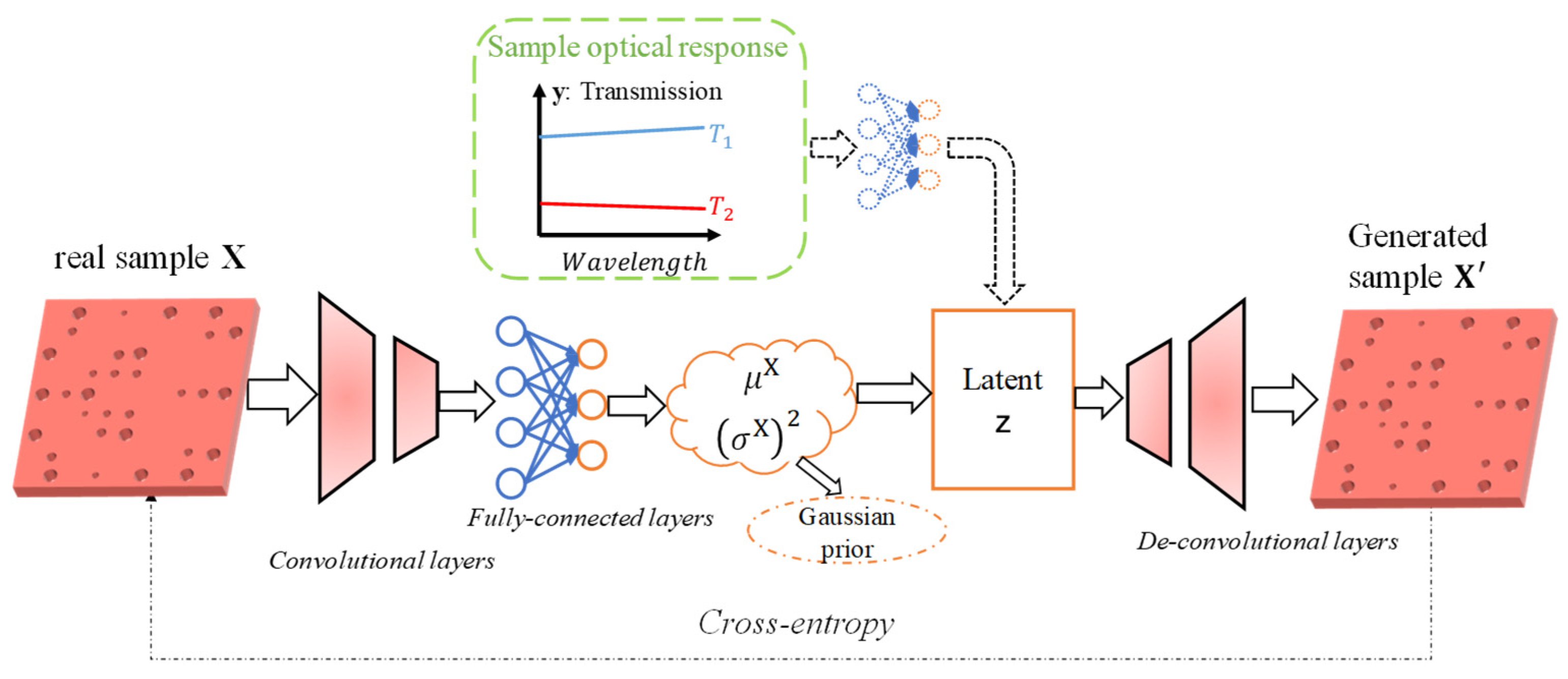
3.2.1. Conditional Variational Autoencoder

Variational autoencoder (VAE), a kind of generative neural network, generates data features through a decoder with sampled normal distribution input [112]. The input of a decoder is supposed to have the same normal distributions with the output of an encoder. In the training process, an encoder projects original data features to their unique mean values and variances, which are supposed to obey normal distributions, while a decoder tries to reconstruct original data features through potential variables sampled from normal distributions. The VAE is trained by minimizing the difference between real features from data samples and generated features from VAE and by ensuring that the encoded data obeys normal distributions. After the training process, different groups of new data features can be generated by sampling different potential variables from the normal distributions and feeding them into encoder. However, VAE can only generate data features (e.g., device geometry) similar to their training data samples, which is not suitable for an inverse design problem where a data label (target optical response) is desired. Fortunately, CVAE is a kind of model which melts label information into a VAE so that the trained model could generate data features according to data labels.
We take reference [91] as an example to illustrate how to train a CVAE as an inverse model to generate component geometry according to user-defined optical spectrum. The initial power splitter structure is similar to the structure in Figure 7 with 20 × 20 pixels in the middle square design area but the diameters of etched holes are tunable to increase the DOF of QR-code structure. 20 × 20 data features X with values ranging from 0 to 1 are used to represent these holes, where the variables with value less than 0.3 represent no hole and variables with value [0.3~1] correspond to etched holes with diameters [44~77 nm]. As shown in Figure 8, features X from real data samples are encoded through convolutional layers and fully-connected layers into mean values μ and variances σ . The latent vector z which are sampled from Gaussian distributions described by μ and σ are concatenated with coded optical response y to work as the input of autoencoder. After two de-convolutional layers and pooling layers, a geometry similar with training data samples is generated. The aim of the training process is to diminish the difference between original and generated geometric parameters and to decrease the Kullback-Leibler (KL) divergence between the latent z and the Gaussian prior. Prepared 15,000 training data samples, including some semi-optimized power splitters with different splitting ratios, are used to train this CVAE. The trained CVAE then generates 1000 new geometrical patterns according to different splitting ratios within seconds, which are validated by FDTD and marked with labels to train the CVAE again for better performance. This trained CVAE is able to generate power splitters with 90% efficiencies for given splitting ratios.

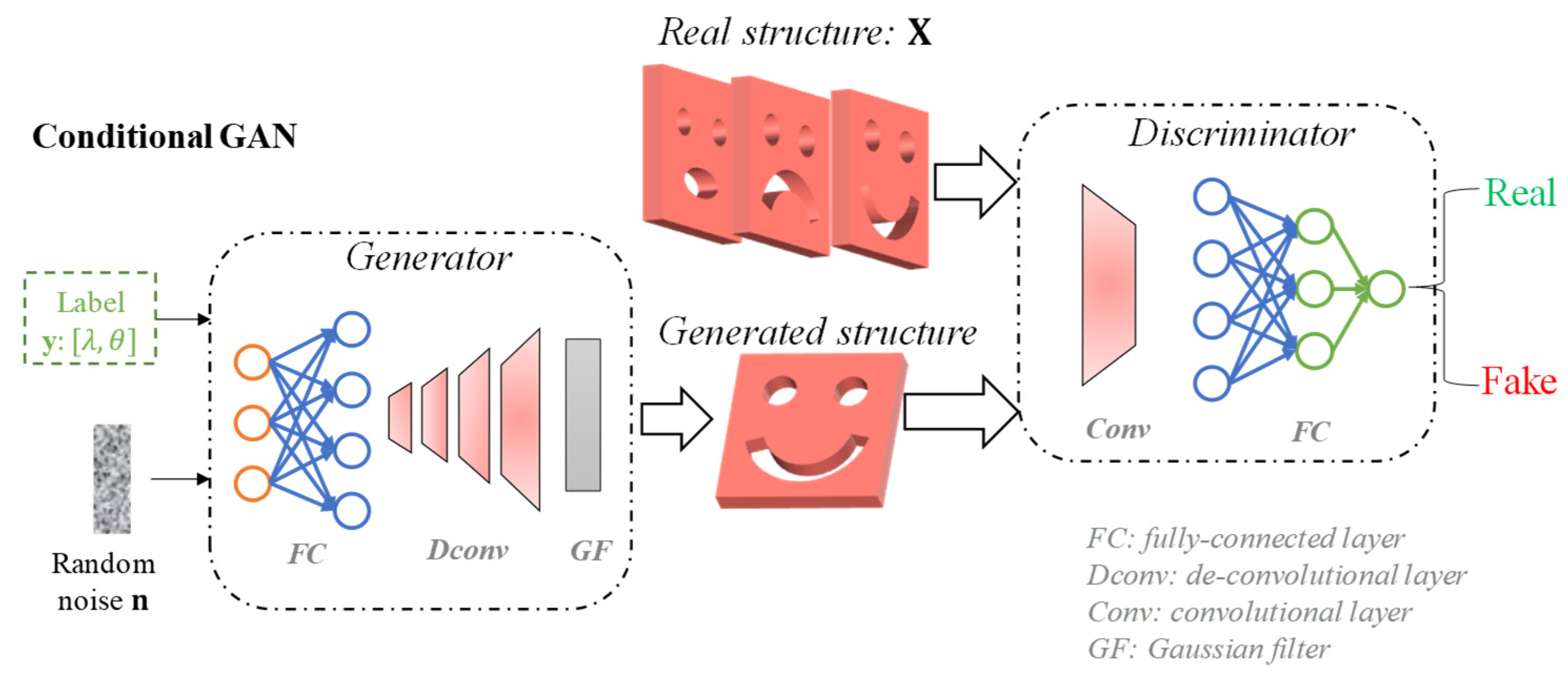
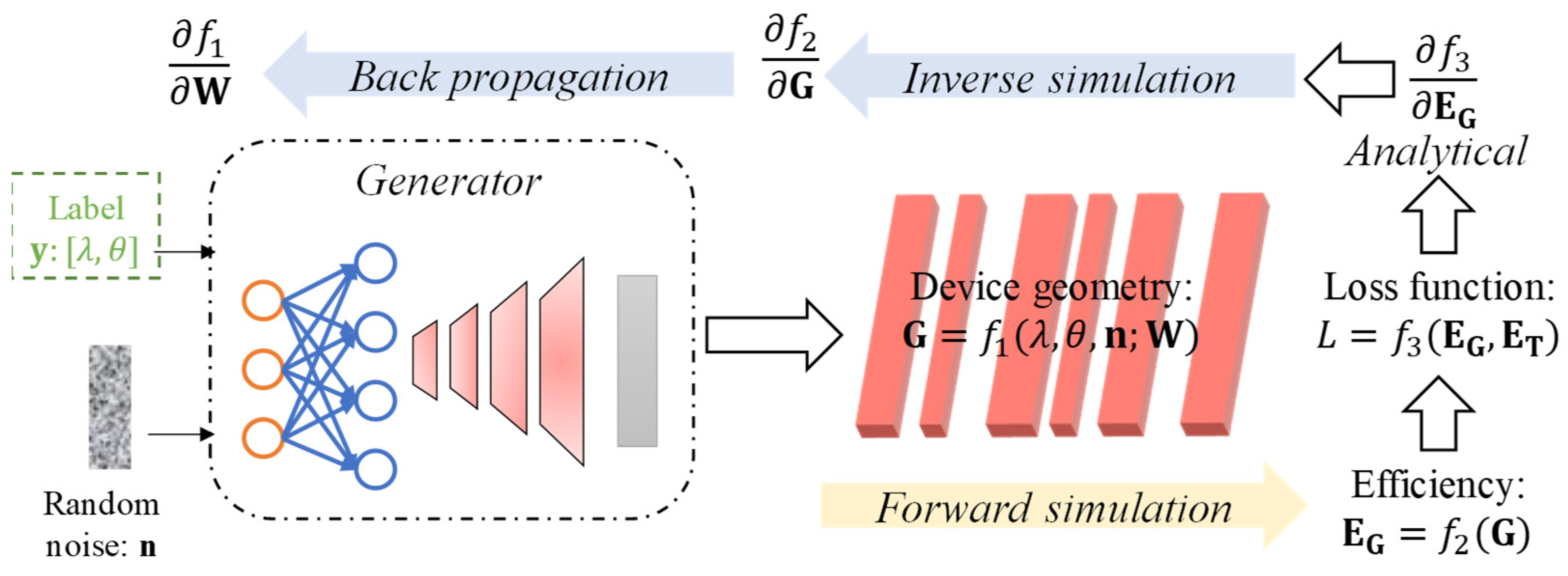
3.2.2. Conditional Generative Adversarial Network

Different from VAE which encodes original data features into normal distributions and decodes these normal distributions to reconstruct original data features, a generative adversarial network (GAN) uses a kind of game theory for training [113]. A GAN consists of a generator and a discriminator which compete with each other. With random noise input, generator produces a group of generated data features (e.g., device geometry parameters) while the discriminator judges whether this group of generated data features is real or not. The training of GAN is a game process where the generator intends to fool discriminator with generated data features and the discriminator tries to distinguish generated features from the original ones. Firstly, the discriminator is trained several times to distinguish generated features from original features. Then, the discriminator works as a supervisor to train the generator until the generator can produce data features to deceive the discriminator itself. The training procedures of discriminator and generator are alternatively repeated several times until the generator can produce almost “real” data features. Like a CVAE, a CGAN also merges data labels into the model to generate new data features. Random noise and data labels are concatenated and then applied as input to the generator.
We take reference [103] as an example to illustrate the process of training a CGAN as an inverse model to predict the irregular geometries of metagratings. The target optical properties are diffraction angle θ and diffraction wavelength λ . As shown in Figure 9, the label y which describes the optical properties is combined with random noise to work as the input of generator. The random noise n is utilized to improve the robustness of the generator as well as to generate different irregular geometries. The generator, which consists of two fully-connected layers, four de-convolutional layers and a Gaussian filter, produces new irregular geometries. The discriminator consists of convolutional layers and fully-connected layers. It works as a supervisor to determine whether a generated irregular geometry shares the same properties with the prepared irregular geometries. The generator and discriminator are trained alternately. 600 high-resolution irregular half-optimized metagratings are used as the initial training data samples. After training, the CGAN generates thousands of irregular metagratings within seconds. They are used as new training data samples to retrain CGAN for better performance. Most of the generated metagratings from the trained CGAN have efficiencies over 75%, much better than randomly generated metagratings whose best efficiency is less than 30%. The efficiency of irregular metagratings generated by CGAN together with a few iterative optimization procedures could reach up to over 90%, comparable to that of iterative-only optimization methods.
Using a CGAN, Liu et al. further merged a pre-trained forward neural network with CGAN to calculate the optical response of a generated device [114]. The generator was trained with two aims: the first to diminish the difference between generated structure and real structures under the supervision of discriminator, and the second to reduce the difference between targeted optical response and generated optical response which is calculated via pre-trained forward neural network. In this way, apart from making the generated device geometry similar to real device structures, the transmission efficiency of generated device is also supposed to be similar to the target optical response.

3.2.3. Unsupervised Generative Neural Network

In addition to learning from the data samples, DNN can also work as a trainable function and merge with EM-simulator based optimization algorithms. In this way, training data samples are not required.
We take reference [100] as an example to illustrate the process of building and training an unsupervised neural network as an inverse model to generate irregular metagratings. The irregular geometries of metagrating are also produced by a well-trained generator for the given optical response as well as random noise. As shown in Figure 10, the device geometry G is the function of diffraction wavelength λ , angle θ and random noise n as shown in Equation (21):
G = f 1 ( λ , θ , n ; W ) ,
where f 1 ( · ) is the function described by the generator with trainable parameters matrix W . With known metagrating geometry G , the optical response E G can be calculated by forward EM simulation as in Equation (22):
E G = f 2 ( G ) ,
where f 2 ( · ) is the non-analytical function computed by EM simulation. The loss function is an analytical function defined by designer as in Equation (23):
L = f 3 ( E T ,   E G ) .
The aim of f 3 ( · ) is to diminish the difference between target optical response E T and generated optical response E G . To train this deep generator, back-propagation is applied as in Equation (24):
L W = L E G · E G G · G W = f 3 E G · f 2 G · f 1 W .
The first term f 3 E G is an explicit function, which is easy to calculate analytically. The second term f 2 G , which is an implicit function, can be solved through adjoint method with an inverse simulation as derived in Section 2. The last term f 1 W , is the loss function of deep generator which can be trained via back-propagation similar to other DNNs.
In this way, the generator is no longer trained by prepared data samples but with the assistance of EM simulation in a chain rule. After the training process, the generator is able to produce multiple metagratings with different geometric parameter sets for a target optical response.
Reinforcement learning which merges DNN with EM simulator is another approach without the need of training data samples. DNNs based on reinforcement learning generate new data features which are evaluated by EM simulator and fed back for the training of DNNs. Sajedian et al. utilized reinforcement learning for silicon-based color printing design [101]. Different from examples discussed above which make use of gradient of EM simulator, reinforcement learning makes decisions on the rewards of short-term and long-term gains.

3.3. Comparision of DNNs for the Design of Nanophotonics on Silicon Platform

In this section, we discussed some popular DNNs used as forward models and inverse models to accelerate the design process of silicon photonics. Here, we will classify and compare the advantages and disadvantages of these DNNs for the design of nanophotonics on silicon platform.
Forward model built via DNN serves as a boosted EM simulator for devices with similar initial structures to the training data samples. A well-trained forward model can predict optical response for given geometric parameters at almost no time cost. Combining forward model with iterative optimization algorithms, geometric parameters for a target optical response can be quickly optimized. MLP and CNN are both discriminative neural networks and have been widely used for the forward models. MLP is the simplest and most efficient DNN for geometries with low DOF such as empirical structures. With increasing DOF, both the number of training data samples and the depth of MLP structure have to be increased greatly. Data dimensionality reduction approaches can also be used to map high-DOF devices to low data dimension, but tricky data preprocessing is needed in that case. Another method is to merge data preprocessing directly into DNNs like CNN, whose convolutional layers and pooling layers are innately capable of processing high-dimensional data features. CNN is widely used for components with QR-code like structure or irregular structure.
Inverse models are more attractive for that they generate component geometry parameters for a target optical response almost without iterative optimization processes involved. However, an inverse model is much more difficult to build and train. Firstly, one optical response corresponds to not only one group of geometric parameters. Secondly, optical response usually has lower dimensionality as compared to geometry parameters. Luckily, generative neural networks such as CVAE and CGAN are capable of projecting low dimension to high dimension. Both of them try to monitor the underlying distributions of geometric parameters and optical response. The difference is that CVAE gets the underlying distribution via encoder and CGAN utilizes a discriminator to judge whether generated geometric parameters share the same distribution with data samples. This structural difference also brings training difference: CVAE trains the encoder and decoder simultaneously while CGAN trains two DNNs as generator and discriminator in an alternate way. After training, with optical response and potential variables as input, a CVAE generates device geometric parameters via a decoder while a CGAN produces geometric parameters via a generator.
Inverse models based on unsupervised generative neural networks are also appealing because they do not require training data samples. However, the time-consuming EM simulator has to be inserted into the generative neural networks to guarantee that they obey physical laws. Once trained, unsupervised generative neural networks can also generate new geometric parameters according to target optical response without any simulator involved.

4. Prospective

As discussed above, both iterative optimization algorithms and DNNs play vital roles in the inverse design of compact and high-performance silicon photonics. However, there are also some problems for these design methodologies. In this section, we will discuss the challenges of existing design methodologies and future research directions of inverse design in silicon photonics.

4.1. Challenges of Existing Optimization Methodologies

4.1.1. Simulation Time Budget

Gradient-free algorithms such as heuristic algorithms and DBS are widely used in inverse design. However, these methods require a great number of EM simulations to find the parameters set for an acceptable FOM. Heuristic algorithms need to perform EM simulations several times the DOF at each iteration to find the parameters update directions. DBS as a brute-force searching scheme is mainly used for devices with QR-code structures. Each simulation will only update one pixel, thus the required number of simulations to update the whole QR code during one round is the same as DOF. Usually, several rounds of DBS are needed for a device to reach an acceptable FOM. Chen et al. have shown that it takes more than 5000 simulations to optimize a mode convertor with 1120 DOF [115]. With increasing DOF of devices, the time budget of required simulations will be extremely large. Therefore, they proposed a new method which combined DBS with gradient-based algorithms. In this way, the total number of simulations could be cut down at the cost of some decrease in performance. Improving the efficiency of gradient-free algorithms is a prerequisite for further applying them to the design of more complicated devices.
In addition to cutting down the number of EM simulations required for the iterative optimization, a time-efficient EM simulator can also reduce the time budget for inverse design. Even though 3D-FDTD is computationally intensive, the simulation speed scales with multiple processors. High-performance computing techniques including parallelization and distributed computing are already adopted for commercial [116] and open-source [117] FDTD solvers, allowing the designers to reduce simulation time by additional computing resources. Implementation of FDTD or FEM using graphics processing unit (GPU) has also been investigated for higher simulation speed [118,119]. Advances in these attempts will also help reduce the time budget for inverse design.

4.1.2. Local Optimum and Minimal Features

TO is capable of optimizing the free-form irregular devices with thousands of DOF. However, inappropriate initial structures may limit the final optical performance to a local optimal. It takes trials and errors before finding an appropriate initial structure for a specific target. This issue could be solved by designing initial structure according to the physical laws or automatically adjusting initial structures based on optimization results. More interestingly, some researchers combine topology optimization with DNNs for global optimization for silicon metagratings [100], which could also be introduced to the design of integrated silicon photonics.
Another emerging problem for free-form TO is that the optimized devices may have very small features which could be difficult for fabrication process. Apart from “soft” control methods such as filter-based or transform domain-based methods, “hard” control methods have also been proposed. For example, Wang et al. confined the device structure to be QR-code with controllable minimal feature size [120]. However, these “digital” devices constrain the minimal feature size at the cost of DOF. More efficient methods to avoid local optimum and control minimal feature size are still desired for gradient-based freeform optimizations.

4.1.3. Data Sample Issue

Training a fully supervised DNN as a forward model takes around 10,000 data samples, as examples in Section 3.2 suggested. These data samples are collected by time-consuming EM simulations, which may cost even more time than iterative optimization algorithms. Therefore, DNNs-based forward models could only show their advantages in scenarios where piles of similar devices are needed. Data dimensionality reduction methods like PCA and Fourier transform have been applied to ease the burden of data samples collection but the effect is not satisfactory. For PCA, optimized data samples are required to find the lower-dimensional sub-space. For Fourier transform, some information will be discarded by high-frequency filters.
Inverse models project low-dimensional data labels to high-dimensional data features, which require even more data samples compared to forward model using traditional DNNs. The number of data samples can be reduced to a few thousand or hundreds by using semi-supervised DNNs, such as CVAE or CGAN. However, these inverse models require optimized or semi-optimized data samples. Without high-performance training data samples, the generative neural networks are hard to generate devices with high optical performance. Lowering the demand on the number and quality of training data samples is a good direction for future research. Unsupervised learning for inverse models totally solves the problems of massive data samples collection. However, an EM-simulator must merge into the training process of unsupervised generative neural networks to guarantee that the unsupervised DNN obeys physical rules. Apart from the time-consuming training process where EM-simulator has to be involved, inverse models based on unsupervised DNNs are not as general as those based on supervised DNNs. In other words, a well-trained DNN with the help of an EM-simulator may not be suitable for devices with diverse optical properties because such DNN is trained towards the direction of a target optical response. Improving the versatility of unsupervised-learning-based inverse models is also an interesting and meaningful topic for further study.

4.2. Application of Inverse Design in Optical Neural Networks

Artificial intelligence, which mimics the human learning process, is capable of processing many problems in almost every field. With the increasing demands of higher computational resources for complex tasks, traditional electronics-based computation is reaching its limits. ONN is an appealing alternative to conventional electronic computation for handling complex tasks since optics can process parallel computations with much lower power consumption [3,12,121,122,123]. There are two popular integrated ONN schemes. i.e., layered ONNs and “black-box” ONNs.

4.2.1. Layered ONNs

Layered ONNs mimic traditional layered feed-forward neural networks, which consist of convolutional layers or fully-connected layers. Taking fully-connected layers for example, the weights matrix W can be decomposed by singular value decomposition (SVD) as W = U Σ V T , where U and V T are the unitary matrices and Σ is the diagonal matrix. It has been proved that the unitary matrix could be realized via all-optical devices [124,125] and the diagonal matrix could be achieved by attenuators. Shen et al. cascaded programmable Mach-Zehnder interferometers (MZI) for different unitary matrix designs [126], while Qu et al. utilized topology optimization algorithm to design the unitary matrix, which is much more compact than cascaded MZI [80]. In both of the above-mentioned ONN architectures, the optical weights matrices are connected to a personal computer for realizing nonlinear activation, as optics are linear in silicon platform when the intensity of input light is low. In fact, the computation speed of a trained ONN is several orders faster than the traditional electronic DNNs with comparable prediction accuracy. With optical activation function, the computation speed could be accelerated even more [127]. Inverse design of nonlinear material proposed by Hughes et al. can be used for designing such optical activation function [128]. Similarly, Chen et al. utilized phase change material (PCM) inserted in silicon platform to work as an optical switch [129] which can also be inserted into silicon platform for activation function design.

4.2.2. “Black-Box” ONNs

“Black-box” ONNs go beyond the paradigm of layered feed-forward networks. Through an inverse designed platform, “black-box” ONNs map input signal to desired output ports directly. For example, Khoram et al. utilized the nanophotonic neural medium (NNM) to realize handwritten digital recognition [130]. The handwritten digits are modulated to optical signals and fed to the input waveguides of NNM. After interactions with NNM, the modulated optical signals are transferred to ten output waveguides, which represent digits from 0 to 9. The output waveguide ports with highest light intensity suggests the input digit to be such value. Their “black-box” ONN is shown to be much more compact than the layered ONNs as no layers or neurons are needed in this case. However, the “black-box” ONN is not scalable. For more difficult tasks, the footprint of “black-box” ONN needs to be increased, which makes the inverse design of NNM too time-consuming to be realized.
Integrating all optical neural networks on silicon platform is still an emerging and significant research topic. The silicon platform with large effective refractive index is compatible to CMOS technology, which makes the cheap and massive fabrication possible. With the assistance of inverse design, many compact components could be designed and integrated for complex ONNs, while energy consumption can be reduced comparing with electronic DNNs.

5. Conclusions

Silicon photonics has been widely researched due to its high refractive index, where light could be manipulated efficiently even in the subwavelength scale. Different inverse design methods have been proposed and improved to reach the design limit of silicon platform for different application scenarios with high computation efficiency. In this review paper, we summarized the iterative optimization methods as well as newly-proposed DNNs for the inverse design of silicon photonics. For iterative optimization methods, we introduced heuristic algorithms like GA, PSO, DBS and TO for different scenarios in the sequence of increased DOF. DNNs-assisted inverse design could generate multiple devices with similar design area and optical response several orders of times faster than iterative optimization algorithms, which is particularly useful for situations like arbitrary power splitters where many optical devices are needed. In addition, we highlighted open issues with existing inverse design methodologies such as the great time budget for gradient-free algorithms, the local optimum of gradient-based algorithms and the data burden of DNNs. Since ONNs are quite appealing with the growing demand of artificial intelligence in various fields, we also discussed the role of inverse design and its corresponding methodologies for realizing ONNs. Inverse-designed ONN would be an interesting topic for future research in silicon photonics.

Author Contributions

Conceptualization, all authors; investigation, S.M. and L.C.; original draft preparation, S.M.; review and editing, all authors; supervision, H.Y.F. and F.N.K.; funding acquisition, H.Y.F. All authors have read and agreed to the published version of the manuscript.

Funding

This research was funded by the Shenzhen Science and Technology Innovation Commission (Projects: JCYJ20180507183815699), Guangdong Basic and Applied Basic Research Foundation (2021A1515011450) and Tsinghua-Berkeley Shenzhen Institute (TBSI) Faculty Start-up Fund.

Institutional Review Board Statement

Not applicable.

Informed Consent Statement

Not applicable.

Data Availability Statement

Not applicable.

Conflicts of Interest

The authors declare no conflict of interest.

References

  1. Jalali, B.; Fathpour, S. Silicon Photonics. J. Lightwave Technol. 2006, 24, 4600–4615. [Google Scholar] [CrossRef]
  2. Thomson, D.; Zilkie, A.; Bowers, J.E.; Komljenovic, T.; Reed, G.T.; Vivien, L.; Marris-Morini, D.; Cassan, E.; Virot, L.; Fédéli, J.-M.; et al. Roadmap on silicon photonics. J. Opt. 2016, 18. [Google Scholar] [CrossRef]
  3. Ferreira de Lima, T.; Shastri, B.J.; Tait, A.N.; Nahmias, M.A.; Prucnal, P.R. Progress in neuromorphic photonics. Nanophotonics 2017, 6, 577–599. [Google Scholar] [CrossRef]
  4. Hu, T.; Dong, B.; Luo, X.; Liow, T.-Y.; Song, J.; Lee, C.; Lo, G.-Q. Silicon photonic platforms for mid-infrared applications [Invited]. Photonics Res. 2017, 5. [Google Scholar] [CrossRef] [Green Version]
  5. Xie, W.; Komljenovic, T.; Huang, J.; Tran, M.; Davenport, M.; Torres, A.; Pintus, P.; Bowers, J. Heterogeneous silicon photonics sensing for autonomous cars. Opt. Express 2019, 27, 3642–3663. [Google Scholar] [CrossRef]
  6. Jiang, J.; Chen, M.; Fan, J.A. Deep neural networks for the evaluation and design of photonic devices. Nat. Rev. Mater. 2020. [Google Scholar] [CrossRef]
  7. Molesky, S.; Lin, Z.; Piggott, A.Y.; Jin, W.; Vucković, J.; Rodriguez, A.W. Inverse design in nanophotonics. Nat. Photonics 2018, 12, 659–670. [Google Scholar] [CrossRef] [Green Version]
  8. So, S.; Badloe, T.; Noh, J.; Bravo-Abad, J.; Rho, J. Deep learning enabled inverse design in nanophotonics. Nanophotonics 2020, 9, 1041–1057. [Google Scholar] [CrossRef] [Green Version]
  9. Li, W.; Meng, F.; Chen, Y.; Li, Y.f.; Huang, X. Topology Optimization of Photonic and Phononic Crystals and Metamaterials: A Review. Adv. Theory Simul. 2019, 2. [Google Scholar] [CrossRef]
  10. Elsawy, M.M.R.; Lanteri, S.; Duvigneau, R.; Fan, J.A.; Genevet, P. Numerical Optimization Methods for Metasurfaces. Laser Photonics Rev. 2020, 14. [Google Scholar] [CrossRef]
  11. Hegde, R.S. Deep learning: A new tool for photonic nanostructure design. Nanoscale Adv. 2020, 2, 1007–1023. [Google Scholar] [CrossRef]
  12. Yao, K.; Unni, R.; Zheng, Y. Intelligent nanophotonics: Merging photonics and artificial intelligence at the nanoscale. Nanophotonics 2019, 8, 339–366. [Google Scholar] [CrossRef]
  13. Paz, A.; Moran, S. Non deterministic polynomial optimization problems and their approximations. Theor. Comput. Sci. 1981, 15, 251–277. [Google Scholar] [CrossRef] [Green Version]
  14. Ma, L.; Li, J.; Liu, Z.; Zhang, Y.; Zhang, N.; Zheng, S.; Lu, C. Intelligent algorithms: New avenues for designing nanophotonic devices. Chin. Opt. Lett. 2021, 19, 011301. [Google Scholar]
  15. Jensen, J.S.; Sigmund, O. Topology optimization for nano-photonics. Laser Photonics Rev. 2011, 5, 308–321. [Google Scholar] [CrossRef]
  16. Tu, X.; Xie, W.; Chen, Z.; Ge, M.-F.; Huang, T.; Song, C.; Fu, H.Y. Analysis of Deep Neural Network Models for Inverse Design of Silicon Photonic Grating Coupler. J. Lightwave Technol. 2021. [Google Scholar] [CrossRef]
  17. Otto, A.; Marais, N.; Lezar, E.; Davidson, D. Using the FEniCS package for FEM solutions in electromagnetics. IEEE Antennas Propag. Mag. 2012, 54, 206–223. [Google Scholar] [CrossRef]
  18. Gedney, S.D. Introduction to the finite-difference time-domain (FDTD) method for electromagnetics. Synth. Lect. Comput. Electromagn. 2011, 6, 1–250. [Google Scholar] [CrossRef]
  19. Bienstman, P. Rigorous and efficient modelling of wavelenght scale photonic components. Ph.D. Thesis, Ghent University, Ghent, Belgium, 2001. [Google Scholar]
  20. Moharam, M.; Grann, E.B.; Pommet, D.A.; Gaylord, T. Formulation for stable and efficient implementation of the rigorous coupled-wave analysis of binary gratings. JOSA a 1995, 12, 1068–1076. [Google Scholar] [CrossRef]
  21. Luo, L.W.; Ophir, N.; Chen, C.P.; Gabrielli, L.H.; Poitras, C.B.; Bergmen, K.; Lipson, M. WDM-compatible mode-division multiplexing on a silicon chip. Nat. Commun 2014, 5, 3069. [Google Scholar] [CrossRef] [Green Version]
  22. Guan, H.; Ma, Y.; Shi, R.; Novack, A.; Tao, J.; Fang, Q.; Lim, A.E.; Lo, G.Q.; Baehr-Jones, T.; Hochberg, M. Ultracompact silicon-on-insulator polarization rotator for polarization-diversified circuits. Opt. Lett. 2014, 39, 4703–4706. [Google Scholar] [CrossRef]
  23. Wang, Q.; Ho, S.T. Ultracompact Multimode Interference Coupler Designed by Parallel Particle Swarm Optimization With Parallel Finite-Difference Time-Domain. J. Lightwave Technol. 2010, 28, 1298–1304. [Google Scholar] [CrossRef]
  24. Chen, W.; Zhang, B.; Wang, P.; Dai, S.; Liang, W.; Li, H.; Fu, Q.; Li, J.; Li, Y.; Dai, T.; et al. Ultra-compact and low-loss silicon polarization beam splitter using a particle-swarm-optimized counter-tapered coupler. Opt. Express 2020, 28, 30701–30709. [Google Scholar] [CrossRef]
  25. Mao, S.; Cheng, L.; Mu, X.; Wu, S.; Fu, H. Ultra-Broadband Compact Polarization Beam Splitter Based on Asymmetric Etched Directional Coupler. In Proceedings of the Conference on Lasers and Electro-Optics/Pacific Rim, Sydney, Australia, 3 August 2020; p. C12H_11. [Google Scholar]
  26. Zhu, L.; Sun, J. Silicon-based wavelength division multiplexer by exploiting mode conversion in asymmetric directional couplers. OSA Contin. 2018, 1. [Google Scholar] [CrossRef]
  27. Bogaerts, W.; De Heyn, P.; Van Vaerenbergh, T.; De Vos, K.; Kumar Selvaraja, S.; Claes, T.; Dumon, P.; Bienstman, P.; Van Thourhout, D.; Baets, R. Silicon microring resonators. Laser Photonics Rev. 2012, 6, 47–73. [Google Scholar] [CrossRef]
  28. Fu, P.-H.; Huang, T.-Y.; Fan, K.-W.; Huang, D.-W. Optimization for Ultrabroadband Polarization Beam Splitters Using a Genetic Algorithm. IEEE Photonics J. 2019, 11, 1–11. [Google Scholar] [CrossRef]
  29. Dai, D.; Bowers, J.E. Novel ultra-short and ultra-broadband polarization beam splitter based on a bent directional coupler. Opt. Express 2011, 19, 18614–18620. [Google Scholar] [CrossRef] [PubMed]
  30. AlTaha, M.W.; Jayatilleka, H.; Lu, Z.; Chung, J.F.; Celo, D.; Goodwill, D.; Bernier, E.; Mirabbasi, S.; Chrostowski, L.; Shekhar, S. Monitoring and automatic tuning and stabilization of a 2 × 2 MZI optical switch for large-scale WDM switch networks. Opt. Express 2019, 27, 24747–24764. [Google Scholar] [CrossRef] [PubMed]
  31. Mao, S.; Cheng, L.; Wu, S.; Mu, X.; Tu, X.; Li, Q.; Fu, H. Compact Five-mode De-multiplexer based on Grating Assisted Asymmetric Directional Couplers. In Proceedings of the Asia Communications and Photonics Conference, Beijing, China, 24–27 October 2020; p. M4A-128. [Google Scholar]
  32. Wu, S.; Mao, S.; Zhou, L.; Liu, L.; Chen, Y.; Mu, X.; Cheng, L.; Chen, Z.; Tu, X.; Fu, H.Y. A compact and polarization-insensitive silicon waveguide crossing based on subwavelength grating MMI couplers. Opt. Express 2020, 28, 27268–27276. [Google Scholar] [CrossRef]
  33. Majumder, A.; Shen, B.; Polson, R.; Menon, R. Ultra-compact polarization rotation in integrated silicon photonics using digital metamaterials. Opt. Express 2017, 25, 19721–19731. [Google Scholar] [CrossRef]
  34. Chang, W.; Lu, L.; Ren, X.; Li, D.; Pan, Z.; Cheng, M.; Liu, D.; Zhang, M. Ultra-compact mode (de) multiplexer based on subwavelength asymmetric Y-junction. Opt. Express 2018, 26, 8162–8170. [Google Scholar] [CrossRef]
  35. Xu, P.; Zhang, Y.; Zhang, S.; Chen, Y.; Yu, S. Scaling and cascading compact metamaterial photonic waveguide filter blocks. Opt. Lett. 2020, 45, 4072–4075. [Google Scholar] [CrossRef] [PubMed]
  36. Lu, C.; Liu, Z.; Wu, Y.; Xiao, Z.; Yu, D.; Zhang, H.; Wang, C.; Hu, X.; Liu, Y.C.; Liu, X.; et al. Nanophotonic Polarization Routers Based on an Intelligent Algorithm. Adv. Opt. Mater. 2020, 8. [Google Scholar] [CrossRef]
  37. Shen, B.; Polson, R.; Menon, R. Metamaterial-waveguide bends with effective bend radius < λ0/2. Opt. Lett. 2015, 40, 5750–5753. [Google Scholar] [CrossRef] [PubMed]
  38. Lu, L.; Liu, D.; Zhou, F.; Li, D.; Cheng, M.; Deng, L.; Fu, S.; Xia, J.; Zhang, M. Inverse-designed single-step-etched colorless 3 dB couplers based on RIE-lag-insensitive PhC-like subwavelength structures. Opt. Lett. 2016, 41, 5051–5054. [Google Scholar] [CrossRef]
  39. Jia, H.; Zhou, T.; Fu, X.; Ding, J.; Yang, L. Inverse-Design and Demonstration of Ultracompact Silicon Meta-Structure Mode Exchange Device. ACS Photonics 2018, 5, 1833–1838. [Google Scholar] [CrossRef]
  40. Shen, B.; Wang, P.; Polson, R.; Menon, R. An integrated-nanophotonics polarization beamsplitter with 2.4 × 2.4 μm2 footprint. Nat. Photonics 2015, 9, 378–382. [Google Scholar] [CrossRef]
  41. Xu, K.; Liu, L.; Wen, X.; Sun, W.; Zhang, N.; Yi, N.; Sun, S.; Xiao, S.; Song, Q. Integrated photonic power divider with arbitrary power ratios. Opt. Lett. 2017, 42, 855–858. [Google Scholar] [CrossRef] [Green Version]
  42. Liu, Z.; Liu, X.; Xiao, Z.; Lu, C.; Wang, H.-Q.; Wu, Y.; Hu, X.; Liu, Y.-C.; Zhang, H.; Zhang, X. Integrated nanophotonic wavelength router based on an intelligent algorithm. Optica 2019, 6. [Google Scholar] [CrossRef]
  43. Shen, B.; Polson, R.; Menon, R. Integrated digital metamaterials enables ultra-compact optical diodes. Opt. Express 2015, 23, 10847–10855. [Google Scholar] [CrossRef]
  44. Yu, Z.; Cui, H.; Sun, X. Genetic-algorithm-optimized wideband on-chip polarization rotator with an ultrasmall footprint. Opt. Lett. 2017, 42, 3093–3096. [Google Scholar] [CrossRef]
  45. Mak, J.C.; Sideris, C.; Jeong, J.; Hajimiri, A.; Poon, J.K. Binary particle swarm optimized 2 × 2 power splitters in a standard foundry silicon photonic platform. Opt. Lett. 2016, 41, 3868–3871. [Google Scholar] [CrossRef] [PubMed] [Green Version]
  46. Frandsen, L.H.; Elesin, Y.; Sigmund, O.; Jensen, J.S.; Yvind, K. Wavelength selective 3D topology optimized photonic crystal devices. In Proceedings of the CLEO, San Jose, CA, USA, 9–14 June 2013; pp. 1–2. [Google Scholar]
  47. Sell, D.; Yang, J.; Wang, E.W.; Phan, T.; Doshay, S.; Fan, J.A. Ultra-High-Efficiency Anomalous Refraction with Dielectric Metasurfaces. ACS Photonics 2018, 5, 2402–2407. [Google Scholar] [CrossRef]
  48. Frellsen, L.F.; Ding, Y.; Sigmund, O.; Frandsen, L.H. Topology optimized mode multiplexing in silicon-on-insulator photonic wire waveguides. Opt. Express 2016, 24, 16866–16873. [Google Scholar] [CrossRef] [PubMed]
  49. Frandsen, L.H.; Elesin, Y.; Frellsen, L.F.; Mitrovic, M.; Ding, Y.; Sigmund, O.; Yvind, K. Topology optimized mode conversion in a photonic crystal waveguide fabricated in silicon-on-insulator material. Opt. Express 2014, 22, 8525–8532. [Google Scholar] [CrossRef] [PubMed] [Green Version]
  50. Jensen, J.S.; Sigmund, O. Topology optimization of photonic crystal structures: A high-bandwidth low-loss T-junction waveguide. JOSA B 2005, 22, 1191–1198. [Google Scholar] [CrossRef]
  51. Lu, J.; Vučković, J. Objective-first design of high-efficiency, small-footprint couplers between arbitrary nanophotonic waveguide modes. Opt. Express 2012, 20, 7221–7236. [Google Scholar] [CrossRef]
  52. Su, L.; Vercruysse, D.; Skarda, J.; Sapra, N.V.; Petykiewicz, J.A.; Vučković, J. Nanophotonic inverse design with SPINS: Software architecture and practical considerations. Appl. Phys. Rev. 2020, 7. [Google Scholar] [CrossRef] [Green Version]
  53. Sell, D.; Yang, J.; Doshay, S.; Yang, R.; Fan, J.A. Large-Angle, Multifunctional Metagratings Based on Freeform Multimode Geometries. Nano Lett. 2017, 17, 3752–3757. [Google Scholar] [CrossRef]
  54. Adibi, A.; Lin, S.-Y.; Scherer, A.; Frandsen, L.H.; Sigmund, O. Inverse design engineering of all-silicon polarization beam splitters. In Proceedings of the Photonic and Phononic Properties of Engineered Nanostructures VI, San Francisco, CA, USA, 15–18 February 2016. [Google Scholar]
  55. Su, L.; Piggott, A.Y.; Sapra, N.V.; Petykiewicz, J.; Vučković, J. Inverse Design and Demonstration of a Compact on-Chip Narrowband Three-Channel Wavelength Demultiplexer. ACS Photonics 2017, 5, 301–305. [Google Scholar] [CrossRef] [Green Version]
  56. Piggott, A.Y.; Lu, J.; Lagoudakis, K.G.; Petykiewicz, J.; Babinec, T.M.; Vučković, J. Inverse design and demonstration of a compact and broadband on-chip wavelength demultiplexer. Nat. Photonics 2015, 9, 374–377. [Google Scholar] [CrossRef] [Green Version]
  57. Borel, P.I.; Bilenberg, B.; Frandsen, L.H.; Nielsen, T.; Fage-Pedersen, J.; Lavrinenko, A.V.; Jensen, J.S.; Sigmund, O.; Kristensen, A. Imprinted silicon-based nanophotonics. Opt. Express 2007, 15, 1261–1266. [Google Scholar] [CrossRef] [PubMed]
  58. Elesin, Y.; Lazarov, B.S.; Jensen, J.S.; Sigmund, O. Design of robust and efficient photonic switches using topology optimization. Photonics Nanostruct.-Fundam. Appl. 2012, 10, 153–165. [Google Scholar] [CrossRef]
  59. Frandsen, L.H.; Borel, P.I.; Zhuang, Y.; Harpøth, A.; Thorhauge, M.; Kristensen, M.; Bogaerts, W.; Dumon, P.; Baets, R.; Wiaux, V. Ultralow-loss 3-dB photonic crystal waveguide splitter. Opt. Lett. 2004, 29, 1623–1625. [Google Scholar] [CrossRef] [Green Version]
  60. Zetie, K.; Adams, S.; Tocknell, R. How does a Mach-Zehnder interferometer work? Phys. Educ. 2000, 35, 46. [Google Scholar] [CrossRef] [Green Version]
  61. Liao, L.; Samara-Rubio, D.; Morse, M.; Liu, A.; Hodge, D.; Rubin, D.; Keil, U.D.; Franck, T. High speed silicon Mach-Zehnder modulator. Opt. Express 2005, 13, 3129–3135. [Google Scholar] [CrossRef] [Green Version]
  62. Cheben, P.; Halir, R.; Schmid, J.H.; Atwater, H.A.; Smith, D.R. Subwavelength integrated photonics. Nature 2018, 560, 565–572. [Google Scholar] [CrossRef] [PubMed]
  63. Cheng, L.; Mao, S.; Zhao, C.; Tu, X.; Li, Q.; Fu, H.Y. Three-Port Dual-Wavelength-Band Grating Coupler for WDM-PON Applications. IEEE Photonics Technol. Lett. 2021, 33, 159–162. [Google Scholar] [CrossRef]
  64. Whitley, D. A genetic algorithm tutorial. Stat. Comput. 1994, 4, 65–85. [Google Scholar] [CrossRef]
  65. Kennedy, J.; Eberhart, R. Particle swarm optimization. In Proceedings of the ICNN’95-International Conference on Neural Networks, Perth, WA, Australia, 27 November–1 December 1995; pp. 1942–1948. [Google Scholar]
  66. Xu, P.; Zhang, Y.; Shao, Z.; Yang, C.; Liu, L.; Chen, Y.; Yu, S. 5 × 5 μm Compact Waveguide Crossing Optimized by Genetic Algorithm. In Proceedings of the 2017 Asia Communications and Photonics Conference (ACP), Guangzhou, China, 10–13 November 2017; pp. 1–3. [Google Scholar]
  67. Shen, B.; Wang, P.; Polson, R.; Menon, R. Integrated metamaterials for efficient and compact free-space-to-waveguide coupling. Opt. Express 2014, 22, 27175–27182. [Google Scholar] [CrossRef]
  68. Minkov, M.; Savona, V. Automated optimization of photonic crystal slab cavities. Sci Rep. 2014, 4, 5124. [Google Scholar] [CrossRef] [PubMed] [Green Version]
  69. Seldowitz, M.A.; Allebach, J.P.; Sweeney, D.W. Synthesis of digital holograms by direct binary search. Appl. Opt. 1987, 26, 2788–2798. [Google Scholar] [CrossRef]
  70. Lalau-Keraly, C.M.; Bhargava, S.; Miller, O.D.; Yablonovitch, E. Adjoint shape optimization applied to electromagnetic design. Opt. Express 2013, 21, 21693–21701. [Google Scholar] [CrossRef] [PubMed] [Green Version]
  71. Mao, S.; Cheng, L.; Wu, S.; Mu, X.; Xin, T.; Fu, H. Inverse Design of Ultra-broadband and Ultra-compact Polarization Beam Splitter via B-spline Surface. In Proceedings of the Laser Science, Washington, DC USA, 14–17 September 2020; p. JTu1B-6. [Google Scholar]
  72. Miller, O.D. Photonic design: From fundamental solar cell physics to computational inverse design. arXiv 2013, arXiv:1308.0212. [Google Scholar]
  73. Vercruysse, D.; Sapra, N.V.; Su, L.; Trivedi, R.; Vuckovic, J. Analytical level set fabrication constraints for inverse design. Sci. Rep. 2019, 9, 8999. [Google Scholar] [CrossRef]
  74. Zhou, M.; Lazarov, B.S.; Wang, F.; Sigmund, O. Minimum length scale in topology optimization by geometric constraints. Comput. Methods Appl. Mech. Eng. 2015, 293, 266–282. [Google Scholar] [CrossRef] [Green Version]
  75. Sigmund, O. On the Design of Compliant Mechanisms Using Topology Optimization*. Mech. Struct. Mach. 1997, 25, 493–524. [Google Scholar] [CrossRef]
  76. Piggott, A.Y.; Petykiewicz, J.; Su, L.; Vuckovic, J. Fabrication-constrained nanophotonic inverse design. Sci. Rep. 2017, 7, 1786. [Google Scholar] [CrossRef] [PubMed] [Green Version]
  77. Sigmund, O. Morphology-based black and white filters for topology optimization. Struct. Multidiscip. Optim. 2007, 33, 401–424. [Google Scholar] [CrossRef] [Green Version]
  78. Khoram, E.; Qian, X.; Yuan, M.; Yu, Z. Controlling the minimal feature sizes in adjoint optimization of nanophotonic devices using b-spline surfaces. Opt. Express 2020, 28, 7060–7069. [Google Scholar] [CrossRef] [Green Version]
  79. Chen, D.; Xiao, X.; Wang, L.; Yu, Y.; Liu, W.; Yang, Q. Low-loss and fabrication tolerant silicon mode-order converters based on novel compact tapers. Opt. Express 2015, 23, 11152–11159. [Google Scholar] [CrossRef]
  80. Qu, Y.; Zhu, H.; Shen, Y.; Zhang, J.; Tao, C.; Ghosh, P.; Qiu, M. Inverse design of an integrated-nanophotonics optical neural network. Sci. Bull. 2020, 65, 1177–1183. [Google Scholar] [CrossRef]
  81. Xie, Z.; Lei, T.; Li, F.; Qiu, H.; Zhang, Z.; Wang, H.; Min, C.; Du, L.; Li, Z.; Yuan, X. Ultra-broadband on-chip twisted light emitter for optical communications. Light Sci. Appl. 2018, 7, 18001. [Google Scholar] [CrossRef] [Green Version]
  82. LeCun, Y.; Bengio, Y.; Hinton, G. Deep learning. Nature 2015, 521, 436–444. [Google Scholar] [CrossRef] [PubMed]
  83. Blum, A.; Hopcroft, J.; Kannan, R. Foundations of Data Science; Cambridge University Press: Cambridge, UK, 2016; Volume 5. [Google Scholar]
  84. Da Silva Ferreira, A.; da Silva Santos, C.H.; Gonçalves, M.S.; Hernández Figueroa, H.E. Towards an integrated evolutionary strategy and artificial neural network computational tool for designing photonic coupler devices. Appl. Soft Comput. 2018, 65, 1–11. [Google Scholar] [CrossRef]
  85. Gostimirovic, D.; Ye, W.N. An Open-Source Artificial Neural Network Model for Polarization-Insensitive Silicon-on-Insulator Subwavelength Grating Couplers. IEEE J. Sel. Top. Quantum Electron. 2019, 25, 1–5. [Google Scholar] [CrossRef]
  86. Tahersima, M.H.; Kojima, K.; Koike-Akino, T.; Jha, D.; Wang, B.; Lin, C.; Parsons, K. Nanostructured photonic power splitter design via convolutional neural networks. In Proceedings of the 2019 Conference on Lasers and Electro-Optics (CLEO), Washington, DC, USA, 10–15 May 2019; pp. 1–2. [Google Scholar]
  87. Alagappan, G.; Png, C.E. Modal classification in optical waveguides using deep learning. J. Mod. Opt. 2018, 66, 557–561. [Google Scholar] [CrossRef]
  88. Hammond, A.M.; Camacho, R.M. Designing integrated photonic devices using artificial neural networks. Opt. Express 2019, 27, 29620–29638. [Google Scholar] [CrossRef] [Green Version]
  89. Gabr, A.M.; Featherston, C.; Zhang, C.; Bonfil, C.; Zhang, Q.-J.; Smy, T.J. Design and optimization of optical passive elements using artificial neural networks. J. Opt. Soc. Am. B 2019, 36. [Google Scholar] [CrossRef]
  90. Miyatake, Y.; Sekine, N.; Toprasertpong, K.; Takagi, S.; Takenaka, M. Computational design of efficient grating couplers using artificial intelligence. Jpn. J. Appl. Phys. 2020, 59. [Google Scholar] [CrossRef]
  91. Tang, Y.; Kojima, K.; Koike-Akino, T.; Wang, Y.; Wu, P.; Xie, Y.; Tahersima, M.H.; Jha, D.K.; Parsons, K.; Qi, M. Generative Deep Learning Model for Inverse Design of Integrated Nanophotonic Devices. Laser Photonics Rev. 2020, 14. [Google Scholar] [CrossRef]
  92. Tahersima, M.H.; Kojima, K.; Koike-Akino, T.; Jha, D.; Wang, B.; Lin, C.; Parsons, K. Deep Neural Network Inverse Design of Integrated Photonic Power Splitters. Sci. Rep. 2019, 9, 1368. [Google Scholar] [CrossRef] [PubMed]
  93. Singh, R.; Agarwal, A.; Anthony, B.W. Mapping the design space of photonic topological states via deep learning. Opt. Express 2020, 28, 27893–27902. [Google Scholar] [CrossRef] [PubMed]
  94. Hegde, R.S. Photonics Inverse Design: Pairing Deep Neural Networks With Evolutionary Algorithms. IEEE J. Sel. Top. Quantum Electron. 2020, 26, 1–8. [Google Scholar] [CrossRef]
  95. Tao, Z.; Zhang, J.; You, J.; Hao, H.; Ouyang, H.; Yan, Q.; Du, S.; Zhao, Z.; Yang, Q.; Zheng, X.; et al. Exploiting deep learning network in optical chirality tuning and manipulation of diffractive chiral metamaterials. Nanophotonics 2020, 9, 2945–2956. [Google Scholar] [CrossRef]
  96. Wiecha, P.R.; Muskens, O.L. Deep Learning Meets Nanophotonics: A Generalized Accurate Predictor for Near Fields and Far Fields of Arbitrary 3D Nanostructures. Nano Lett. 2020, 20, 329–338. [Google Scholar] [CrossRef] [Green Version]
  97. Nadell, C.C.; Huang, B.; Malof, J.M.; Padilla, W.J. Deep learning for accelerated all-dielectric metasurface design. Opt. Express 2019, 27, 27523–27535. [Google Scholar] [CrossRef] [PubMed]
  98. An, S.; Fowler, C.; Zheng, B.; Shalaginov, M.Y.; Tang, H.; Li, H.; Zhou, L.; Ding, J.; Agarwal, A.M.; Rivero-Baleine, C.; et al. A Deep Learning Approach for Objective-Driven All-Dielectric Metasurface Design. ACS Photonics 2019, 6, 3196–3207. [Google Scholar] [CrossRef]
  99. Jiang, J.; Fan, J.A. Simulator-based training of generative neural networks for the inverse design of metasurfaces. Nanophotonics 2019, 9, 1059–1069. [Google Scholar] [CrossRef]
  100. Jiang, J.; Fan, J.A. Global Optimization of Dielectric Metasurfaces Using a Physics-Driven Neural Network. Nano Lett. 2019, 19, 5366–5372. [Google Scholar] [CrossRef] [Green Version]
  101. Sajedian, I.; Badloe, T.; Rho, J. Finding the best design parameters for optical nanostructures using reinforcement learning. arXiv 2018, arXiv:1810.10964. [Google Scholar]
  102. Gao, L.; Li, X.; Liu, D.; Wang, L.; Yu, Z. A Bidirectional Deep Neural Network for Accurate Silicon Color Design. Adv. Mater. 2019, 31, e1905467. [Google Scholar] [CrossRef]
  103. Jiang, J.; Sell, D.; Hoyer, S.; Hickey, J.; Yang, J.; Fan, J.A. Free-Form Diffractive Metagrating Design Based on Generative Adversarial Networks. ACS Nano 2019, 13, 8872–8878. [Google Scholar] [CrossRef] [Green Version]
  104. Debao, C. Degree of approximation by superpositions of a sigmoidal function. Approx. Theory Appl. 1993, 9, 17–28. [Google Scholar]
  105. Sharma, S. Activation functions in neural networks. Data Sci. 2017, 6, 310–316. [Google Scholar] [CrossRef]
  106. Qi, X.; Wang, T.; Liu, J. Comparison of support vector machine and softmax classifiers in computer vision. In Proceedings of the 2017 Second International Conference on Mechanical, Control and Computer Engineering (ICMCCE), Harbin, China, 8 December 2017; pp. 151–155. [Google Scholar]
  107. Melati, D.; Grinberg, Y.; Kamandar Dezfouli, M.; Janz, S.; Cheben, P.; Schmid, J.H.; Sanchez-Postigo, A.; Xu, D.X. Mapping the global design space of nanophotonic components using machine learning pattern recognition. Nat. Commun. 2019, 10, 4775. [Google Scholar] [CrossRef] [Green Version]
  108. Liu, Z.; Zhu, Z.; Cai, W. Topological encoding method for data-driven photonics inverse design. Opt. Express 2020, 28, 4825–4835. [Google Scholar] [CrossRef] [Green Version]
  109. O’Shea, K.; Nash, R. An introduction to convolutional neural networks. arXiv 2015, arXiv:1511.08458. [Google Scholar]
  110. Turhan, C.G.; Bilge, H.S. Recent trends in deep generative models: A review. In Proceedings of the 2018 3rd International Conference on Computer Science and Engineering (UBMK), Sarajevo, Bosnia and Herzegovina, 20–23 September 2018; pp. 574–579. [Google Scholar]
  111. Coen, T.; Greener, H.; Mrejen, M.; Wolf, L.; Suchowski, H. Deep learning based reconstruction of directional coupler geometry from electromagnetic near-field distribution. OSA Contin. 2020, 3. [Google Scholar] [CrossRef]
  112. Sohn, K.; Lee, H.; Yan, X. Learning structured output representation using deep conditional generative models. Adv. Neural Inf. Process. Syst. 2015, 28, 3483–3491. [Google Scholar]
  113. Goodfellow, I.J.; Pouget-Abadie, J.; Mirza, M.; Xu, B.; Warde-Farley, D.; Ozair, S.; Courville, A.; Bengio, Y. Generative adversarial networks. arXiv 2014, arXiv:1406.2661. [Google Scholar]
  114. Liu, Z.; Zhu, D.; Rodrigues, S.P.; Lee, K.T.; Cai, W. Generative Model for the Inverse Design of Metasurfaces. Nano Lett. 2018, 18, 6570–6576. [Google Scholar] [CrossRef] [Green Version]
  115. Chen, H.; Jia, H.; Wang, T.; Yang, J. A Gradient-oriented Binary Search Method for Photonic Device Design. J. Lightwave Technol. 2021, 39, 2407–2412. [Google Scholar] [CrossRef]
  116. Introduction to High Performance Computing. Available online: https://support.lumerical.com/hc/en-us/articles/360025589054-Introduction-to-High-Performance-Computing (accessed on 6 April 2021).
  117. MEEP Documentation. Available online: https://meep.readthedocs.io/en/latest/ (accessed on 6 April 2021).
  118. Francés, J.; Bleda, S.; Neipp, C.; Márquez, A.; Pascual, I.; Beléndez, A. Performance analysis of the FDTD method applied to holographic volume gratings: Multi-core CPU versus GPU computing. Comput. Phys. Commun. 2013, 184, 469–479. [Google Scholar] [CrossRef]
  119. Shahmansouri, A.; Rashidian, B. GPU implementation of split-field finite-difference time-domain method for Drude-Lorentz dispersive media. Prog. Electromagn. Res. 2012, 125, 55–77. [Google Scholar] [CrossRef] [Green Version]
  120. Wang, K.; Ren, X.; Chang, W.; Lu, L.; Liu, D.; Zhang, M. Inverse design of digital nanophotonic devices using the adjoint method. Photonics Res. 2020, 8. [Google Scholar] [CrossRef]
  121. Peng, H.-T.; Nahmias, M.A.; de Lima, T.F.; Tait, A.N.; Shastri, B.J. Neuromorphic Photonic Integrated Circuits. IEEE J. Sel. Top. Quantum Electron. 2018, 24, 1–15. [Google Scholar] [CrossRef]
  122. Zhang, Q.; Yu, H.; Barbiero, M.; Wang, B.; Gu, M. Artificial neural networks enabled by nanophotonics. Light Sci. Appl. 2019, 8, 42. [Google Scholar] [CrossRef] [Green Version]
  123. Sacha, G.M.; Varona, P. Artificial intelligence in nanotechnology. Nanotechnology 2013, 24, 452002. [Google Scholar] [CrossRef] [Green Version]
  124. Reck, M.; Zeilinger, A.; Bernstein, H.J.; Bertani, P. Experimental realization of any discrete unitary operator. Phys. Rev. Lett. 1994, 73, 58. [Google Scholar] [CrossRef]
  125. Miller, D.A.B. Perfect optics with imperfect components. Optica 2015, 2. [Google Scholar] [CrossRef]
  126. Shen, Y.; Harris, N.C.; Skirlo, S.; Prabhu, M.; Baehr-Jones, T.; Hochberg, M.; Sun, X.; Zhao, S.; Larochelle, H.; Englund, D.; et al. Deep learning with coherent nanophotonic circuits. Nat. Photonics 2017, 11, 441–446. [Google Scholar] [CrossRef]
  127. Feldmann, J.; Youngblood, N.; Wright, C.D.; Bhaskaran, H.; Pernice, W.H.P. All-optical spiking neurosynaptic networks with self-learning capabilities. Nature 2019, 569, 208–214. [Google Scholar] [CrossRef] [PubMed] [Green Version]
  128. Hughes, T.W.; Minkov, M.; Williamson, I.A.D.; Fan, S. Adjoint Method and Inverse Design for Nonlinear Nanophotonic Devices. ACS Photonics 2018, 5, 4781–4787. [Google Scholar] [CrossRef] [Green Version]
  129. Chen, H.; Jia, H.; Wang, T.; Tian, Y.; Yang, J. Broadband Nonvolatile Tunable Mode-Order Converter Based on Silicon and Optical Phase Change Materials Hybrid Meta-Structure. J. Lightwave Technol. 2020, 38, 1874–1879. [Google Scholar] [CrossRef]
  130. Khoram, E.; Chen, A.; Liu, D.; Ying, L.; Wang, Q.; Yuan, M.; Yu, Z. Nanophotonic media for artificial neural inference. Photonics Res. 2019, 7. [Google Scholar] [CrossRef] [Green Version]
Figure 1. Inverse design schemes for integrated silicon photonics.
Applsci 11 03822 g001
Figure 2. Schematic diagram of GA for the design of PBS based on directional coupler. (a) Operating principle of GA. (b) Initial structure of PBS and abstracted parameters. (c) Final structure of optimized PBS.
Applsci 11 03822 g002
Figure 3. Schematic of DBS-assisted PBS design based on QR-code like structure.
Applsci 11 03822 g003
Figure 4. Topology optimization of a PBS via adjoint method. (a) Schematic diagram of adjoint method. (b) Optimization process for the design area of PBS. (c) Final structure of optimized PBS.
Applsci 11 03822 g004
Figure 5. Schematic of DNN-assisted silicon photonic device design approach.
Applsci 11 03822 g005
Figure 6. Training of an MLP to predict the coupling efficiency of grating couplers.
Applsci 11 03822 g006
Figure 7. Training of a CNN to predict the efficiency of a power splitter based on QR-code like structure. (a) Initial QR-code structure with one input waveguide and two output waveguides. (b) Schematic process of CNN. (c) Optical performance of power splitter. (d) A simple example of convolutional and max pooling operations.
Applsci 11 03822 g007
Figure 8. Training process of a CVAE to design a power splitter with QR-code like structure.
Applsci 11 03822 g008
Figure 9. Training process of a CGAN to design irregular metagratings.
Applsci 11 03822 g009
Figure 10. Merging DNN to optimization algorithms.
Applsci 11 03822 g010
Publisher’s Note: MDPI stays neutral with regard to jurisdictional claims in published maps and institutional affiliations.

