1. Introduction
Silicon (Si) Schottky photodetectors (PDs) have attracted the interest of the scientific community due to the possibility of making Si suitable for detecting infrared (IR) radiation, which is the range of wavelengths included in the spectrum where Si has a negligible optical absorption due to its bandgap of 1.12 eV (1.1 μm). Schottky Si PDs are metal/Si junctions whose detection mechanism is based on the internal photoemission effect (IPE), that is, the photo-excitation of charge carriers in the metal and their emission into Si over the Schottky barrier of the junction [
1,
2,
3]. In other words, in Si Schottky PDs the metal and not the Si is the active material absorbing the incoming optical radiation. In this context, both palladium silicide (Pd
2Si) and platinum silicide (PtSi) Schottky PDs have been extensively investigated for the realization of infrared CCD image sensors. Pd
2Si/Si Schottky PDs were developed for satellite applications showing the ability to detect a spectrum ranging from 1 to 2.5 μm when cooled to a temperature of 120 K [
4,
5]. On the other hand, PtSi/Si Schottky PDs were developed for operation at longer wavelengths ranging from 3 to 5 μm [
6,
7], although they require a lower temperature of 80 K. A focal plane array (FPA) constituted by an array of
PtSi/Si pixels was realized, demonstrating the first spectacular convergence between Si photonics and electronics [
8]. Unfortunately, these devices can only work at cryogenic temperature. Indeed, the low Schottky barrier height (SBH) required to achieve an acceptable efficiency (0.21 eV for PtSi [
7] and 0.34 eV for Pd
2Si/Si [
4]) is comes at the cost of PD noise (dark current), which must be reduced by lowering the working temperature. PD noise affects the noise equivalent power (NEP), that is, the minimum detectable optical power, which has a huge impact on both the device sensitivity and the bit error rate (BER) of a communication link. Higher Schottky barriers make it possible to achieve low noise, but they unfortunately also lead to low efficiencies. This efficiency–noise trade-off is a peculiar characteristic of the Schottky PDs based on the IPE.
In 2006, for the first time, it was theoretically proposed to use Schottky PDs for the detection of near-IR (NIR) wavelengths at room temperature [
9], taking advantage of the interference phenomena occurring inside a high-finesse Fabry–Pérot microcavity. The main idea was to work with metal/semiconductor junctions characterized by higher SBHs in order to reduce the dark current and then to recover the device efficiency by increasing the metal absorption through the multiple reflections of the optical radiation inside the microcavity. Later, many other strategies were pursued to enhance the efficiency of these devices; indeed, surface plasmon polaritons (SPPs) [
10,
11], Si nanoparticles (NPs) [
12], metallic antennas [
13], and gratings [
14] were proposed and investigated. In any case, the measured responsivity was lower than 30 mA/W [
12] and 5 mA/W [
15] for waveguide and free-space Schottky PDs, respectively. More important, the efficiency–noise trade-off of these Schottky PDs has never been optimized in terms of SBH for achieving high efficiency and low noise at the same time. The low responsivity (i.e., the ratio between the photogenerated current and the incoming optical power) of the Schottky PDs based on metals is mainly due to the small emission probability of the photo-excited carriers from the metal to the Si, related to the momentum mismatch.
Recently, graphene/Si Schottky PDs have shown higher efficiencies with respect to the metallic counterpart and, even if the physical mechanism behind this enhancement is still under debate, it seems related to the increased emission probability due to the two-dimensionality of the material [
16,
17,
18]. Although graphene is characterized by a low optical absorption (
) many approaches based on resonant-cavity-enhanced (RCE) configurations [
19,
20], plasmonic structures [
21], waveguiding structures [
22], and quantum dots [
23] have been proposed to overcome this drawback. At present, graphene/Si PDs [
18,
22,
24] show superior performance to the corresponding metallic PDs, representing the most promising solution to realize low-cost Si PDs operating in the NIR regime. In addition, graphene offers a novel attractive possibility: the graphene Fermi level (i.e., the SBH with Si), can be simply modified by applying a bias to the junction, making it feasible to optimize the efficiency–noise trade-off.
In this work we theoretically investigated the responsivity/NEP trade-off in graphene/ semiconductor Schottky PDs operating at NIR wavelengths and at room temperature. First, we used the results of the recent literature to derive a responsivity/NEP analytical equation that can be maximized with an appropriate choice of SBH. Then, we reviewed the SBH dependence on the bias applied to the graphene/semiconductor junctions to show how the responsivity/NEP ratio could be maximized in practice. Finally, we numerically calculated both the responsivity and the NEP of graphene/semiconductor PDs discussing their possible applications and highlighting the validity limits of the proposed optimization process. Even if this work was carried out with the aim of gaining greater insight into graphene/Si PDs, it is worth mentioning that we trace here a general methodology which can also be applied to different semiconductors, such as: germanium (Ge), gallium arsenide (GaAs), and aluminum gallium arsenide (AlGaAs).
2. Theoretical Background
IPE theory was first developed by Fowler in 1931, and it was focused on the injection of electrons from a metal into vacuum [
25]. Several authors have extended Fowler’s theory to the emission of carriers into semiconductors, conceiving the modified Fowler theory [
26,
27,
28] and providing the following expression for the internal quantum efficiency (IQE)
of IPE-based PDs, defined as the number of charge carriers
produced per absorbed photons
[
26]:
where
represents the Fermi level,
is the energy of the incident photon (
is the wavelength and
c the speed of light in a vacuum),
q is the electron charge, and
is the potential barrier at the interface between the metal and the semiconductor. This expression is derived by taking into account the ratio of charge carriers having kinetic energy
normal to the surface of the junction, necessary to overcome the potential barrier. This mechanism usually leads to poor efficiency (about 1%) [
29,
30]; however, it has been demonstrated that two-dimensional materials replacing metals in the Schottky junctions provide an IQE enhancement [
18]. In particular, in single-layer graphene (SLG)/semiconductor junctions a still higher ratio of photon conversion in charge carriers is observed. Regarding this, Amirmazlaghani et al. [
18] explain how this can be ascribed to the molecular structure of the graphene. Indeed, the
orbitals are normal to the interface with the semiconductor, and the charge carriers’ momentum can be directed only towards the semiconductor or in the opposite direction, leading to an enhancement of the emission probability up to
. When SLG is used as active medium in an IPE-based PD, Equation (
1) can no longer be applied due to the linearity of the dispersion relation near the Dirac point [
31], different density of states, and probability of emission. However, the IQE of Schottky PDs based on SLG has been derived as [
18]:
The responsivity
R is related to
by the following relation:
where
is the photogenerated current,
is the incident optical power, and
S is the graphene optical absorbance. It is worth mentioning that in Equation (
3) the charge carrier
q is been considered in order to express the responsivity in A/W. Graphene has an optical absorption related to the universal fine-structure constant
[
32] and independent of the frequency,
. Here we focus our attention on devices that provide the complete absorption of the incident radiation such as long waveguides and resonant structures, thus we consider
.
As the Schottky barrier
decreases, more electrons can pass into the semiconductor, giving rise to higher responsivities, as shown in Equation (
2). Unfortunately, the dark current
of the junction also increases as
diminishes due to thermal effects [
33]:
where
is the area of the Schottky junction,
is the Richardson constant,
T is the absolute temperature and
k is the Boltzmann constant. Furthermore, there is a component of noise intrinsic to the photodetection mechanism: due to the quantized nature of the light, the current is constituted by a succession of random impulses, which cause fluctuations of the measured current (shot noise). The quadratic mean value of the fluctuations linked to both photocurrent
and dark current
is the following:
where
B is the device bandwidth. In addition to the shot noise, there is a thermal noise (Johnson noise) with quadratic mean value:
where
is the load resistance of the PD. Since the two contributions of the noise current are statistically independent, the total noise
is given by their squared sum:
At low signal levels
, the condition to make the thermal noise negligible compared to the shot noise in Equation (
7) is:
where the thermal voltage
. At room temperature, Equation (
8) mainly depends on both SBH and
. Of course, if the thermal noise dominates the shot noise,
does not depend on the SBH and the optimization procedure reported here can no longer be adopted. Compared to the absolute value of
, its magnitude compared to the generated signal
, defined as the signal-to-noise ratio
, is even more important.
In order to find the value of photogenerated current
that brings
, we can take advantage of the definition of the SNR and considering Equations (
7) and (
8), we obtain:
The square of the previous equation gives a quadratic form in the unknown
; by solving it we find:
This expression makes it possible to obtain the minimum incident optical power
necessary to get
for a PD characterized by a responsivity
R. Since the NEP is defined as the incident optical power
necessary to get
divided by the square root of the bandwidth (
), we numerically obtain NEP by considering
Hz in Equation (
10) and dividing it by the responsivity
R:
which reduces to the very well-known formula:
where
is much larger than 1 in typical PDs. It is worth noting that in Equation (
12) the sign of
R follows the sign of
, as is clear when looking at Equation (
3).
Optimized PDs are characterized by high responsivity and low NEP. However, by looking at Equations (
3) and (
12) it is clear that by increasing the SBH, the NEP improves at the expense of the responsivity. On the other hand, an SBH decrease is beneficial in terms of responsivity but it degrades the NEP. Hence, we sought investigate the Schottky barrier
that maximizes the
R to
ratio. Toward this aim we introduce the function
using Equations (
2)–(
4), and (
12):
where
depends on the geometry through the junction area
and on the semiconductor through the Richardson constant
.
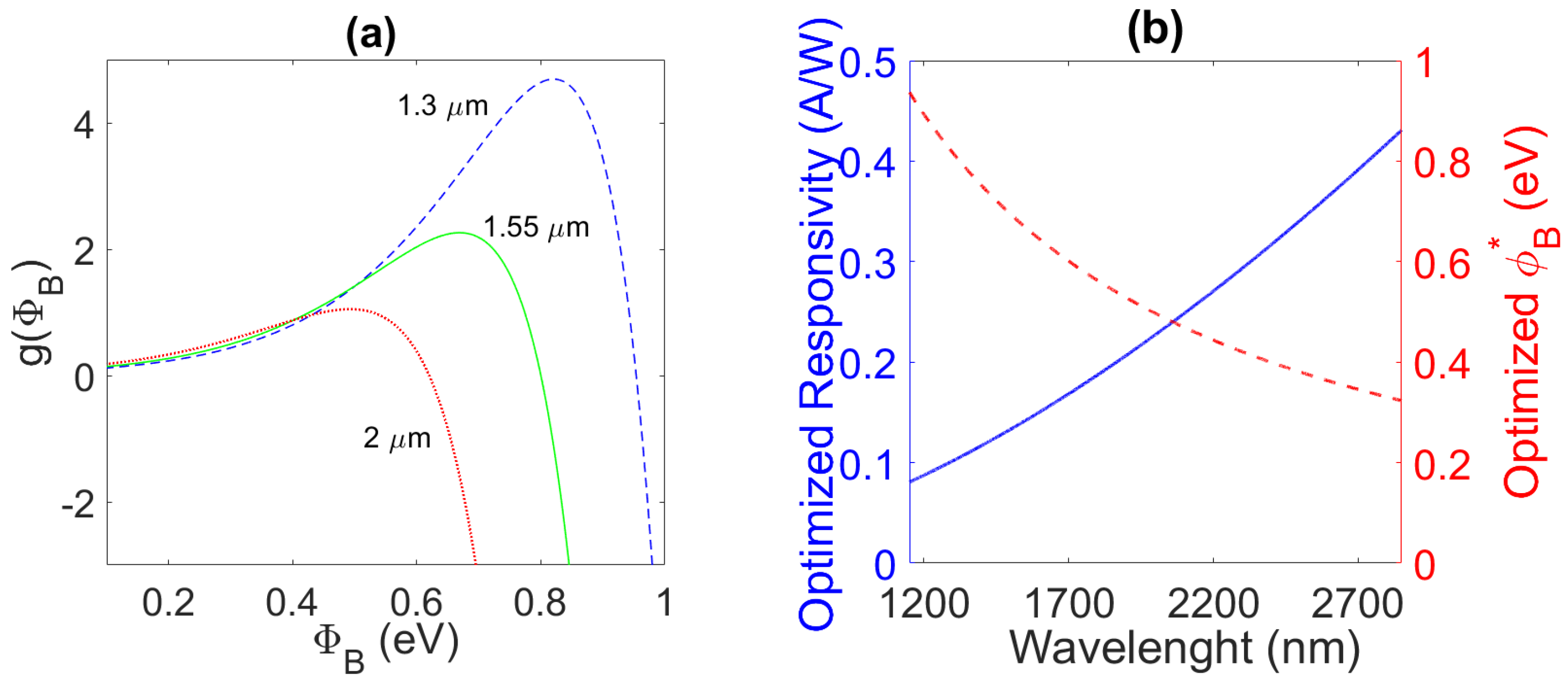
Figure 1a displays the behavior of
at 300 K for three different wavelengths, 1.3 μm, 1.55 μm, and 2 μm, showing the presence of a peak. By calculating the first and second derivatives of
we can find the value
of SBH corresponding to this peak:
We define
as the optimized SBH because it is the value at which the
R-to-
ratio is maximized. The dashed red line in
Figure 1b shows the optimized Schottky barrier
as a function of the wavelength. This behavior can be explained by considering that when the wavelength is reduced the photon energy
increases by diminishing the responsivity
R, as shown in Equation (
3), requiring a reduction of the
to maintain the maximized
ratio. In turn, the
reduction can be achieved by an increase of the optimized
, which decreases the amount of charge carriers able to overcome the Schottky barrier due to thermal effects. Even if the
increment also produces a decrease in responsivity, it is important to recall that while the
is characterized by an exponential decay as a function of
(
), the responsivity is characterized by a simple quadratic behaviour (
).
The substitution of Equation (
14) in Equation (
3) provides the responsivity when the ratio
is maximized (here we refer to it as the optimized responsivity), as shown by the blue solid line in
Figure 1b. Note that this optimized responsivity depends only on the SBH of the junction.
Figure 1b shows how the optimized responsivity is increased by increasing the wavelength owing to a drop in the optimized SBH
, providing values at room temperature of
A/W,
A/W, and
A/W at 1.3 μm, 1.55 μm, and 2 μm, respectively, as reported in
Table 1. If higher responsivities are required, they can be achieved by lowering the SBH but at the expense of the
.
3. Theoretical Results and Discussion
In this section we theoretically derive the SBH dependence on the bias applied to the junction in order to show how the graphene Schottky PDs based on different semiconductors could be optimized.
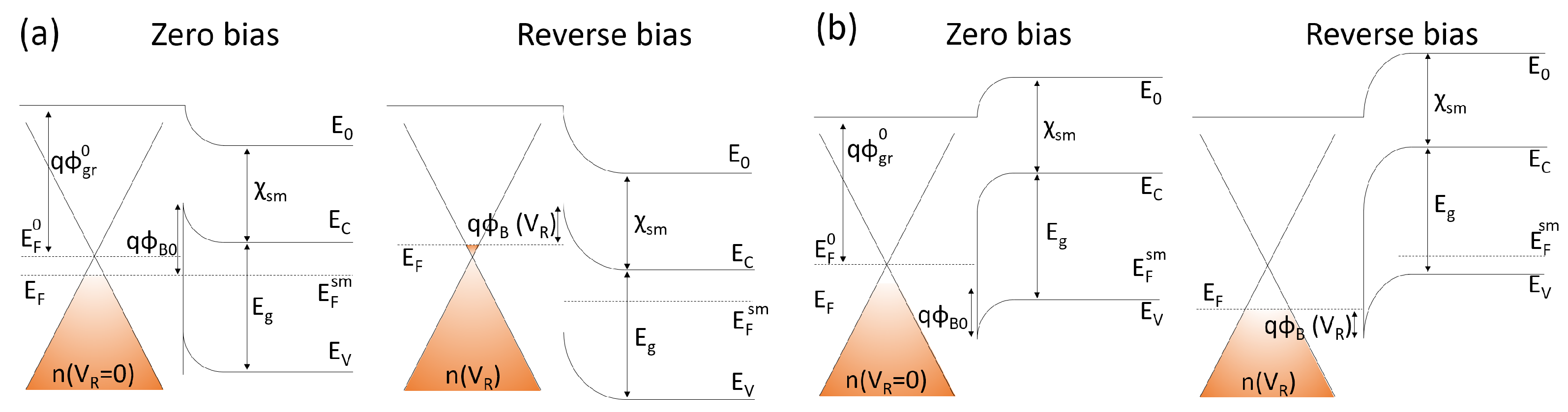
It is well-known that the SBH
of Schottky PDs can be determined by the two following equations (i.e., the Schottky–Mott relations) [
33]:
where
and
are, respectively, the electron affinity and the bandgap of the semiconductor and
is the difference between the vacuum level
and the Dirac point
, while the graphene Fermi level is
(
Figure 2). Therefore,
can be expressed as [
34]:
where
cm/s is the Fermi velocity,
ℏ is the reduced Planck constant, and
n is the carrier density in graphene. The carrier density
n not only depends on the graphene extrinsic doping
(defined positive and negative for p-type and n-type graphene doping, respectively) but also on the thermal contact with the semiconductor. Indeed, when a p-doped graphene (
) is transferred onto the semiconductor, the space charge
in the depletion region induces an opposite charge
in the graphene layer. This creates additional charge carriers, modifying the carrier density, which becomes
. The expression of the space charge
when the region is completely depleted is
, where
and
N are the dielectric permittivity and the doping density of the semiconductor, respectively, while
is the built-in potential. Moreover, by applying a reverse voltage, the charge per unit area in the graphene becomes
, providing a carrier density:
where the signs minus and plus are for n- and p-type semiconductors, respectively. Equation (
18) replaced into Equation (
17) and then in Equation (15) or (16) gives the desired dependence between the SBH and the reverse bias
.
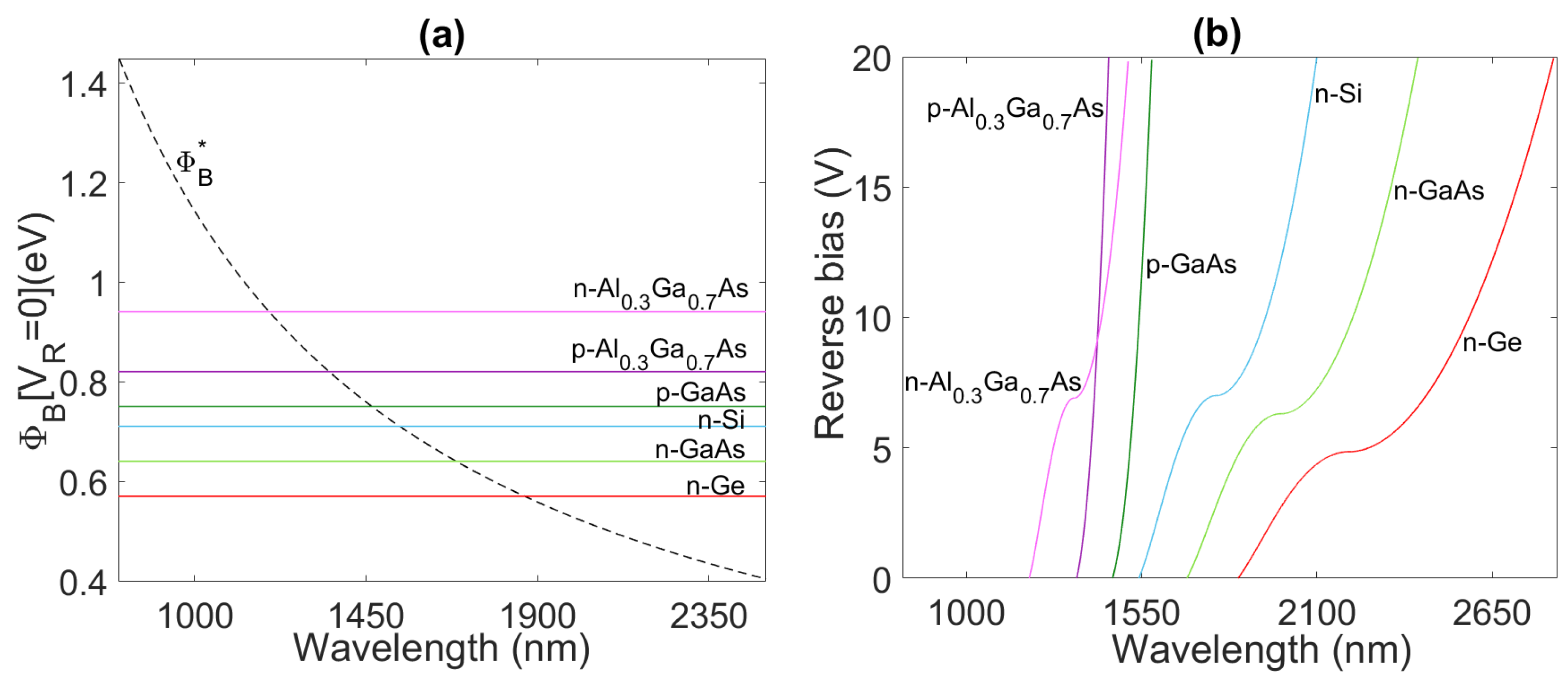
In
Table 2 we report the bandgap energy and the electron affinity for various semiconductors and the SBH at zero bias
, calculated through Equation (15) or (16) when
. The values of
were evaluated by considering a graphene work function
eV [
35,
36], a built-in potential
V, an initial SLG extrinsic p-doping
cm
, and a low doping of the semiconductors
cm
.
Figure 3a shows the intersections between these values of SBH
for different semiconductors and the curve of the optimized
at room temperature (given by Equation (
14)), suggesting the working wavelength to achieve the highest
ratio for each material. In the range of wavelengths where
>
, the SBH can be lowered down to its optimal value as in Equation (
14) by simply applying a specific reverse bias
to the junction.
By inverting Equation (
18) and using Equation (
17) and Equation (15) or (16) it is possible to calculate, for each wavelength and for each semiconductor, the values of the reverse voltage
such that
. We report this plot in
Figure 3b by considering a maximum reverse bias of 20 V. It is interesting to observe that within this limit, graphene Schottky PDs based on p-Al
0.3Ga
0.7As and p-GaAs can be optimized only in a narrow window of the NIR spectrum, whereas n-Si can be optimized in a broader range, including at 1.55 μm where only a small reverse voltage
V for maximizing the
ratio is required. Indeed, at a reverse voltage of
V the
eV of the graphene/n-Si junction can be reduced to its optimum value of
m) = 0.71 eV. In contrast, p-GaAs requires a higher reverse voltage of 12 V to maximize
. Finally, n-Ge stands out among the analyzed semiconductors in view of the possibility to be employed over a region of the NIR spectrum above 2 μm. The range of wavelengths where
can be optimized for various semiconductors, by applying a reverse bias up to 20 V, is summarized in
Table 3.
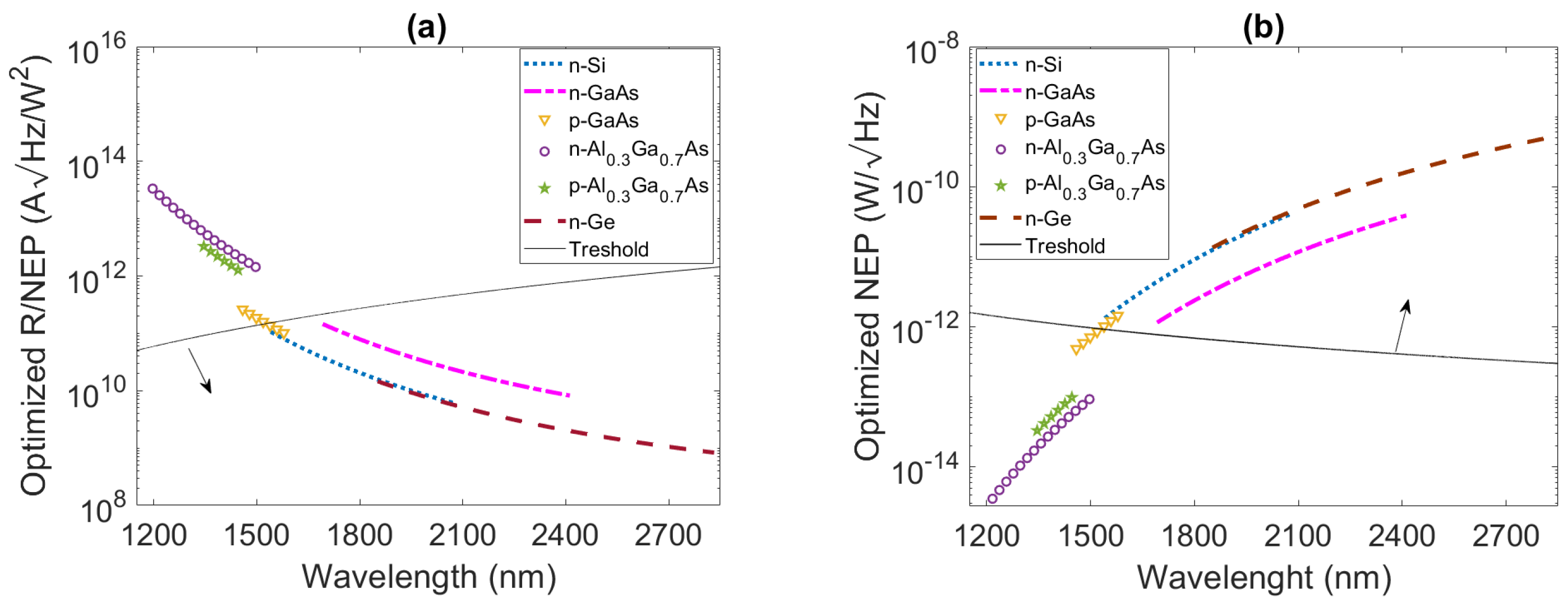
In
Figure 4a,b we report the values of the quantities of interest in this work—the
ratio and the optimized
—for all the examined semiconductors by considering a graphene circular area with radius of 500 μm and a PD closed on a load resistance of 10 M
. We compute these optimized quantities through Equation (
14) substituted into Equations (
3) and (
12). Recall that the results shown in
Figure 4 are valid when the condition in Equation (
8) is fulfilled. In order to verify it, we consider the dark current
one order of magnitude higher than
(
), and we calculate both optimized
and
by Equation (
12). The solid black lines drawn in
Figure 4a,b represent the validity thresholds of our discussion: graphene Schottky PDs can be optimized in terms of
ratio at a given wavelength by means the use of semiconductors placed below and above the solid black lines drawn in
Figure 4a,b, respectively. These thresholds depend on the load resistance
, the SBH
, and the graphene active area
, as is clearly shown by Equation (
8). We discover that in the case analyzed here, only graphene/n-Si, graphene/n-Ge, and graphene/n-GaAs Schottky PDs can be suitable for this optimization procedure. Although Si is typically used for visible detection, analysis shows that graphene/n-Si Schottky PDs with a maximized
ratio could be adopted for detecting sub-bandgap NIR wavelengths with responsivity and
of 133 mA/W and 500 fW/
at 1.55 μm, respectively. These devices provide low NEP, enabling their employment for power monitoring and lab-on-chip applications. Note that the predicted responsivity of graphene/n-Si PDs is higher than that reported for NIR Si PDs based on bulk-defect-mediated absorption. Indeed, taking advantage of mid-gap defects introduced into Si ring and disk resonators, Ackert et al. reported a responsivity of only 23 mA/W at
V [
37] and 45 mA/W at
V [
38] at 1560 nm, respectively. On the other hand, if the inter-band absorption of Ge is typically used for detecting the wavelength of 1.55 μm for telecommunications applications, graphene/n-Ge Schottky PDs could allow the detection of wavelengths longer than 1.55 μm, where the the Ge inter-band absorption suddenly decreases. Indeed, graphene/n-Ge Schottky PDs with optimized
ratio show a responsivity and
of 227 mA/W and 31 pW/
at 2 μm, respectively, enabling their employment in environment monitoring applications. The predicted responsivity of graphene/n-Ge PDs is higher than that reported for NIR Ge PDs based on the introduction of tin (Sn) atoms in the Ge lattice. Indeed, with a substitutional Sn concentration of
, Ge-based PDs are able to absorb optical radiation at 2 μm but provide a limited responsivity of only 20 mA/W [
39]. Note that NEP depends on many parameters, such as graphene’s optical absorbance, the graphene area in contact with the semiconductor, and the temperature. Among these, particular attention should be paid to the temperature, which appears in the exponential argument of the dark current (Equation (
4)), which in turn affects the NEP (Equation (
12)). As an example, in a graphene/n-Si Schottky PD we evaluated this by increasing the temperature of 1
C with respect to the room temperature, and an increase in optimized NEP below
could be achieved at any wavelength in the range of interest for this junction. As reported in
Figure 4a,b, semiconductors such as n-Si, n-Ge, and n-GaAs can be exploited at room temperature for the realization of optimized graphene-based Schottky PDs in the spectral range from 1955 to 2080 nm with a responsivity from 219 to 245 mA/W (
Figure 1b); however, while n-GaAs would be characterized by a lower NEP, n-Si and n-Ge would have the advantage of a better compatibility with CMOS technology.


