Article

Energy-Efficient Amplifiers Based on Quasi-Floating Gate Techniques

by
Antonio Lopez-Martin
1,*,
Maria Pilar Garde
1,
Jose M. Algueta-Miguel
1,
Javier Beloso-Legarra
1,
Ramon G. Carvajal
2 and
Jaime Ramirez-Angulo
3
1
Institute of Smart Cities, Universidad Pública de Navarra (UPNA), Campus Arrosadia, 31006 Pamplona, Spain
2
Department of Electronic Eng., School of Engineering, University of Seville, 410092 Sevilla, Spain
3
Klipsch School of Electrical Engineering, New Mexico State University, Las Cruces, NM 88003, USA
*
Author to whom correspondence should be addressed.
Appl. Sci. 2021, 11(7), 3271; https://doi.org/10.3390/app11073271
Submission received: 26 February 2021 / Revised: 30 March 2021 / Accepted: 31 March 2021 / Published: 6 April 2021

Abstract

:
Energy efficiency is a key requirement in the design of amplifiers for modern wireless applications. The use of quasi-floating gate (QFG) transistors is a very convenient approach to achieve such energy efficiency. We illustrate different QFG circuit design techniques aimed to implement low-voltage, energy-efficient class AB amplifiers. A new super class AB QFG amplifier is presented as a design example, including some of the techniques described. The amplifier has been fabricated in a 130 nm CMOS test chip prototype. Measurement results confirm that low-voltage, ultra-low-power amplifiers can be designed, preserving, at the same time, excellent small-signal and large-signal performance.

1. Introduction

Today, we are facing significant challenges in the design of electronic circuits. Many emerging wireless connectivity and Internet of Things edge computing applications require ultra-low-power wireless devices providing high performance in both indoor and outdoor environments. Energy efficiency is mandatory in such applications in order to increase battery lifetime. In fact, due to maintenance costs, battery replacement or manual recharge becomes impractical or even unfeasible in several scenarios with hard-to-reach wireless nodes (e.g., large civil infrastructures, vast natural ecosystems or implantable medical devices), requiring energy-autonomous wireless devices with batteries lasting several years. In some cases, the limited and often intermittent residual energy harvested from the environment (light, thermal gradients, vibrations, etc.) must be enough to operate the wireless device [1].
Aside from this, modern nanometer integrated circuit (IC) processes pose further challenges since device scaling directly impacts electronic design. Intrinsic gain reduction degrades DC gain. Supply voltage lower than 1 V becomes commonplace to reduce power consumption and to avoid gate oxide breakdown of nanometer devices. To complicate things, transistor threshold voltage cannot scale at the same rate as the supply voltage to keep subthreshold leakage currents low, so the available voltage swing reduces [2].
Preserving circuit performance in these demanding scenarios of energy scarcity and very low-voltage operation is a real challenge, and conventional circuit design techniques are often no longer valid in this framework. Innovative design techniques are required to meet these new demands. A critical block in modern mixed-signal ICs is the amplifier, which typically accounts for a significant percentage of the IC power budget [3]. Hence, designing high-gain wideband amplifiers operating with low supply voltage and low power requirements has become a major research topic. Conventional class A amplifiers are usually impractical under these constraints, since their maximum load current is limited by their bias current, so dynamic performance can only be improved at the expense of increased static power. These days, class AB amplifiers are preferred for low-voltage, low-power applications, since they allow maximum dynamic currents not bound by the quiescent currents [4]. However, providing class AB operation to the amplifier may degrade other characteristics, such as minimum supply voltage requirements, tolerance to process, supply voltage or temperature (PVT) variations, stability or noise performance. Likewise, to achieve energy efficiency, it is important that the large dynamic currents provided by the class AB circuits are generated in the output branch, without requiring internal copies of these large currents. Therefore, careful design of class AB amplifiers is mandatory.
This paper deals with the design of low-voltage class AB CMOS amplifiers able to maximize performance, preserving, at the same time, energy efficiency. It will be shown that quasi-floating gate (QFG) transistors [5] represent an excellent choice to achieve these goals. The QFG technique allows independent control of static and dynamic operation of the transistor by using separate input terminals for DC bias and AC signals. This allows overcoming the tradeoff between dynamic performance and quiescent power consumption of class A topologies. Very low and accurately controlled quiescent currents can be achieved by properly setting the DC input level. At the same time, large dynamic currents can be provided, since signals are capacitively coupled to the high impedance gate node. Due to these advantages, QFG transistors have found widespread use in the design of amplifiers [5,6,7,8,9,10,11,12,13,14,15,16,17,18,19,20,21,22,23,24,25,26,27,28,29,30] but also in high-performance current mirrors [31,32,33,34,35], mixers [36,37], linearization of active resistors [38,39], DC offset cancellation servo loop circuits [40], bootstrapped switches [5], current conveyors [30,41,42,43], Voltage Feedback Operational Amplifiers (VFOAs) [44], Current Feedback Operational Amplifiers (CFOAs) [45], buffers [46,47,48,49,50,51], rectifiers [35,52], capacitance multipliers [35], transconductors [30,53,54,55], digital-based analog circuits [56], DC–DC converters [57], continuous-time filters [58,59,60,61], track and hold circuits [5], data converters [5,62], capacitive sensing interfaces [63], particle detectors [23] and retinal prosthesis [64], to name some representative applications.
The paper is organized as follows: Section 2 provides an overview of QFG transistors and their application to the design of amplifiers. Section 3 reviews various reported amplifier topologies based on QFG techniques. A new energy-efficient class AB amplifier designed and fabricated in a 130 nm CMOS process is described in Section 4. A discussion on the results is provided in Section 5, and some conclusions are drawn in Section 6.

2. Quasi-Floating Gate Transistors

In this section, the fundamentals of QFG transistors are briefly presented, and their application to the design of low-voltage class AB amplifiers is discussed.

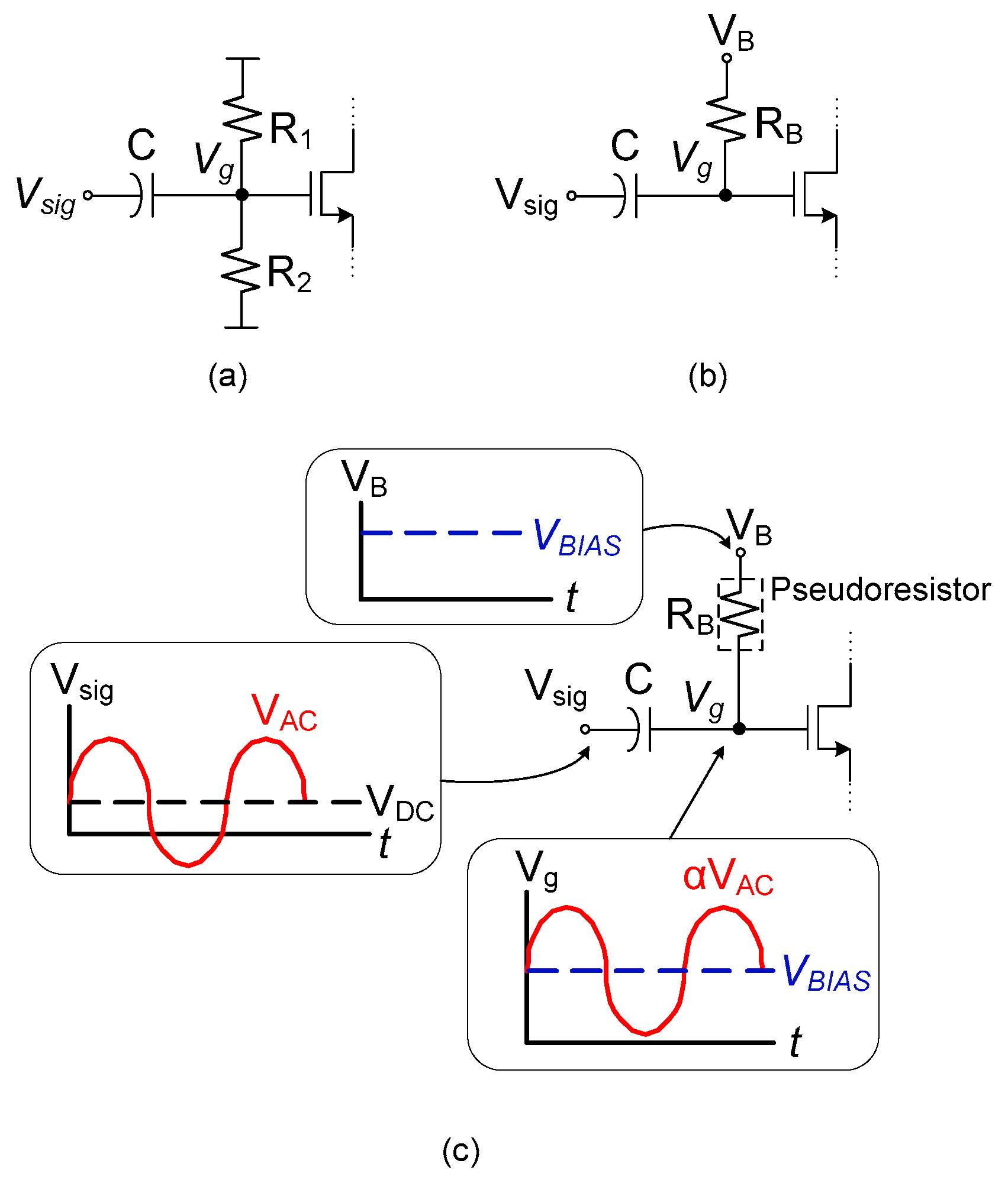
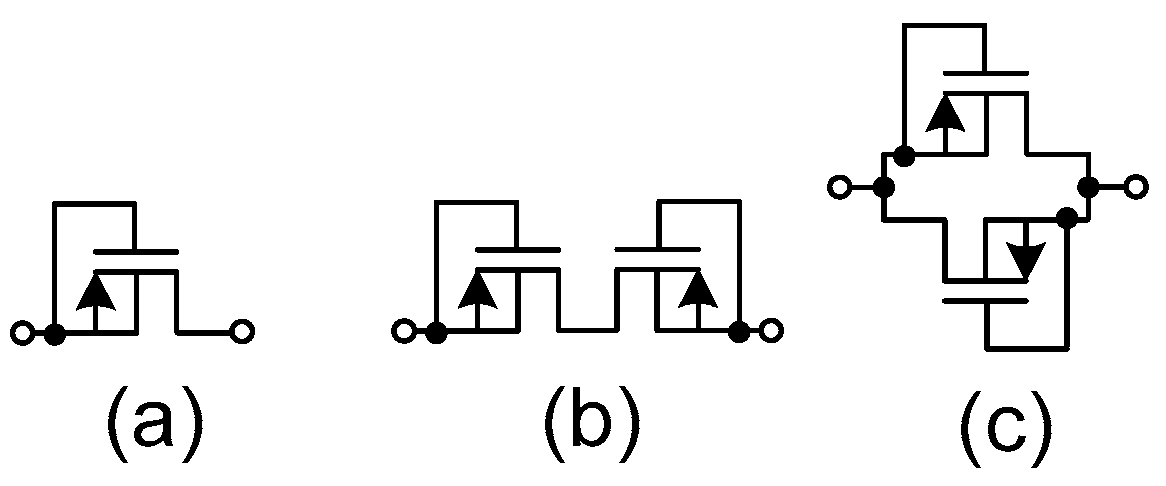
2.1. Wideband Capacitive Coupling Using Quasi-Floating Gate Transistors

Capacitive (or AC) coupling is widely used to isolate the DC bias setting circuit of active devices from the driving signal source. A typical example is shown in Figure 1a, where a resistive divider sets the quiescent gate voltage of the transistor. Coupling capacitor C blocks the input DC voltage and allows the input signal to pass through to the gate. A more general biasing scheme is shown in Figure 1b, where DC bias voltage VB is set using resistor RB. Note that the circuit of Figure 1a can be regarded as a particular case of Figure 1b, using the Thévenin’s theorem, where VB = (VDD − VSS)·R2/(R1 + R2) and RB = R1||R2.
The circuit of Figure 1b provides a first-order, low-pass filtering from input VB to the gate and a first-order, high-pass filtering from input Vsig to the gate, both with time constant RB·C. Due to the limited practical values of on-chip passive resistors and capacitors, this time constant cannot be too large. Hence, despite the name “AC coupling,” this technique is rather employed in ICs for RF narrowband signals with frequencies above the relatively large cutoff frequency of the high-pass input filter.
However, several relevant applications require processing of very low frequency signals (such as biomedical systems, structural health monitoring, geoenvironmental monitoring, etc.) or wideband signals with significant content at low frequencies (for instance, baseband processing circuits in a direct conversion receiver). In these cases, DC-blocking circuits able to allow near-DC frequency components pass through are required. An efficient approach to achieve the large time constant required is replacing resistor RB in Figure 1b by a pseudo-resistor (also known as quasi-infinite resistor, QIR) [6,7]. The resulting circuit is shown in Figure 1c, which is known as a QFG transistor [5]. Pseudo-resistors are small-area integrated devices that can provide extremely large incremental resistances (in the order of GΩ–TΩ) when they are properly biased. Therefore, very large RC time constants can be obtained using small capacitors that can be implemented on-chip.
From Figure 1c, the transfer functions from inputs VB and Vsig to Vg are:
V g ( s ) V B ( s ) = 1 1 + s τ
V g ( s ) V s i g ( s ) = α s τ 1 + s τ
with τ = RB·(C + Cg) as the time constant, Cg the parasitic capacitance at the gate terminal and α = C/(C + Cg). Note that input VB is low pass filtered with an extremely large time constant τ, so that the DC bias voltage VBIAS is set to the gate, and any AC noise or interference coming from this input is rejected. The signal at input Vsig is high pass filtered with the same time constant, so, in practice, only the DC level at this input is blocked. This input signal is also attenuated by a factor α, due to the nonzero parasitic gate capacitance Cg. The value of Cg sets the minimum required value for C to avoid excessive attenuation. Multiple-input QFG transistors can also be used [5], allowing weighted averaging of signals in a simple and compact way.
Note the different behavior of the circuit of Figure 1c for DC and AC small-signal and large-signal dynamic (or transient) operation. Capacitor C is an open circuit in DC, so the quiescent gate voltage is VgQ = VBIAS, since there is not current flowing through the pseudo-resistor. Hence, the bias point can be accurately set. For AC small-signal operation, the capacitor acts as a short circuit (more precisely, as an attenuator, due to the input capacitive divider), so that the AC gate voltage is vg = αvac, with vac the AC voltage at input Vsig. For transient operation with input frequencies larger than 1/τ (in practice from near DC), C acts as a floating battery with voltage VBIAS-VDC, with VDC the DC voltage at input Vsig. This is because C cannot be discharged rapidly through the pseudo-resistor. The signal is thus level-shifted by VBIAS-VDC and attenuated by factor α when it reaches the gate. In practice, nonlinearity of the pseudo-resistor may lead to nonlinear distortion and offset in the gate voltage. These issues are more relevant for large voltage swings at the pseudo-resistor terminals and depend on the implementation of the pseudo-resistors. Some of the most common fixed and tunable pseudo-resistors are shown in Figure 2 and Figure 3, respectively.
The simplest pseudo-resistor is a diode-connected PMOS transistor operating in deep subthreshold, as shown in Figure 2a [5,35,36]. It is very compact, but the resistance obtained cannot be modified once fabricated, and it is very sensitive to PVT variations. Moreover, the I–V characteristics are asymmetric, so it becomes nonlinear for large voltage swings. These drawbacks are usually of minor concern when the pseudo-resistor is used in high-gain amplifiers operating in negative feedback, as long as the resistance remains high enough for the QFG transistor to process the lowest frequency of the input signal Vsig in Figure 1c. When symmetric I–V characteristics are required, elementary devices can be mirrored either in series or in parallel, as shown in Figure 2b,c, respectively, for the case of two elements [8]. The series connection is useful when large resistance values for wide voltage ranges are needed.
Some applications require tunable pseudo-resistors, where tuning can be achieved using a DC voltage [8,12] or a DC current [13], as shown in Figure 3. Further details and examples of pseudo-resistors can be found in [8].

2.2. Application of QFG Transistors to Energy-Efficient Amplifier Design

Figure 4 illustrates various techniques based on QFG transistors that can be exploited to achieve low-voltage, energy-efficient amplifiers. They are described below.

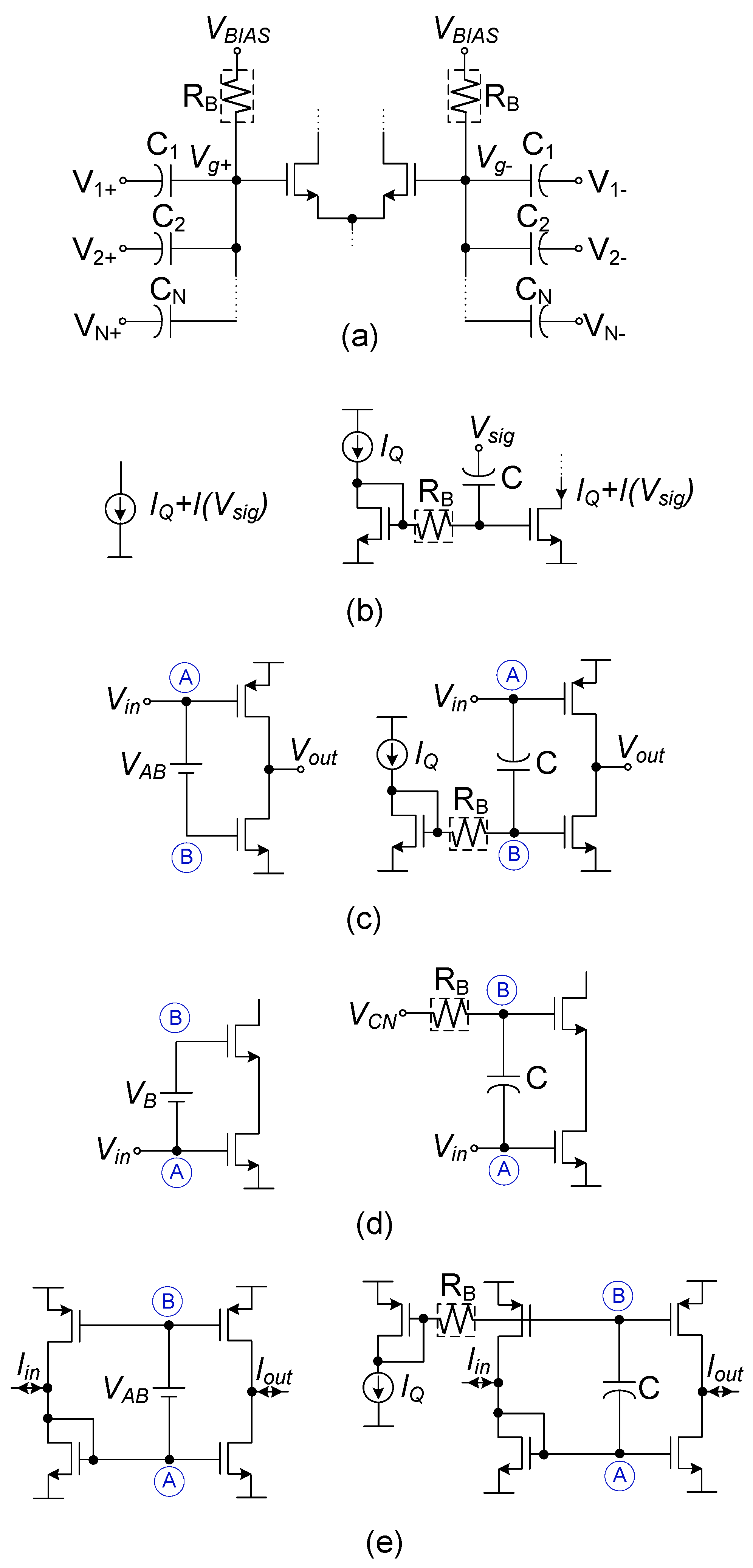
2.2.1. QFG Input Differential Pair

A QFG differential pair can be used at the input of the amplifier to get AC coupling, as shown in Figure 4a, where the general case of N inputs is depicted [5]. Assuming matched input capacitors Ck, the differential AC voltage at the gates vGd is a weighted averaging of the AC differential inputs vkd = vk+vk- set by Ck/CT capacitor ratios:
v G d = k = 1 N C k C T v k d
with Ck as the coupling capacitance of the k-th input and CT as the total capacitance at each gate node, which is approximately
C T k = 1 N C k + C G S + C G D + C G B + C P R
with CPR as the parasitic capacitance of the pseudo-resistor at the gate node. Usually, the first term in Equation (4) is dominant, so all the parasitic terms are negligible. Frequently, two-input QFG transistors are used to provide not only capacitive input coupling but also capacitive feedback. Various implementation examples are presented in Section 3.

2.2.2. Adaptive Bias Current Source

Figure 4b shows how a QFG transistor can be used to implement an adaptive bias current source. In quiescent operation (Vsig = 0), the circuit works as a current mirror and the quiescent output current is accurately set to IQ despite PVT variations. This current may be very low to save quiescent power. However, in dynamic operation (Vsig≠0), large output currents not limited by IQ can be generated, due to the AC coupling of Vsig.

2.2.3. Class AB Output Stage

A basic scheme of a class AB output stage is shown at the left side of Figure 4c. A floating battery VAB allows biasing the NMOS transistor and transfers input signal variations from node A to node B, providing output currents larger than the quiescent current. A QFG implementation is shown at the right side of Figure 4c, where the circuit of Figure 4b is used as active load of the input transistor, with Vsig = Vin. Note that the QFG technique allows an optimal implementation of the floating battery, since it does not influence the biasing of the NMOS transistor, which is set by a matched diode-connected transistor, as in a class A topology. The value of VAB can be either positive or negative; it is adapted to the supply voltage employed, preserving the quiescent gate voltages. This is not the case in conventional implementations of VAB using, e.g., diode-connected transistors or resistors biased by DC current sources [65]. Moreover, the QFG implementation of VAB does not require additional supply voltage or quiescent power and does not add extra nodes.

2.2.4. Dynamic Cascode Biasing

In class AB amplifiers, cascode transistors may restrict the VDS voltage of the transistors that generate the large dynamic currents, making these transistors enter ohmic region and limiting slew rate. To avoid this effect, dynamic biasing of the cascode transistors is required. It is typically done as shown on the left side of Figure 4d. A floating battery VB transfers a level-shifted version of the input signal in A to node B, so that the cascode gate voltage increases for large signals, increasing the VDS of the input transistor. Again, an efficient implementation of the floating battery can be made by using a QFG cascode transistor, as shown on the right side of Figure 4d. As before, the implemented value of VB is not fixed; it is the difference between the quiescent cascode bias voltage VCN and the quiescent input voltage, so it is insensitive to PVT variations. As before, no extra quiescent power or supply voltage requirements are needed.

2.2.5. Class AB Current Mirrors

Current mirrors are widely used in amplifier design as current followers, i.e., to convey currents from a low-impedance input node to a high-impedance output node. For instance, they are used in current mirror (symmetric) amplifiers to convey (and optionally scale) the differential pair current to the output node. When these current mirrors must process bidirectional signal currents, class AB operation is required to achieve a class AB amplifier [22]. A schematic diagram of a class AB current mirror is shown on the left side of Figure 4e. Again, a floating battery VAB translates signal variations from node A to B, allowing dynamic currents larger than the quiescent currents. A QFG implementation is shown in Figure 4e [31], which consists, basically, on the replacement of the PMOS current sources on the left side by a two-output adaptive current source, like in Figure 4b. As before, this implementation features accurate quiescent currents not dependent on PVT variations. VAB is set by the difference between quiescent voltages at nodes A and B and can be either positive or negative. No extra supply voltage or quiescent power is required.

3. Energy-Efficient Amplifiers Based on QFG Techniques

In this section, the application of the QFG techniques and circuits to low-voltage power-efficient amplifiers is illustrated.

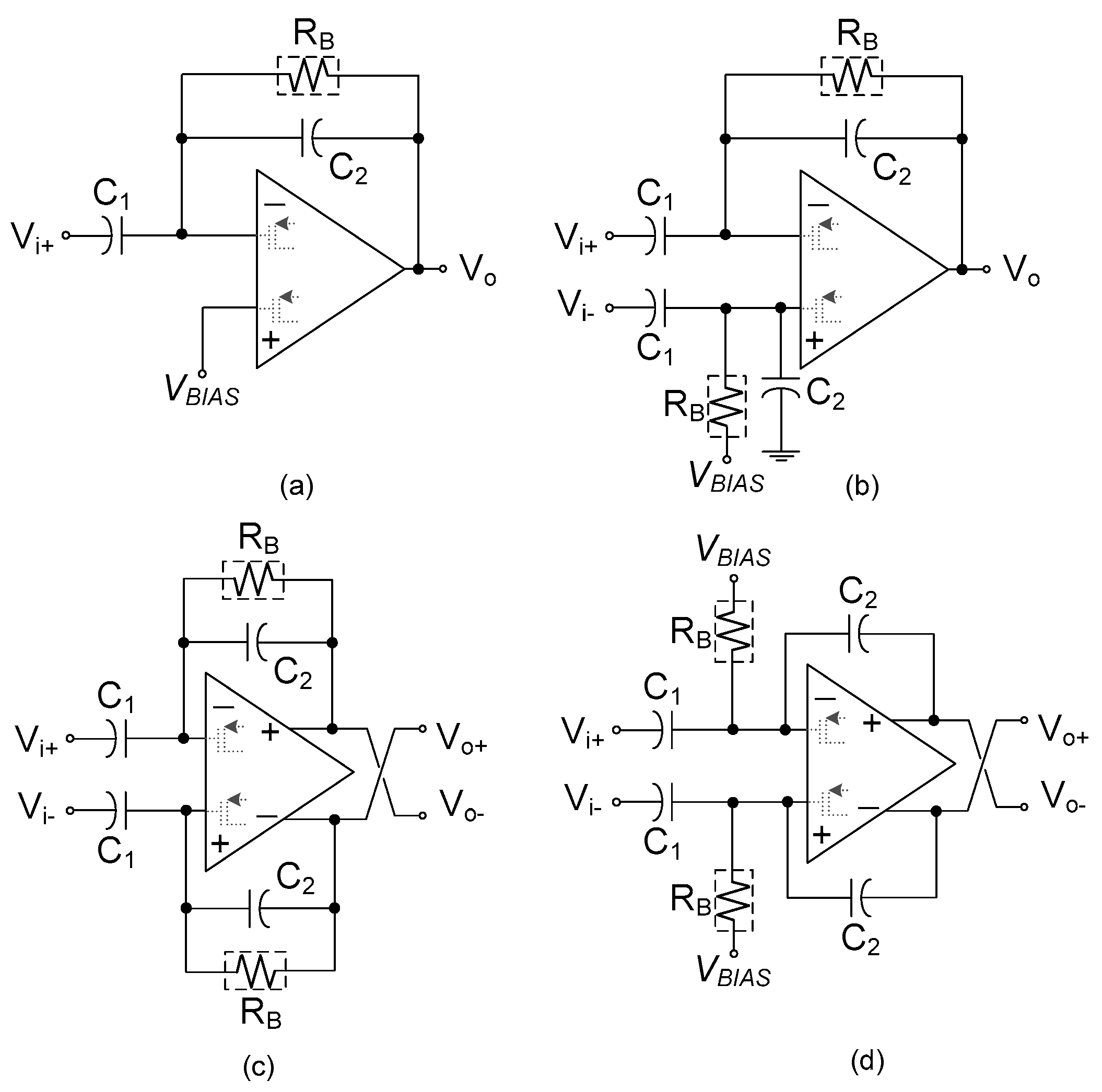
3.1. AC-Coupled Amplifiers

AC-coupled amplifiers allow accurate amplification (set by capacitance ratios), providing, at the same time, blocking of near-DC inputs. They are widely used to remove electrode offsets in physiological signals and also in interface circuits for monitoring of seismic activity or mechanical vibrations. For instance, electrode–skin interfaces may lead to offsets larger than 1 V [6], which can limit dynamic range and even saturate the amplifier if they are not removed.
Efficient AC-coupled amplifier implementations can be made using QFG input transistors, as shown in Figure 5 [5,6]. The circuit of Figure 5a can be used for singled-ended input and output, while Figure 5b provides single-ended output for differential inputs. The circuits of Figure 5c,d are fully differential topologies. Note that one (Figure 5a) or two (the other topologies) two-input QFG transistors are employed at the amplifier input. The QFG input capacitor C1 goes to the input terminal, and the other QFG input capacitor C2 is connected to the output. The midband gain is, in all cases, C2/C1. Note that the QFG pseudo-resistor is connected to the output in Figure 5a–c to provide DC-negative feedback. This is not the case in Figure 5d, where the amplifier is in open loop in DC. Hence, adequate design is required, in this case, to avoid saturation of the output [5]. An advantage of Figure 5d is that the amplifier DC input VBIAS can be set to a supply rail, so the circuit can work with ultra-low-supply voltages. Another advantage is that the pseudo-resistor experiences little voltage swings, so a simple pseudo-resistor implementation can be used [5].

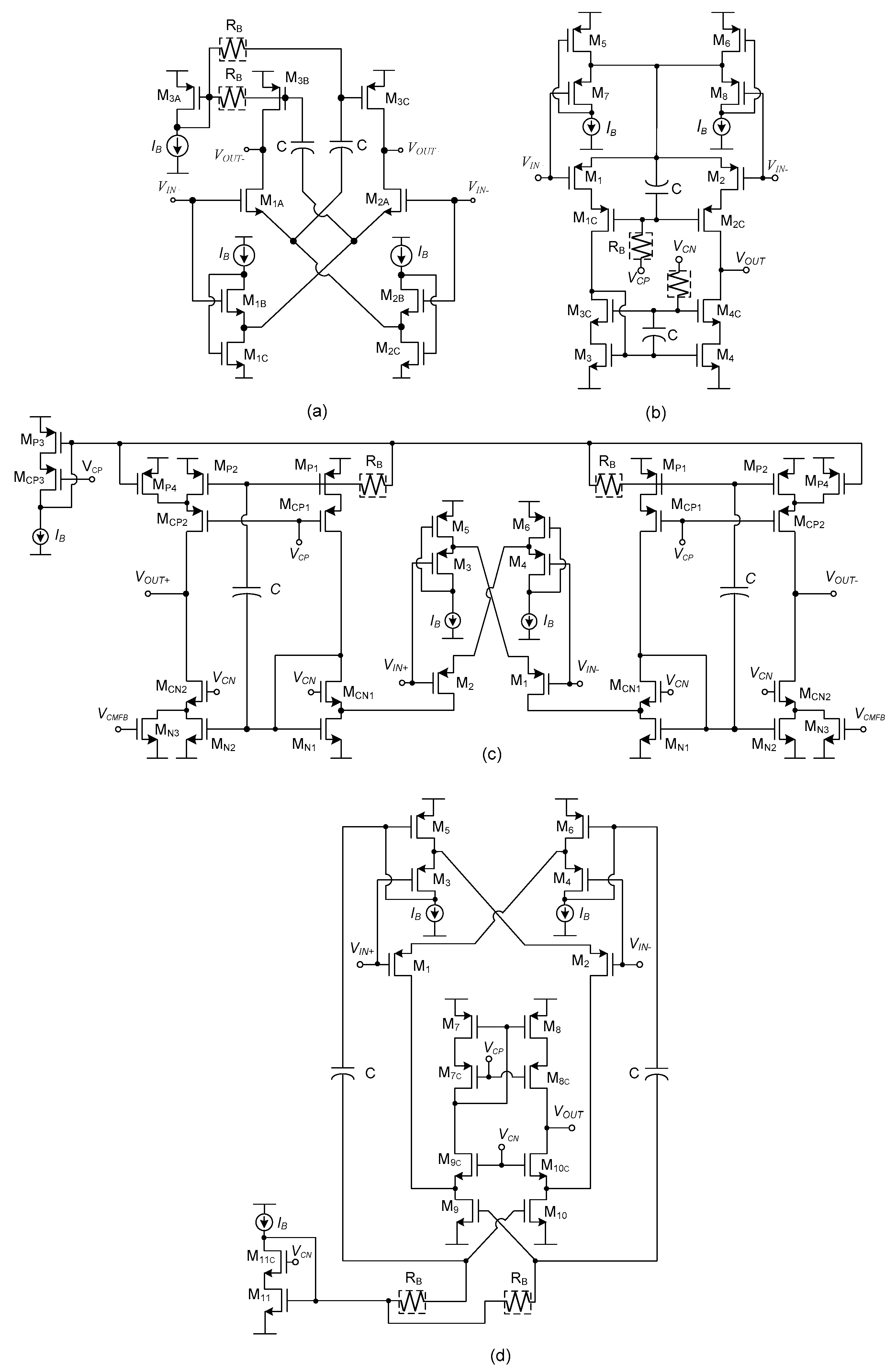
3.2. Single-Stage Class AB Amplifiers

In terms of energy efficiency and silicon area, single-stage amplifiers are the best option, since they are load-compensated [65] and can feature near-optimal current efficiency if properly designed [5]. The single-stage differential pair amplifier provides simplicity and high current efficiency. A class AB QFG fully differential implementation can be achieved, as shown in Figure 6a [17], where the common-mode feedback (CMFB) circuit is not shown. Transistors M1A–M2A are adaptively biased using two cross-coupled DC level shifters implemented by flipped voltage followers (FVF) [66] M1B–M1C and M2B–M2C. This adaptive biasing doubles the gain-bandwidth product (GBW) and allows dynamic currents in M1A and M2A larger than IB. The active load is implemented by adaptive QFG current sources M3B and M3C, like in Figure 4b.
To provide more DC gain, preserving current efficiency, a class AB telescopic cascode implementation can be used, as shown in Figure 6b [20]. In this case, adaptive biasing of the differential pair is also implemented by two FVFs, but in this case, the FVF outputs are connected. Hence, both FVFs act as a winner-take-all (WTA) circuit [67], setting the maximum of the input voltages level shifted by a DC voltage VB = VSG7,8Q to the common source of M1–M2. This, again, allows differential pair currents much larger than the quiescent current IB. Dynamic QFG cascode biasing, as in Figure 4d, is used to avoid that transistors M1–M2 and M3–M4 enter triode region when such large dynamic currents are generated.
Despite the high power efficiency of the amplifiers of Figure 6a,b, output swing is limited, since the input transistors are at the output branch. Alternative single-stage configurations with increased output swing can be obtained by including a current follower or a current amplifier to convey (and eventually scale) the differential pair current to the output terminal. This current follower/amplifier can be implemented by either a current mirror or a common-gate configuration, leading to the current-mirror (symmetric) and folded cascode amplifiers, respectively [22]. An example of class AB current mirror amplifier is presented in [23]. If high gain is required, a cascode current mirror implementation can be used, as shown in Figure 6c, in fully differential version (CMFB circuit not shown) [22]. The same adaptive biasing of Figure 6a is used, and two class AB cascode current mirrors, following the idea of Figure 4e, convey the current of the input transistors to the output terminals. A class AB folded cascode topology is shown in Figure 6d [19]. The same adaptive bias circuit is used for the input pair, and the NMOS current sources at the folding nodes are replaced by adaptively bias current sources following the scheme in Figure 4b. Dynamic biasing of cascode transistors can be used in Figure 6c,d to prevent slew rate (SR) degradation, as done in Figure 6b.

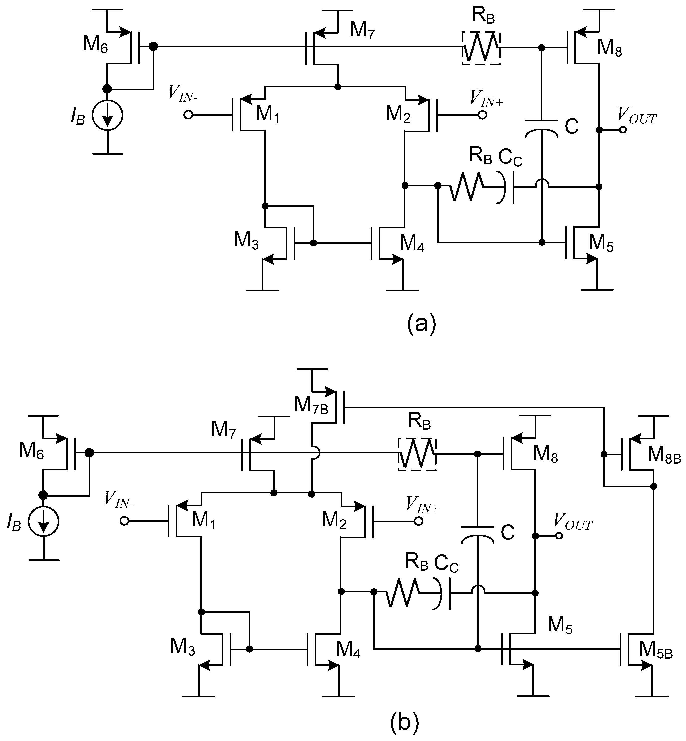
3.3. Multistage Class A/AB Amplifiers

When both high gain and high output swing are required, usually multistage amplifier topologies are employed. For instance, the conventional Miller amplifier can provide class AB output by employing the circuit of Figure 4c at the output stage [25]. The resulting circuit is shown in Figure 7a, yielding output currents much larger than the bias current IB and increasing GBW, due to the extra transconductance provided by M8. It is denoted as a class A/AB amplifier, since the input stage operates in class A and the output stage in class AB. Other examples of class A/AB amplifiers can be found in [26,27].

3.4. Multistage Class AB/AB Amplifiers

A drawback of class A/AB amplifiers is that the input stage can limit slew rate if it is not able to drive the compensation capacitor fast enough. To solve this drawback, class AB operation can also be included at the input stage, leading to class AB/AB topologies. Any of the class AB circuits of Figure 6 can be used at the first stage to this aim. A slightly different approach is shown in Figure 7b [28], where a scaled replica of the current in the output transistor M5 is fed back to the differential pair. Another example of class AB/AB QFG implementation can be found in [29].

4. Design Example: Super Class AB QFG Amplifier in a 130 nm CMOS Process

To illustrate the different approaches that can be employed to design energy-efficient amplifiers, a novel topology is presented in this section. It combines various techniques to achieve high performance and very low power consumption. Some of these techniques have been described above and some others are introduced here.

4.1. Requirements and Figures of Merit for Energy Efficiency

An ideal amplifier, in terms of energy efficiency, should achieve the highest small-signal and large-signal performance for a given (and small) quiescent current. A usual way to quantify these requirements is using two conventional figures of merit [68]. The first one is FoML = SR·CL/Isupply = ImaxL/Isupply, with SR as the Slew Rate, CL the load capacitance, ImaxL = SR·CL as the maximum load current and Isupply as the total quiescent current consumption. FoML quantifies the large-signal performance for a given Isupply. The second one is FoMS = GBW·CL/Isupply, which quantifies the small-signal performance for a given Isupply. A power-efficient amplifier should also maximize current utilization [69], defined as the portion of supply current delivered to the load, which is optimal when the large dynamic currents are generated directly at the output branch without internal replication of them.
An optimal choice in terms of energy efficiency is the so-named super class AB amplifiers [69]. They are single-stage topologies combining adaptive biasing at the input differential pair and nonlinear current amplifiers to convey and additionally boost the differential pair current to the output. Super class AB amplifiers can potentially achieve very large FoML, due to this double current boosting process, and can also achieve very large FoMS if the adaptive biasing and nonlinear current amplifiers employed provide enhanced transconductance. Moreover, current utilization is very high, as the large dynamic currents achieved are generated directly at the output transistors of the nonlinear current amplifier, right at the output branch.

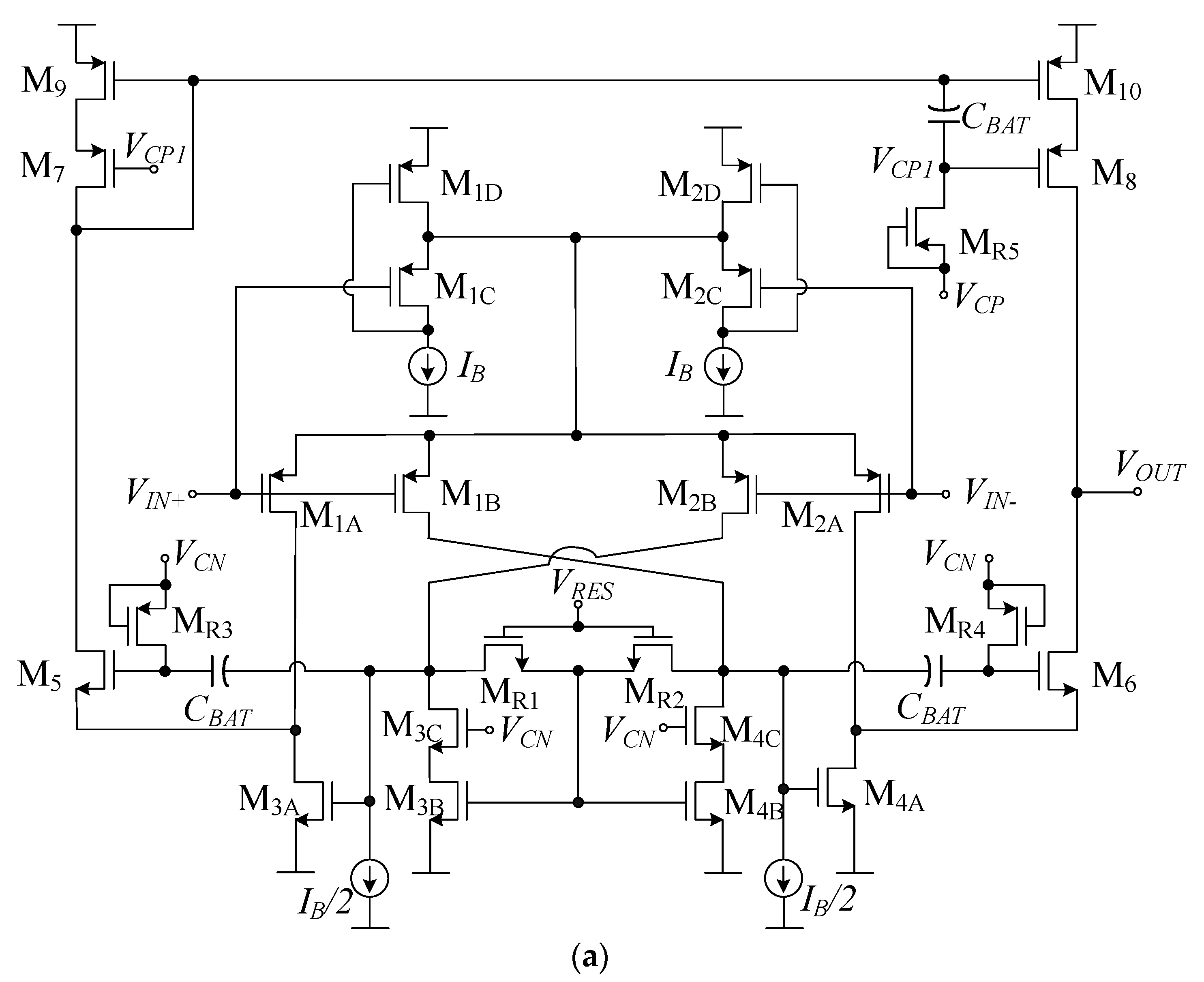
4.2. Proposed Super Class AB Amplifier

Figure 8a shows the proposed circuit, which is based on a recycling folded cascode topology [70]. The same adaptive bias circuit used in Figure 6b, formed by the FVFs M1C–M1D and M2C–M2D, is employed. In quiescent conditions, M1C–M2C have the same VGSQ as M1A, M1B, M2A and M2B, and, since they have also the same size, neglecting mismatch and channel length modulation, they set a quiescent current IB in M1A, M1B, M2A, and M2B. When a differential signal is applied, the largest (winning) input voltage level shifted by the VSGQ of M1C–M2C appears at the common source of M1A, M1B, M2A and M2B. Hence, currents in these transistors are not limited by IB, due to the large currents that can be provided by the FVFs.
The differential current amplifier employed to transfer and scale the currents in M1B and M2B to the output is a nonlinear cascode current mirror formed by M3A, M3B, M4A, M4B, M3C, M4C, M5 and M6. It employs local common-mode feedback [69] by transistors MR1–MR2 acting as tunable active resistors. When a large differential current appears in M1B–M2B, a large voltage drop appears in MR1–MR2, which creates a large current in either M3A or M4A, which reaches the output. Hence, this nonlinear current mirror provides an additional dynamic current boosting.
Current starving is implemented in Figure 8a by two DC current sources that subtract part of the DC input current to the NMOS current mirrors. For a fixed current mirror gain K, current starving allows for decreasing the quiescent current of the current mirror output, thus increasing the amplifier output resistance and DC gain [71]. However, here, current starving is used to increase K without increasing static power. The starving factor used is 0.5, so half of the bias current (IB/2) is subtracted. As a result, K can be doubled in Figure 8a for the same quiescent current consumption.
Adaptive biasing of cascode transistors M5, M6, M7 and M8 is provided using the QFG technique of Figure 4d to avoid M3A, M4A, M9 and M10 entering triode region for large dynamic currents (which would strongly degrade SR). The simple pseudo-resistor of Figure 2a is enough, in this case.

4.3. Circuit Analysis

Routine small-signal analysis of the circuit of Figure 8a leads to a transconductance
G m g m 1 A [ 1 + g m 3 A ( R D S | | r o 2 B ) ]
with gmi and roi as the small-signal transconductance and output resistance of transistor Mi, respectively, and RDS as the resistance of triode transistors MR1 and MR2, which is
R D S 1 β R 1 , 2 ( V R E S I B β 3 B V S S 2 V T H )
where βi = µCox(W/L)i is the transconductance factor of transistor Mi. The GBW is GBW = Gm/(2πCL), with Gm defined in Equation (5) and CL as the load capacitor. The small-signal gain is Gm·Rout, with Rout = gm8ro8ro10||[gm6ro6(ro4A||ro2A)] as the output resistance of the amplifier. Using the simple MOS square law, an approximate expression can be found for the SR:
S R β 3 A , 4 A 2 C L ( β 1 B , 2 B 2 β 3 B , 4 B A + R D S β 1 B , 2 B 4 A 2 ) 2
with A as the differential input signal amplitude. Note that SR is not limited by the bias current, as expected from a class AB amplifier. Practical values of SR are, however, lower, due to nonideal effects not considered in Equation (7).
Regarding thermal noise and noting that gm1A = gm1B = gm1C = gm2A = gm2B = gm2C, gm3A = gm4A, gm3B = gm4B and gm9 = gm10, the input-referred noise density is
V n , i n 2 ¯ = 2 δ k B T g m 1 A ( 2 + g m 3 B g m 1 A + g m I g m 1 A + 1 δ g m 1 A R D S + 1 g m 1 A g m 3 A R D S 2 + g m 9 g m 1 A g m 3 A 2 R D S 2 + 1 g m 3 A 2 R D S 2 )
with kB as the Boltzmann’s constant, T as the absolute temperature, gmI as the transconductance of the transistors implementing the IB/2 current sources and δ as a parameter that varies from 1/2 to 2/3 from weak inversion to strong inversion. Note that transistors in the output branch have little influence on the input-referred noise, due to the large gain, according to theoretical expectations.
Note, also, that decreasing bias voltage VRES increases RDS and, hence, increases gain, GBW and SR and reduces input-referred noise. Unfortunately, it also reduces phase margin, which can be approximated by
P M 90 ° tan 1 ( G B W f p N D ) 90 ° tan 1 [ g m 1 A g m 3 A ( R D S | | r o 2 B ) 2 C X C L ]
where fpND≈ −1/[2π(RDS||ro2B)CX] is the frequency of the lowest nondominant pole, and CX is the parasitic capacitance at the nodes where the gates of M3A and M4A are connected. Hence, a tradeoff between gain, GBW, SR, input-referred noise and stability exists for a given CL. Tuning VRES allows for optimally balancing these parameters and compensating for PVT variations.

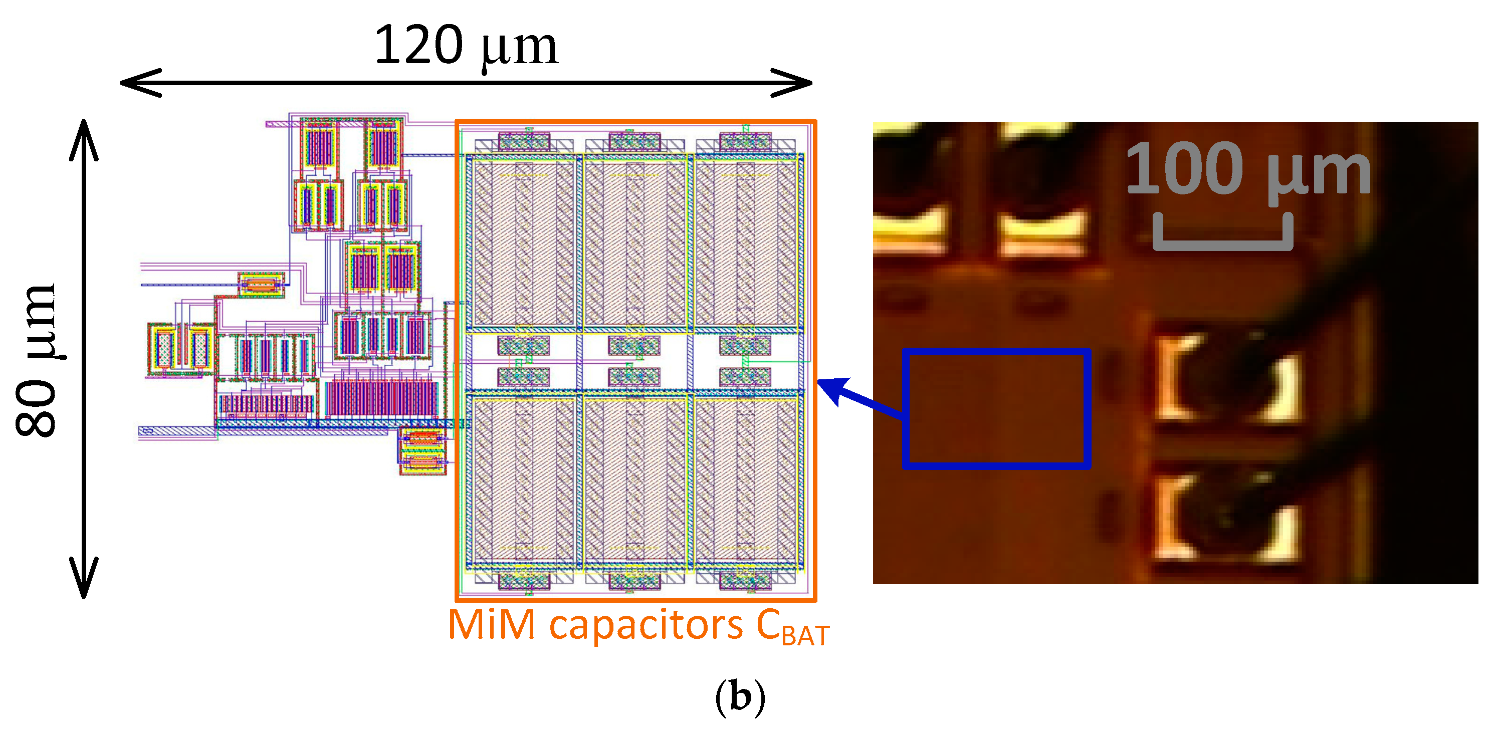
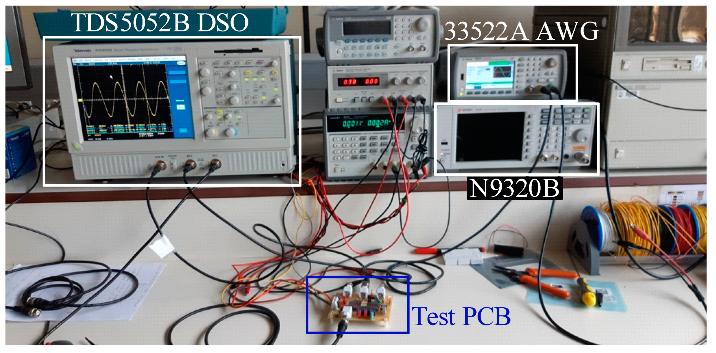
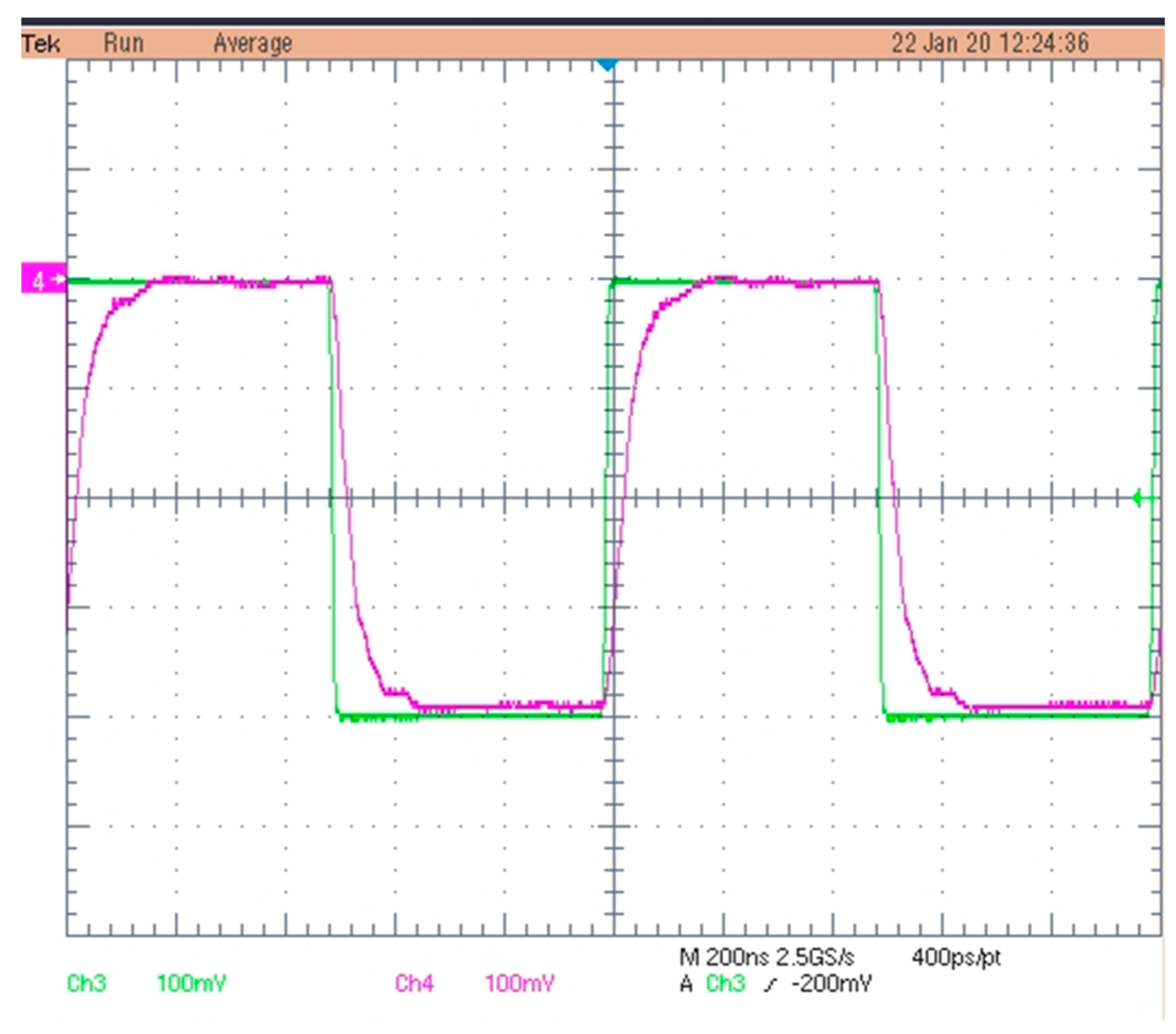
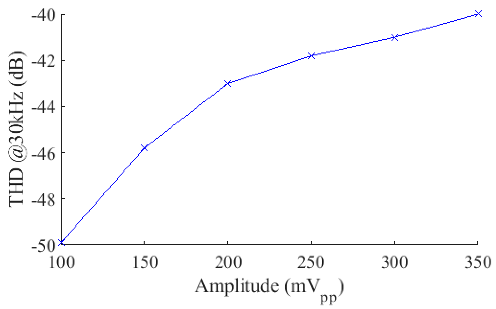
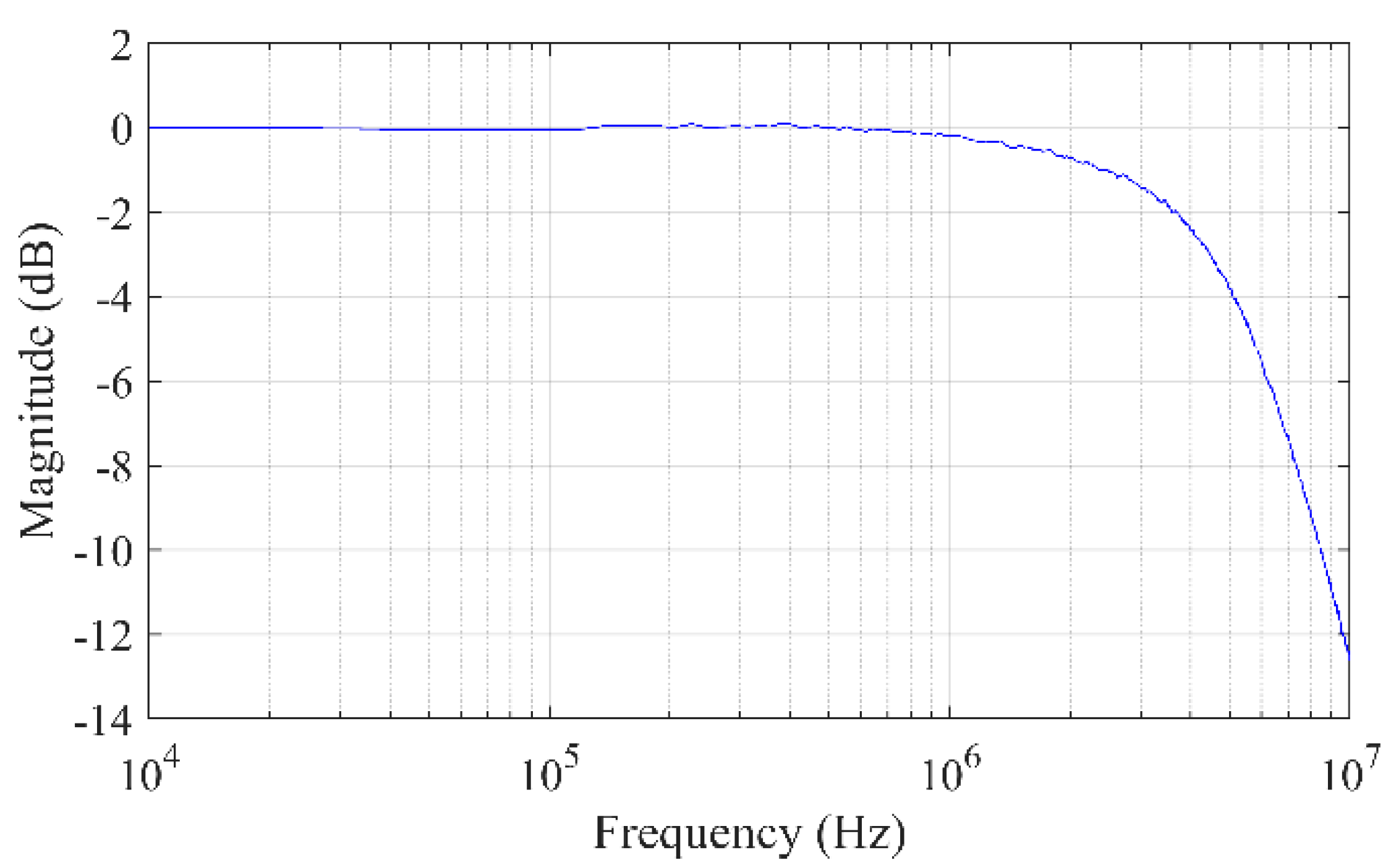
4.4. Measurement Results

A 130 nm CMOS technology was employed to fabricate a unity-gain, closed-loop version of the proposed super class AB amplifier of Figure 8a. Transistor aspect ratios W/L (in µm/µm) were 72/0.24 (M3A, M4A), 24/0.24 (M5, M6), 12/0.12 (M7, M8), 6/2 (MR1, MR2), 0.5/5 (MR3, MR4, MR5) and 12/0.24 for the rest. Three metal–insulator–metal (MiM) capacitors CBAT of 1 pF were employed. A microphotograph of the circuit is shown in Figure 8b, where the layout plot is also shown, since the surface of the die is opaque.
Supply voltages were ±0.5 V and IB = 3 µA. Cascode bias voltages VCP and VCN were −0.34 V and 0.3 V, respectively, and VRES was set to 480 mV. The measurement setup used is shown in Figure 9.
For transient response, the input signal was a 1 MHz 0.4 Vpp square wave, with a −0.2 V DC level generated by an Agilent 33522A arbitrary waveform generator, and the output was displayed in a Tektronix TDS5052B oscilloscope. Total load capacitance was 140 pF. Both the input and transient response are plotted in Figure 10. The measured SR values for the rising and falling edge were 5.7 V/µs and −7.1 V/µs, respectively. Figure 11 shows the measured total harmonic distortion (THD) using a 30 kHz input tone, whose amplitude varies from 100 mVpp to 350 mVpp. Note that THD is below 1% in all this range.
The frequency response was also measured (Figure 12) using a Keysight N9320B spectrum analyzer. Since an off-chip buffer was employed to avoid loading the analyzer, total load capacitance was CL = 120 pF. The cutoff frequency of the proposed OTA was 4.48 MHz, which corresponds approximately to the GBW, because of the dominant pole design.

5. Discussion

A summary of the main performance parameters of the amplifier is shown in Table 1, including parameters from other reported amplifiers for comparison. Since the fabricated amplifier is in unity-gain closed loop, open-loop performance parameters (DC gain, Phase Margin PM, Common-Mode Rejection Ratio CMRR and Power Supply Rejection Ratio PSRR) were obtained from post-layout simulations using BSIM4 MOSFET models and the Spectre simulator available in Cadence IC6.1.
Note that the proposed amplifier showed improved small-signal and large-signal performance just drawing 30 μA from the ±0.5 V power supply. A graphical comparison of FoML and FoMS with different reported amplifiers is shown in Figure 13, where the advantages of the proposed approach are evidenced. Note the good balance between both figures of merit, as deduced from their average value (FoMAVG) in Table 1. The main drawback of the proposed amplifier is the extra silicon area required for the capacitors CBAT, employed for dynamic cascode biasing, as can be seen in Figure 8b.

6. Conclusions

A comprehensive description of different circuit techniques based on QFG transistors and their application to energy-efficient amplifiers has been presented. Moreover, a new, low-power CMOS amplifier, using adaptive local common-mode feedback with current starving, WTA tail current biasing and QFG transistors for adaptive cascode biasing, has been proposed. Measurement results of the amplifier fabricated in a 130 nm process show very large SR and GBW, maintaining very low static power consumption. The amplifier can be applied in ultra-low-power switched capacitor systems and in general, when both large capacitive loads and low quiescent power are required.

Author Contributions

Conceptualization, A.L.-M. and J.R.-A.; methodology, A.L.-M.; software, M.P.G.; validation, M.P.G.; formal analysis, A.L.-M.; investigation, A.L.-M., J.M.A.-M. and J.R.-A.; resources, A.L.-M.; data curation, M.P.G. and J.B.-L.; writing—original draft preparation, A.L.-M. and M.P.G.; writing—review and editing, J.M.A.-M., J.B.-L., R.G.C. and J.R.-A.; visualization, M.P.G. and J.B.-L.; supervision, A.L.-M.; project administration, A.L.-M.; funding acquisition, A.L.-M. All authors have read and agreed to the published version of the manuscript.

Funding

This research was funded by AEI/FEDER, grant number PID2019-107258RB-C32.

Data Availability Statement

The data presented in this study are available on request from the corresponding author.

Conflicts of Interest

The authors declare no conflict of interest.

References

  1. Li, P.; Long, Z.; Yang, Z. RF Energy Harvesting for Battery-Less and Maintenance-Free Condition Monitoring of Railway Tracks. IEEE Internet Things J. 2020, 8, 3512–3523. [Google Scholar] [CrossRef]
  2. Bohr, M.T.; Young, I.A. CMOS Scaling Trends and Beyond. IEEE Micro 2017, 37, 20–29. [Google Scholar] [CrossRef]
  3. Svensson, C.; Wikner, J.J. Power consumption of analog circuits: A tutorial. Analog Integr. Circuits Signal Process. 2010, 65, 171–184. [Google Scholar] [CrossRef] [Green Version]
  4. Kim, J.; Song, S.; Roh, J. A High Slew-Rate Enhancement Class-AB Operational Transconductance Amplifier (OTA) for Switched-Capacitor (SC) Applications. IEEE Access 2020, 8, 226167–226175. [Google Scholar] [CrossRef]
  5. Ramirez-Angulo, J.; Lopez-Martin, A.J.; Carvajal, R.G.; Chavero, F.M. Very low-voltage analog signal processing based on quasi-floating gate transistors. IEEE J. Solid State Circuits 2004, 39, 434–442. [Google Scholar] [CrossRef]
  6. Harrison, R.R.; Charles, C. A low-power low-noise CMOS amplifier for neural recording applications. IEEE J. Solid State Circuits 2003, 38, 958–965. [Google Scholar] [CrossRef]
  7. Zou, X.; Xu, X.; Yao, L.; Lian, Y. A 1-V 450-nW Fully Integrated Programmable Biomedical Sensor Interface Chip. IEEE J. Solid-State Circuits 2009, 44, 1067–1077. [Google Scholar] [CrossRef]
  8. Guglielmi, E.; Toso, F.; Zanetto, F.; Sciortino, G.; Mesri, A.; Sampietro, M.; Ferrari, G. High-Value Tunable Pseudo-Resistors Design. IEEE J. Solid State Circuits 2020, 55, 2094–2105. [Google Scholar] [CrossRef]
  9. Pourashraf, S.; Ramirez-Angulo, J.; Lopez-Martin, A.J.; Carvajal, R.G.; Diaz-Sanchez, A. ±0.18-V supply voltage gate-driven PGA with 0.7-Hz to 2-kHz constant bandwidth and 0.15-μW power dissipation. Int. J. Circuit Theory Appl. 2018, 46, 272–279. [Google Scholar] [CrossRef]
  10. Wang, T.; Liu, L.; Peng, S. A Power-Efficient Highly Linear Reconfigurable Biopotential Sensing Amplifier Using Gate-Balanced Pseudoresistors. IEEE Trans. Circuits Syst. II Express Briefs 2015, 62, 199–203. [Google Scholar] [CrossRef]
  11. Deepu, C.J.; Zhang, X.; Liew, W.; Wong, D.L.T.; Lian, Y. An ECG-on-Chip with 535 nW/Channel Integrated Lossless Data Compressor for Wireless Sensors. IEEE J. Solid State Circuits 2014, 49, 2435–2448. [Google Scholar] [CrossRef] [Green Version]
  12. Rezaee-Dehsorkh, H.; Ravanshad, N.; Lotfi, R.; Mafinezhad, K.; Sodagar, A.M. Analysis and Design of Tunable Amplifiers for Implantable Neural Recording Applications. IEEE J. Emerg. Sel. Topics Circuits Syst. 2011, 1, 546–556. [Google Scholar] [CrossRef]
  13. Bikumandla, M.; Ramírez-Angulo, J.; Urquidi, C.; Carvajal, R.G.; Lopez-Martin, A.J. Biasing CMOS amplifiers using MOS transistors in subthreshold region. IEICE Electron. Express 2004, 1, 339–345. [Google Scholar] [CrossRef] [Green Version]
  14. Ramirez-Angulo, J.; Sawant, M.; Lopez-Martin, A.; Carvajal, R.G. A Power Efficient and Simple Scheme for Dynamically Biasing Cascode Amplifiers and Telescopic Op-amps. Integr. Vlsi J. 2008, 41, 539–543. [Google Scholar] [CrossRef]
  15. Algueta-Miguel, J.M.; De la Cruz Blas, C.A.; Lopez-Martin, A.J.; Ramirez-Angulo, J. Design of CMOS amplifiers with offset rejection using positive-feedback QFG transistors. Analog. Integr. Circuits Signal Process. 2015, 85, 217–221. [Google Scholar] [CrossRef]
  16. Pourashraf, S.; Ramirez-Angulo, J.; Roman-Loera, A.; Lopez-Martin, A.J.; Diaz-Sanchez, A.; Carvajal, R.G. High current efficiency class-AB OTA with high open loop gain and enhanced bandwidth. IEICE Electron. Express 2017, 14, 20170719. [Google Scholar] [CrossRef]
  17. Saso, J.M.; Lopez-Martin, A.J.; Garde, M.P.; Ramirez-Angulo, J. Power-efficient class AB fully differential amplifier. Electron. Lett. 2017, 53, 1298–1300. [Google Scholar] [CrossRef]
  18. Pourashraf, S.; Ramirez-Angulo, J.; Lopez-Martin, A.J.; Carvajal, R.G. Super class AB OTA without open-loop gain degradation based on dynamic cascode biasing. Int. J. Cir. Theory Appl. 2017, 45, 2111–2118. [Google Scholar] [CrossRef]
  19. Lopez-Martin, A.J.; Garde, M.P.; Algueta, J.M.; de la Cruz Blas, C.A.; Carvajal, R.G.; Ramirez-Angulo, J. Enhanced Single-Stage Folded Cascode OTA Suitable for Large Capacitive Loads. IEEE Trans. Circuits Syst. II Express Briefs 2018, 65, 441–445. [Google Scholar] [CrossRef]
  20. Garde, M.P.; Lopez-Martin, A.J.; Ramirez-Angulo, J. Power-efficient class-AB telescopic cascode opamp. Electron. Lett. 2018, 54, 620–622. [Google Scholar] [CrossRef]
  21. Algueta-Miguel, J.M.; Lopez-Martin, A.; Garde, M.P.; De La Cruz, C.A.; Ramirez-Angulo, J. ±0.5 V 15 uW Recycling Folded Cascode Amplifier With 34767 MHz·pF/mA FOM. IEEE Solid State Circuits Lett. 2018, 1, 170–173. [Google Scholar] [CrossRef]
  22. Garde, M.P.; Lopez-Martin, A.; Algueta, J.M.; Carvajal, R.G.; Ramirez-Angulo, J. Class AB Amplifier with Enhanced Slew Rate and GBW. Int. J. Circuit Theory Appl. 2019, 47, 1199–1210. [Google Scholar] [CrossRef]
  23. Galán, J.; López-Ahumada, R.; Sánchez-Rodríguez, T.; Torralba, A.; Carvajal, R.G.; Martel, I. Low Voltage Power Efficient Tunable Shaper Circuit With Rail-To-Rail Output Range for the HYDE Detector at FAIR. IEEE Trans. Nucl. Sci. 2014, 61, 844–851. [Google Scholar] [CrossRef]
  24. Safari, L.; Azhari, S.J. An ultra low power, low voltage tailless QFG based differential amplifier with High CMRR, rail to rail operation and enhanced slew rate. Analog. Integr. Circuits Signal Process. 2011, 67, 241–252. [Google Scholar] [CrossRef]
  25. Ramirez-Angulo, J.; Carvajal, R.G.; Galan, J.A.; Lopez-Martin, A.J. A free but efficient low-voltage class-AB two-stage operational amplifier. IEEE Trans. Circuits Syst. II Express Briefs 2006, 53, 568–571. [Google Scholar] [CrossRef]
  26. Zhang, X.; Chi, B.; Wang, Z. A 0.1–1.5 GHz Harmonic Rejection Receiver Front-End with Phase Ambiguity Correction, Vector Gain Calibration and Blocker-Resilient TIA. IEEE Trans. Circuits Syst. I Regul. Pap. 2015, 62, 1005–1014. [Google Scholar] [CrossRef]
  27. Rico-Aniles, H.D.; Ramirez-Angulo, J.; Rocha-Perez, J.M.; Lopez-Martin, A.J.; Carvajal, R.G. Low-Voltage 0.81mW, 1–32 CMOS VGA with 5% Bandwidth Variations and −38dB DC Rejection. IEEE Access 2020, 8, 106310–106321. [Google Scholar] [CrossRef]
  28. Roman-Loera, A.; Ramirez-Angulo, J.; Lopez-Martin, A.J.; Carvajal, R.G. Free class AB–AB Miller opamp with high current enhancement. Electron. Lett. 2015, 51, 215–217. [Google Scholar] [CrossRef]
  29. Paul, A.; Ramírez-Angulo, J.; López-Martín, A.J.; Carvajal, R.G.; Rocha-Pérez, J.M. Pseudo-Three-Stage Miller Op-Amp with Enhanced Small-Signal and Large-Signal Performance. IEEE Trans. VLSI Syst. 2019, 27, 2246–2259. [Google Scholar] [CrossRef]
  30. Garcia-Alberdi, C.; Aguado-Ruiz, J.; Lopez-Martin, A.J.; Ramirez-Angulo, J. Micropower Class-AB VGA with Gain-Independent Bandwidth. IEEE Trans. Circuits Syst. II Express Briefs 2013, 60, 397–401. [Google Scholar] [CrossRef]
  31. Lopez-Martin, A.J.; Ramirez-Angulo, J.; Carvajal, R.G.; Algueta, J.M. Compact class AB CMOS current mirror. Electron. Lett. 2008, 44, 1335–1336. [Google Scholar] [CrossRef]
  32. Esparza-Alfaro, F.; Lopez-Martin, A.J.; Ramirez-Angulo, J.; Carvajal, R.G. High-performance micropower class AB current mirror. Electron. Lett. 2012, 48, 823–824. [Google Scholar] [CrossRef]
  33. Esparza-Alfaro, F.; Lopez-Martin, A.J.; Ramirez-Angulo, J.; Carvajal, R.G. Low-voltage highly-linear class AB current mirror with dynamic cascode biasing. Electron. Lett. 2012, 48, 1336–1338. [Google Scholar] [CrossRef]
  34. Esparza-Alfaro, F.; Lopez-Martin, A.J.; Carvajal, R.G.; Ramirez-Angulo, J. Highly linear micropower class AB current mirrors using Quasi-Floating Gate transistors. Microelectron. J. 2014, 61, 1261–1267. [Google Scholar] [CrossRef]
  35. Pourashraf, S.; Ramírez-Angulo, J.; Hinojo Montero, J.M.; González-Carvajal, R.; Lopez-Martin, A.J. ±0.25-V Class-AB CMOS Capacitance Multiplier and Precision Rectifiers. IEEE Trans. VLSI Syst. 2019, 27, 830–842. [Google Scholar] [CrossRef]
  36. Ramirez-Angulo, J.; Urquidi, C.A.; Gonzalez-Carvajal, R.; Torralba, A.; Lopez-Martin, A. A new family of very low-voltage analog circuits based on quasi-floating-gate transistors. IEEE Trans. Circuits Syst. I Analog Digit. Signal Process. 2003, 50, 214–220. [Google Scholar] [CrossRef]
  37. Ramírez-Angulo, J.; Urquidi, C.; Carvajal, R.G.; Torralba, A.; Lopez-Martin, A.J. Low-Voltage Analog Circuits Based on Wideband Capacitive Coupling. Analog Integr. Circuits Signal Process. 2003, 37, 253–257. [Google Scholar] [CrossRef]
  38. Ramirez-Angulo, J.; Sawant, M.; Carvajal, R.G.; Lopez-Martin, A.J. Linearisation of MOS resistors using capacitive gate voltage averaging. Electron. Lett. 2005, 41, 511–512. [Google Scholar] [CrossRef]
  39. Torralba, A.; Lujan-Martinez, C.; Carvajal, R.G.; Galan, J.; Pennisi, M.; Ramirez-Angulo, J.; Lopez-Martin, A. Tunable Linear MOS Resistors Using Quasi-Floating-Gate Techniques. IEEE Trans. Circuits Syst. II Express Briefs 2009, 56, 41–45. [Google Scholar] [CrossRef]
  40. Sanchez-Rodriguez, T.; Galan, J.; Carvajal, R.G.; Lopez-Martin, A.J.; Ramirez-Angulo, J. DC offset control with application in a zero-IF 0.18 μm CMOS Bluetooth receiver chain. Analog Integr. Circuits Signal Process. 2010, 65, 15–20. [Google Scholar] [CrossRef]
  41. Nunez, J.; Tlelo, E.; Ramirez, C.; Jimenez, J. CCII+ Based on QFGMOS for Implementing Chua s Chaotic Oscillator. IEEE Lat. Am. Trans. 2015, 13, 2865–2870. [Google Scholar] [CrossRef]
  42. Kumngern, M.; Khateb, F. 0.5 V fully differential current conveyor using bulk-driven quasi-floating-gate technique. IET Circuit Dev. Syst. 2016, 10, 78–86. [Google Scholar] [CrossRef]
  43. Moradzadeh, H.; Azhari, S.J. Low-voltage low-power rail-to-rail low-Rx wideband second generation current conveyor and a single resistance-controlled oscillator based on it. IET Circuit Dev. Syst. 2011, 5, 66–72. [Google Scholar] [CrossRef]
  44. Esparza-Alfaro, F.; Pennisi, S.; Palumbo, G.; Lopez-Martin, A.J. Low-Power Class-AB CMOS Voltage Feedback Current Operational Amplifier With Tunable Gain and Bandwidth. IEEE Trans. Circuits Syst. II Express Briefs 2014, 61, 574–578. [Google Scholar] [CrossRef] [Green Version]
  45. Lopez-Martin, A.J.; Ramirez-Angulo, J.; Carvajal, R.G.; Acosta, L. Micropower high current-drive class AB CMOS current-feedback operational amplifier. Int. J. Circuit Theory Appl. 2011, 39, 839–903. [Google Scholar] [CrossRef]
  46. Ramirez-Angulo, J.; Lopez-Martin, A.J.; Carvajal, R.G.; Torralba, A.; Jimenez, M. Simple Class AB voltage follower with slew rate and bandwidth enhancement and no extra static power or supply requirements. Electron. Lett. 2006, 42, 784–785. [Google Scholar] [CrossRef]
  47. Ramirez-Angulo, J.; Lopez-Martin, A.J.; Carvajal, R.G.; Calvo, B. Class-AB Fully Differential Voltage Followers. IEEE Trans. Circuits Syst. II Express Briefs 2008, 55, 131–135. [Google Scholar] [CrossRef]
  48. Lopez-Martin, A.J.; Ramirez-Angulo, J.; Carvajal, R.G.; Acosta, L. Power-efficient class AB CMOS buffer. Electron. LET Ters. 2009, 45, 89–90. [Google Scholar] [CrossRef]
  49. Lopez-Martin, A.J.; Algueta, J.M.; Acosta, L. Ramirez-Angulo, J.; Carvajal, R.G. Design of Two-Stage Class AB CMOS Buffers: A Systematic Approach. ETRI J. 2011, 33, 393–400. [Google Scholar] [CrossRef] [Green Version]
  50. Lopez-Martin, A.J.; Acosta, L.; Garcia-Alberdi, C.; Carvajal, R.G.; Ramirez-Angulo, J. Power-efficient analog design based on the class AB super source follower. Int. J. Circuit Theory Appl. 2012, 40, 1143–1163. [Google Scholar] [CrossRef]
  51. Haga, Y.; Kale, I. CMOS buffer using complementary pair of bulk-driven super source followers. Electron. Lett. 2009, 45, 917–918. [Google Scholar] [CrossRef]
  52. Khateb, F.; Vlassis, S.; Kumngern, M.; Psychalinos, C.; Kulej, T.; Vrba, R.; Fujcik, L. 1 V Rectifier Based on Bulk-Driven Quasi-Floating-Gate Differential Difference Amplifiers. Circuits Syst. Signal Process. 2015, 34, 2077–2089. [Google Scholar] [CrossRef]
  53. Algueta, J.M.; De La Cruz Blas, C.A. Lopez-Martin, A.J. CMOS triode transconductor based on quasi-floating-gate transistors. Electronics Lett. 2010, 46, 1190–1191. [Google Scholar] [CrossRef]
  54. Algueta, J.M.; Lopez-Martin, A.J.; Acosta, L.; Ramirez-Angulo, J. Using Floating Gate and Quasi-Floating Gate Techniques for Rail-to-Rail Tunable CMOS Transconductor Design. IEEE Trans. Circuits Syst. I Regul. Pap. 2011, 58, 1604–1614. [Google Scholar] [CrossRef]
  55. Lopez-Martin, A.J.; Algueta, J.M.; Garcia-Alberdi, C.; Acosta, L.; Carvajal, R.G.; Ramirez-Angulo, J. Design of micropower class AB transconductors: A systematic approach. Microelectron. J. 2013, 44, 920–929. [Google Scholar] [CrossRef]
  56. Crovetti, P.S. A Digital-Based Analog Differential CircuiT. IEEE Trans. Circuits Syst. I Regul. Pap. 2013, 60, 3107–3116. [Google Scholar] [CrossRef]
  57. Gatti, A.; Spiazzi, G.; Gerosa, A.; Neviani, A.; Bevilacqua, A. A 130-nm CMOS Dual Input-Polarity DC–DC Converter for Low-Power Applications. IEEE Solid State Circuits Lett. 2019, 2, 211–214. [Google Scholar] [CrossRef]
  58. Dhanasekaran, V.; Gambhir, M.; Silva-Martinez, J.; Sanchez-Sinencio, E. A 1.1 GHz Fifth Order Active-LC Butterworth Type Equalizing Filter. IEEE J. Solid State Circuits 2007, 42, 2411–2420. [Google Scholar] [CrossRef]
  59. Garcia-Alberdi, C.; Lopez-Martin, A.J.; Acosta, L.; Carvajal, R.G.; Ramirez-Angulo, J. Tunable Class AB CMOS Gm-C Filter Based on Quasi-Floating Gate Techniques. IEEE Trans. Circuits Syst. I Regul. Pap. 2013, 60, 1300–1309. [Google Scholar] [CrossRef]
  60. Garcia-Alberdi, C.; Lopez-Martin, A.J.; Galan, J.A.; Carvajal, R.G.; Ramirez-Angulo, J. Low-Power Analog Channel Selection Filtering Techniques. Circuits Syst Signal Process. 2017, 36, 895–915. [Google Scholar] [CrossRef]
  61. Paul, A.; Ramírez-Angulo, J.; Lopez-Martin, A.J.; Carvajal, R.G. CMOS First-Order All-Pass Filter With 2-Hz Pole Frequency. IEEE Trans. VLSI Syst. 2019, 27, 294–303. [Google Scholar] [CrossRef]
  62. Lopez-Morillo, E.; Carvajal, R.G.; Muñoz, F.; El Gmili, H.; Lopez-Martin, A.; Ramirez-Angulo, J.; Rodriguez-Villegas, E. A 1.2-V 140-nW 10-bit Sigma–Delta Modulator for Electroencephalogram Applications. IEEE Trans. Biomed. Circuits Syst. 2008, 2, 223–230. [Google Scholar] [CrossRef] [PubMed]
  63. Peng, S.-Y.; Qureshi, M.S.; Hasler, P.E.; Basu, A.; Degertekin, F.L. A Charge-Based Low-Power High-SNR Capacitive Sensing Interface Circuit. IEEE Trans. Circuits Syst. I Regul. Pap. 2008, 55, 1863–1872. [Google Scholar] [CrossRef] [PubMed] [Green Version]
  64. Castillo-Cabrera, G.; García-Lamont, J.; Reyes-Barranca, M.A.; Matsumoto-Kuwabara, Y.; Moreno-Cadenas, J.A.; Flores-Nava, L.M. CMOS prototype for retinal prosthesis applications with analog processing. Int. J. Electron. 2014, 101, 1621–1646. [Google Scholar] [CrossRef]
  65. Yao, L.; Steyaert, M.S.J.; Sansen, W. A 1-V 140-/spl mu/W 88-dB audio sigma-delta modulator in 90-nm CMOS. IEEE J. Solid-State Circuits 2004, 39, 1809–1818. [Google Scholar] [CrossRef]
  66. Carvajal, R.G.; Ramírez-Angulo, J.; López-Martín, A.J.; Torralba, A.; Galán, J.A.G.; Carlosena, A.; Chavero, F.M. The flipped voltage follower: A useful cell for low-voltage low-power circuit design. IEEE Trans. Circuits Syst. I Regul. Pap. 2005, 52, 1276–1291. [Google Scholar] [CrossRef]
  67. Baswa, S.; Martín, A.J.L.; Ramirez-Angulo, J.; Carvajal, R.G. Winner-Take-All Class AB Input Stage. Analog Integr. Circuit Sig Process. 2006, 46, 149–152. [Google Scholar] [CrossRef]
  68. Peng, X.; Sansen, W. AC boosting compensation scheme for low-power multistage amplifiers. IEEE J. Solid State Circuit 2004, 39, 2074–2077. [Google Scholar] [CrossRef]
  69. Lopez-Martin, A.J.; Baswa, S.; Ramirez-Angulo, J.; Carvajal, R.G. Low-voltage Super Class AB CMOS OTA cells with very high slew rate and power efficiency. IEEE J. Solid State Circuits 2005, 40, 1068–1077. [Google Scholar] [CrossRef]
  70. Garde, M.P.; Lopez-Martin, A.; Carvajal, R.G.; Ramírez-Angulo, J. Super Class-AB Recycling Folded Cascode OTA. IEEE J. Solid State Circuits 2018, 53, 2614–2623. [Google Scholar] [CrossRef]
  71. Yao, L.; Steyaert, M.; Sansen, W. A 0.8-V, 8-µW CMOS OTA with 50-dB gain and 1.2-MHz GBW in 18-pF load. In Proceedings of the 29th European Solid-State Circuits Conference, Estoril, Portugal, 16–18 September 2003; pp. 297–300. [Google Scholar] [CrossRef]
  72. Naderi, M.H.; Prakash, S.; Silva-Martinez, J. Operational Transconductance Amplifier with Class-B Slew-Rate Boosting for Fast High-Performance Switched-Capacitor Circuits. IEEE Trans. Circuits Syst. I 2018, 65, 3769–3779. [Google Scholar] [CrossRef]
  73. Valero Bernal, M.R.; Celma, S.; Medrano, N.; Calvo, B. An ultralow-power low-voltage class-AB fully differential OpAmp for long-life autonomous portable equipment. IEEE Trans. Circuits Syst. II 2012, 59, 643–647. [Google Scholar] [CrossRef]
  74. Cabrera-Bernal, E.; Pennisi, S.; Grasso, A.D.; Torralba, A.; Carvajal, R.G. 0.7-V three-stage class-AB CMOS Operational Transconductance Amplifier. IEEE Trans. Circuits Syst. I 2016, 63, 1807–1815. [Google Scholar] [CrossRef]
  75. Sutula, S.; Dei, M.; Teres, L.; Serra-Graells, F. Variable-mirror amplifier: A new family of process-independent class-AB single-stage OTAs for low-power SC circuits. IEEE Trans. Circuits Syst. I 2016, 63, 1101–1110. [Google Scholar] [CrossRef] [Green Version]
  76. Sundararajan, A.D.; Hasan, S.M.R. Quadruply split cross-driven doubly recycled gm-doubling recycled folded cascode for microsensor instrumentation amplifiers. IEEE Trans. Circuits Syst. II 2016, 63, 543–547. [Google Scholar] [CrossRef]
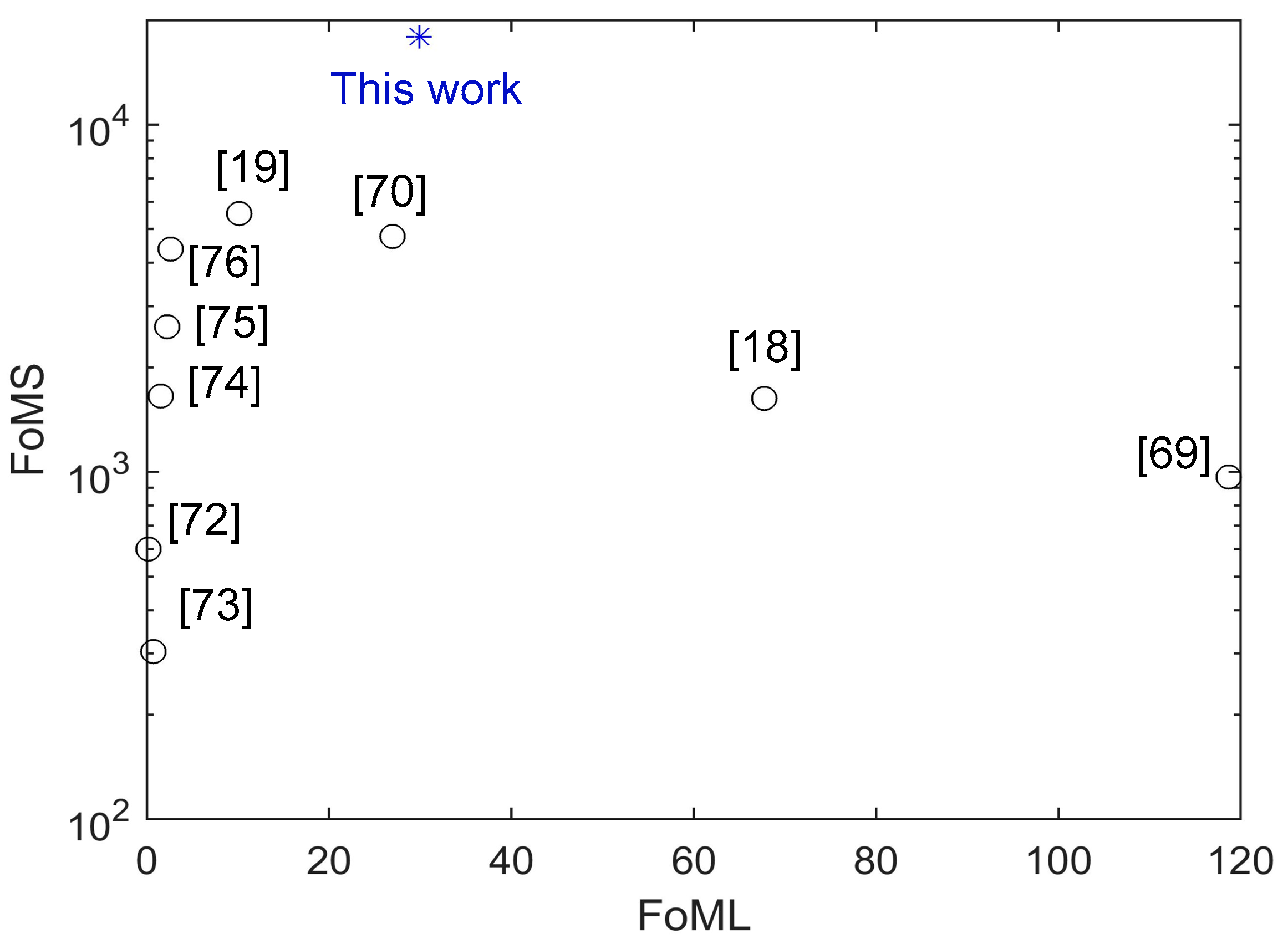
Figure 1. (a) Conventional capacitive coupling. (b) General scheme. (c) Quasi-floating gate transistor.
Applsci 11 03271 g001
Figure 2. Nontunable pseudo-resistors. (a) Single PMOS device. (b) Series topology. (c) Parallel topology.
Applsci 11 03271 g002
Figure 3. Tunable pseudo-resistors. (a) Single voltage-tuned PMOS device. (b) Series voltage-tuned topology. (c) Current-tuned topology.
Applsci 11 03271 g003
Figure 4. Quasi-floating gate (QFG) techniques for amplifier design. (a) QFG input pair. (b) Adaptive bias current source. (c) QFG class AB stage. (d) Dynamic cascode biasing. (e) Class AB current mirror.
Applsci 11 03271 g004
Figure 5. AC-coupled amplifiers. (a) Single-ended input and output. (b) Differential input and single-ended output. (c) Fully differential. (d) Alternative fully differential.
Applsci 11 03271 g005
Figure 6. Single-stage class AB amplifiers. (a) Differential pair amplifier. (b) Telescopic cascode amplifier. (c) Current mirror amplifier. (d) Folded cascode amplifier.
Applsci 11 03271 g006
Figure 7. Two-stage Miller amplifiers. (a) Class A/AB. (b) Class AB/AB.
Applsci 11 03271 g007
Figure 8. Proposed super class AB QFG amplifier. (a) Circuit diagram. (b) Microphotograph (layout image also included, due to the opaque die passivation layer).
Applsci 11 03271 g008aApplsci 11 03271 g008b
Figure 9. Measurement setup.
Applsci 11 03271 g009
Figure 10. Measured transient response to a square input signal.
Applsci 11 03271 g010
Figure 11. Measured total harmonic distortion (THD) versus input amplitude.
Applsci 11 03271 g011
Figure 12. Measured frequency response of the proposed amplifier connected as voltage follower.
Applsci 11 03271 g012
Figure 13. Performance comparison.
Applsci 11 03271 g013
Table 1. Summary of measurement results and performance comparison.
Parameter (units)Figure 8[18][19][69][70][72][73][74][75][76]
CMOS process (nm)13018050050050040180180180130
Supply voltage (V)±0.5±0.9±1±1±11.10.80.71.81.2
Capacitive load (pF)140/120237080700.58202005.2
SR+ (V/μs)5.724.119.810013.212500.141.874.198.7
SR- (V/μs)−7.1−23.33−7.6−78−25.3----−3.8----
DC gain (dB)63.88 a6781.74376.8495157.57275.4
PM (°)61 a846089.575.16560605082.5
GBW (MHz)4.480.574.750.7253.4360057386.5166.1
CMRR @DC (dB)56.7 a73.27868112----19----
PSRR+ @DC (dB)61.5 a44.1725592----52.1----
PSRR- @DC (dB)71.9 a41.87458113----66.4----
Eq. input noise @1MHz (nV/√Hz)27.5--3523023 ----100----
Power (μW)3014.512012010033001.225.411900236.4
Area (mm2)0.0090.0300.0240.0240.0300.0500.0570.0200.070--
FoML (μA/μA)29.9067.7210.15118.6726.950.210.751.542.242.61
FoMS (MHz·pF/mA)179201627.45541.7966.747606003041653.52616.84384.4
F O M A V G = F O M S F O M L 732332237.1338.7358.111.1815.150.576.6106.9
a Simulation results.
Publisher’s Note: MDPI stays neutral with regard to jurisdictional claims in published maps and institutional affiliations.

