Abstract
A novel, inverter-based, fully differential, body-driven, rail-to-rail, input stage topology is proposed in this paper. The input stage exploits a replica bias control loop to set the common mode current and a common mode feed-forward strategy to set its output common mode voltage. This novel cell is used to build an ultralow voltage (ULV), ultralow-power (ULP), two-stage, unbuffered operational amplifier. A dual path compensation strategy is exploited to improve the frequency response of the circuit. The amplifier has been designed in a commercial 130 nm CMOS technology from STMicroelectronics and is able to operate with a nominal supply voltage of 0.3 V and a power consumption as low as 11.4 nW, while showing about 65 dB gain, a gain bandwidth product around 3.6 kHz with a 50 pF load capacitance and a common mode rejection ratio (CMRR) in excess of 60 dB. Transistor-level simulations show that the proposed circuit outperforms most of the state of the art amplifiers in terms of the main figures of merit. The results of extensive parametric and Monte Carlo simulations have demonstrated the robustness of the proposed circuit to PVT and mismatch variations.
1. Introduction
The scaling of CMOS technology, and the diffusion of applications requiring very low power consumption, such as IoT (Internet of Things) nodes [1,2] or biomedical and wearable devices [3,4], have paved the way to the development of compact and ultralow voltage (ULV) circuits. The operation of MOS devices in the deep subthreshold region is mandatory [5,6], to achieve ultralow-power (ULP) consumption and to allow the usage of very low supply voltages.
However, to allow such ultralow supply voltages, specific design approaches are required: floating-gate [7] techniques have been proposed in the past, but the most common solutions are the body-driven (BD) technique and the inverter-based design approach.
Several amplifier designs operating at supply voltages in the order of 0.6 V or lower and exploiting multi-stage, folded cascode or symmetrical OTA topologies have been presented in the last years. The use of a very low supply voltage often requires to eliminate the bias current generator of the differential pair: the resulting pseudo-differential amplifier shows class-AB behavior, but no common mode rejection if the common mode output is exploited. Moreover, there is no control on the bias current, resulting in large variations of small signal performances under process, supply voltage and temperature (PVT) variations.
In BD amplifiers [8,9,10,11,12,13], the body is used as input terminal instead of the gate, thus allowing the input dc level not to be constrained by the threshold voltage of the devices, at the cost of reduced transconductance gain, higher noise, and an input impedance that is not purely capacitive. In this context, Ferreira et al. proposed a Miller amplifier designed in 350 nm CMOS process and operating at a supply voltage of 0.6 V in 2007 [8]. Magnelli et al. published an amplifier with a supply voltage of 0.5 V and 75 nW power consumption in 2014 [10]. In the same year, Ferreira et al. designed an amplifier with a supply voltage as low as 0.25 V [9]. Abdelfattah et al. presented an ULV self-biased amplifier, insensitive to CMOS process variations in 2016 [14]. In 2018 Kulej et al. presented bulk-driven 0.5 V amplifiers, exploiting different gain-boosting techniques in 0.18 µm CMOS process [12]. In 2020 the same authors presented an ULV-ULP class AB amplifier, biased in deep sub-threshold region, that exploits the body-driven non-tailed differential pair [13], attaining state of the art performance in terms of the most important figures of merit.
Inverter-based solutions [15,16,17,18] exploit the CMOS inverter, or inverter-like structures, such as the Arbel cell [19], as building blocks that allow rail-to-rail signal swing with reduced supply voltages. Moreover, in these structures, the elimination of the bias current generator of the differential pair worsens the common mode rejection (CMRR) and results in large variations of small signal parameters under PVT variations.
In this paper, we propose an inverter-based, differential, body-driven input stage, with a replica bias loop that accurately sets the common mode current of the input stage by controlling the gate terminals of the MOS devices. The novel input stage is used to build an ULV, ULP, two-stage amplifier, in which a dual path compensation strategy is exploited to improve the frequency response of the amplifier.
The paper is structured as follows: Section 2 presents the proposed amplifier topology and describes the replica bias loop that sets the common mode current of the inverter based input stage as well as the CMFF technique adopted to improve the CMRR. Section 3 focuses on small signal analysis of dc-gain, CMRR, and frequency response explaining the adopted compensation strategy. Section 4 discusses the design of the amplifier and presents the simulation results and comparisons with ULV, ULP state of the art amplifiers. Finally some conclusions are reported in Section 5.
2. Proposed Topology
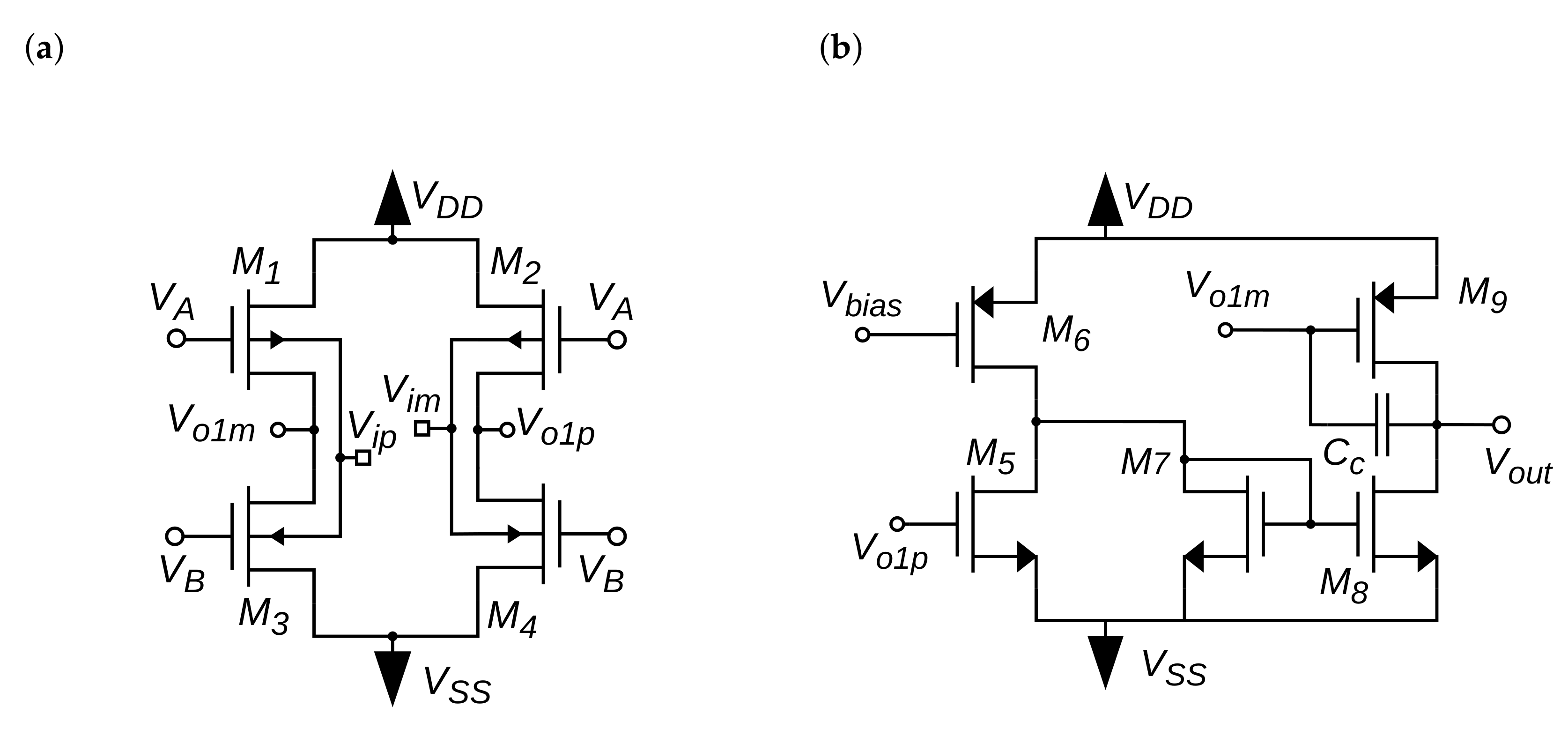
Due to its capability to allow almost rail-to-rail input and output swing, the Arbel cell (or differential inverter) is often used as a building block for low-voltage analog CMOS circuits. To further reduce the minimum supply voltage of the Arbel cell, the bias current generators can be removed and the common mode current can be set by controlling the body terminals of MOS transistors following the approach proposed in [20]. However, for supply voltages lower than 0.5 V, the limited swing of the control voltage at the body terminals reduces the effectiveness of the current setting loop. To overcome this limitation, we propose a body-driven fully differential inverter (Figure 1a) as input stage of the amplifier. We then exploit the gate terminals of the four MOS devices to set both the common mode current by means of a replica bias control loop, and the output common mode voltage through a common mode feed-forward (CMFF) approach. By using the gates as control terminals we are able to enhance the loop gain, thus requiring a smaller swing of the control voltages to guarantee proper operation of the bias control loop even at a very low supply voltage.
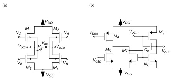
Figure 1.
Schematic of the proposed amplifier: (a) first stage fully differential amplifier; (b) second stage differential to single ended amplifier.
A simple push-pull second stage (Figure 1b) is exploited to convert the differential output of the first stage to a single-ended one, providing further gain to compensate for the reduced gain of the first stage due to the use of the body transconductance. One output of the first stage is directly applied to the gate of the PMOS common-source device, whereas the other one is applied to a NMOS common-source followed by a current mirror, to provide the required dc reversal needed both for the dual path compensation strategy and to improve the CMRR. The bias current of the output stage is given by:
where M is the ratio between the form factor (/) of transistor and the form factor (/) of transistor . is therefore determined by the current source , by the sizing of , and by the current mirror ratio M. This is also the maximum current that can be sinked by the stage, that thus presents a class-A behavior, whereas the maximum sourced current is limited only by the available excursion of the gate voltage of .
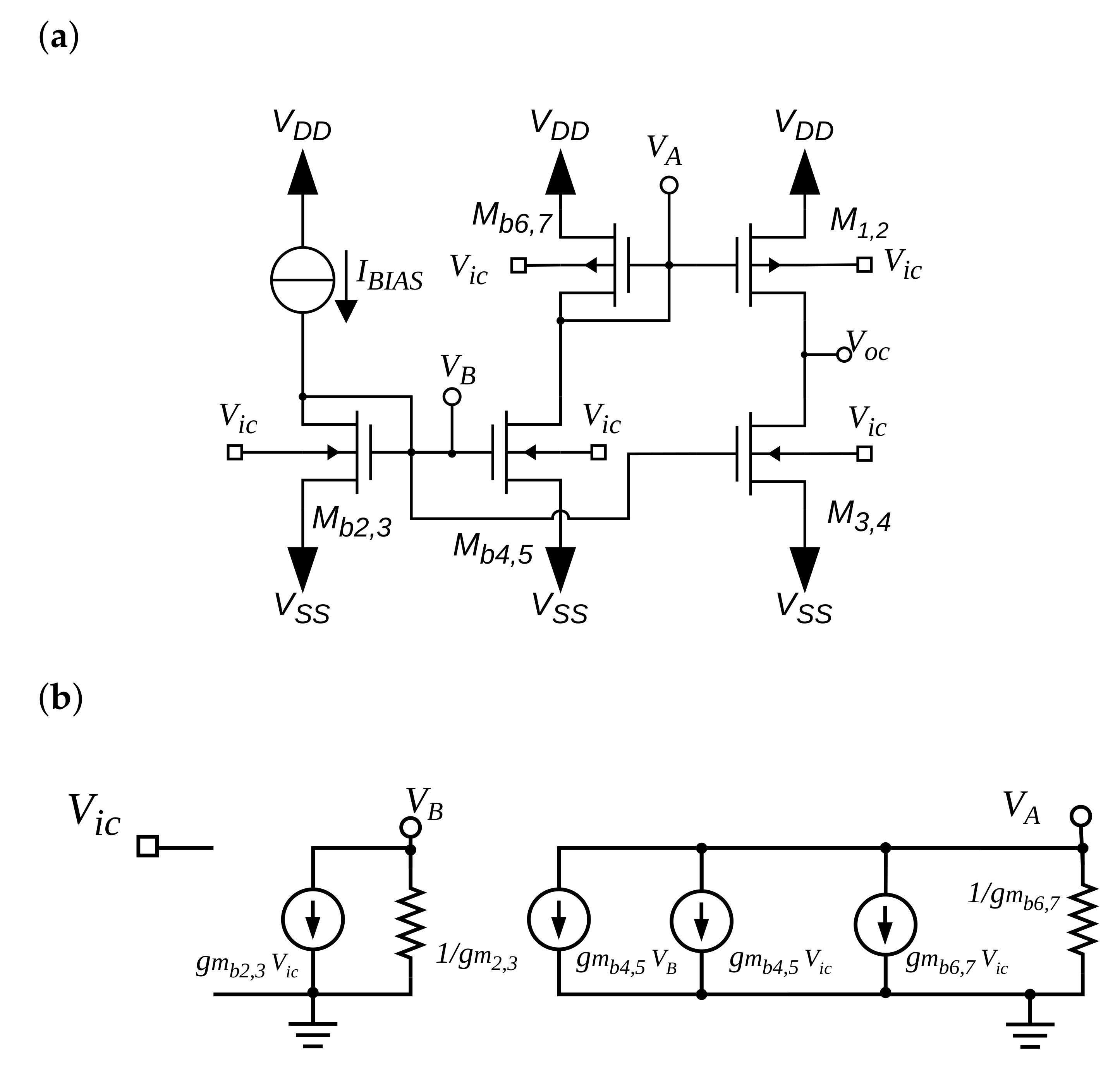
The replica bias loop to set the common mode current of the first stage is shown in Figure 2. The reference current, set by transistor , is applied to devices -, that are a replica of the N-part of the input stage and are diode connected: The loop acts varying the gate voltage to contrast variations of the input common mode and of device parameters. This bias voltage is applied to the gates of the NMOS transistors of the input stage, thus setting its bias current to a scaled replica of the reference current (scaling factor is given by the ratio of the form factors of the devices).
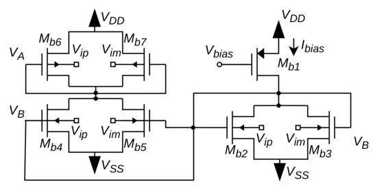
Figure 2.
Schematic of the proposed replica bias circuit to set the common mode current of the input stage.
The gate control voltage is exploited to set the output common voltage of the first stage using a common mode feed-forward (CMFF) technique: In the left part of Figure 2, the reference current is mirrored through devices - and applied to - that are a replica of the P-part of the input stage and are diode connected. The gate voltage is applied to the PMOS transistor of the input stage, thus forming a current mirror, and it can be shown (detailed analysis in the Appendix A) that the output common mode voltage of the first stage is set to . The proposed CMFF does not exploit any reference to set the value of the output common mode voltage of the input stage that is determined by the sizing of the devices. In fact, by looking at Figure 2, it is evident that is equal to (-), and therefore, the output common mode is set close to the analog ground for an appropriate sizing of . For example, assuming a dual supply voltage with = 0.15 V and = −0.15 V, can be set to about 0.15 V in order to have about equal to 0 V which in this example is the analog ground.
3. Small Signal Analysis
In this section, we report the small signal analysis of the proposed amplifier focusing both on the dc performance (in terms of differential gain and CMRR) and ac performance by computing the frequency response and presenting considerations about the compensation strategy.
3.1. DC-Gain and Common Mode Rejection
The replica bias stage contributes to enhance the common mode rejection ratio (CMRR) of the input stage that would otherwise be one (same gain for differential and common mode signals). Denoting with and the input and the output differential voltage of the input stage, respectively, the differential gain can be easily derived referring to the circuit in Figure 1a:
where and are the transconductance and the output conductance of the input stage respectively, , and denote the body transconductance, the gate transconductance and the output conductance of the different MOS transistors, as usual, and the subscripts 1 and 3 refer to PMOS and NMOS devices in Figure 1a, respectively.
Denoting with = (+)/2 and = (+)/2 the input and output common mode voltage of the input stage, respectively, the common mode gain, with the effect of the replica bias control loop, can be derived referring to the common mode equivalent circuit of the input stage shown in Figure 3:
where the approximation holds with the usual assumtpions and . The resulting CMRR can then be calculated as
and is proportional to the intrinsic gain of the devices.
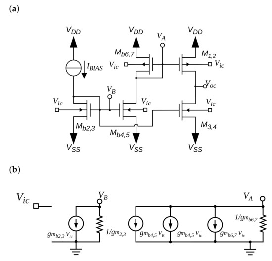
Figure 3.
Common mode equivalent circuit of the input stage with replica bias (a) and corresponding small signal model (b).
The CMRR is further improved by the second stage, since, with the dual path approach, the common mode components at the output of the first stage arrive to the output with opposite phases. The analysis of the circuit in Figure 1b provides:
where and can be expressed as follows:
and
is the output conductance of the second stage.
The overall CMRR is therefore given by
with,
It is clear from (9) that the CMRR can become infinite by choosing:
3.2. Frequency Response and Compensation
The use of a dual signal path in the second stage allows some flexibility in optimizing the frequency response: in particular, the zero provided by the dual path can be exploited to cancel one pole of the overall transfer function thus improving the phase margin.
An approximate analysis of the amplifier can be carried out by exploiting the Miller approximation and referring to the small signal equivalent circuit reported in Figure 4, where and are defined in (2), is given by (7), is the load capacitance and the other capacitances can be expressed as
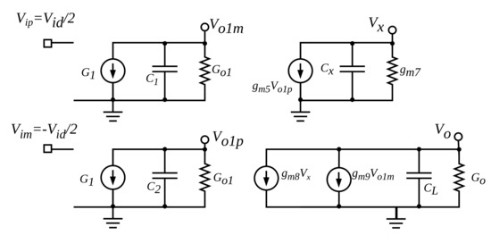
Figure 4.
Simplified small-signal equivalent circuit of the amplifier after applying Miller approximation for frequency response computation.
Since results much larger than , the transfer function has to be calculated by separately considering the paths from = and = to :
The analysis of the circuit in Figure 4 yields a transfer function in the form:
where
is the dc gain, the time constants of the poles are
and
which can be solved by means of well known approximations to obtain the expression of the two zeros as follows:
For large load capacitances , is the dominant pole, and the circuit can be sized to cancel the second pole with one of the zeros, thus improving the phase margin and providing stability without sacrificing the bandwidth. To add a further degree of freedom and achieve an adequate phase margin even for smaller load capacitances, a compensation capacitor can be added between and (i.e., between gate and drain of in Figure 1b): Its pole-splitting effect leads to some reduction of the bandwidth that is however negligible if and moves the pole , placing it nearer to the zero . To evaluate the effect of , we can still exploit the Miller approximation and use the previous results; the capacitance now becomes
and the capacitance has to be substituted by
The expression of the Gain Bandwidth product for the proposed amplifier can be easily derived by combining Equations (16) and (17) as follows:
A simple expression of the negative slew rate can be obtained by noting that, during the discharge of the load capacitor , the amplifier exhibits a class A behaviour with a bias current given by :
During the charge of the load capacitor , the amplifier exhibits a class B behaviour (maximum current is only limited by the voltage swing at the gate of ), and a formula expressing the positive slew rate can be obtained by using the equation for the subthreshold conduction of the MOS transistor [21] as follows:
A theoretical analysis of offset and noise performance of the proposed amplifier is reported in the Appendix A.
4. Amplifier Design and Simulation Results
The proposed amplifier has been designed in a 130 nm CMOS technology from STMicroelectronics featuring a .
4.1. Sizing
All the devices have been biased in the subthreshold region at ||=|| = 150 mV, and a dual supply of ±0.15 V with − = 2|| has been adopted. All the devices in the circuit have been sized with extremely long gates: this choice allows to minimize noise and increase the output resistance and the intrinsic gain of MOS devices as shown in [13]. The bias current of transistors in the input stage has been set to 5 nA as a tradeoff between power consumption and noise performance. For what concerns the second stage, simulations have shown that a design maximizing the CMRR according to (10) is very sensitive not only to mismatches but also to PVT variations; the stage has thus been optimized to provide good CMRR performance in the different PVT conditions by means of a design centering approach.
To minimize power consumption, a 4 nA bias current has been adopted for the second stage. Even if this current is lower than the bias current of the first stage, the amplifier can still be efficiently compensated because the body driven input stage has a much lower transconductance than the second stage. A load capacitance of 50 pF has been assumed and a compensation capacitor of 1.2 pF has been added to provide an adequate phase margin. Table 1 reports sizing, bias current, and small signal parameters for all the devices.

Table 1.
Nominal transconductance, sizing and output resistance of transistors.
4.2. Simulation Results
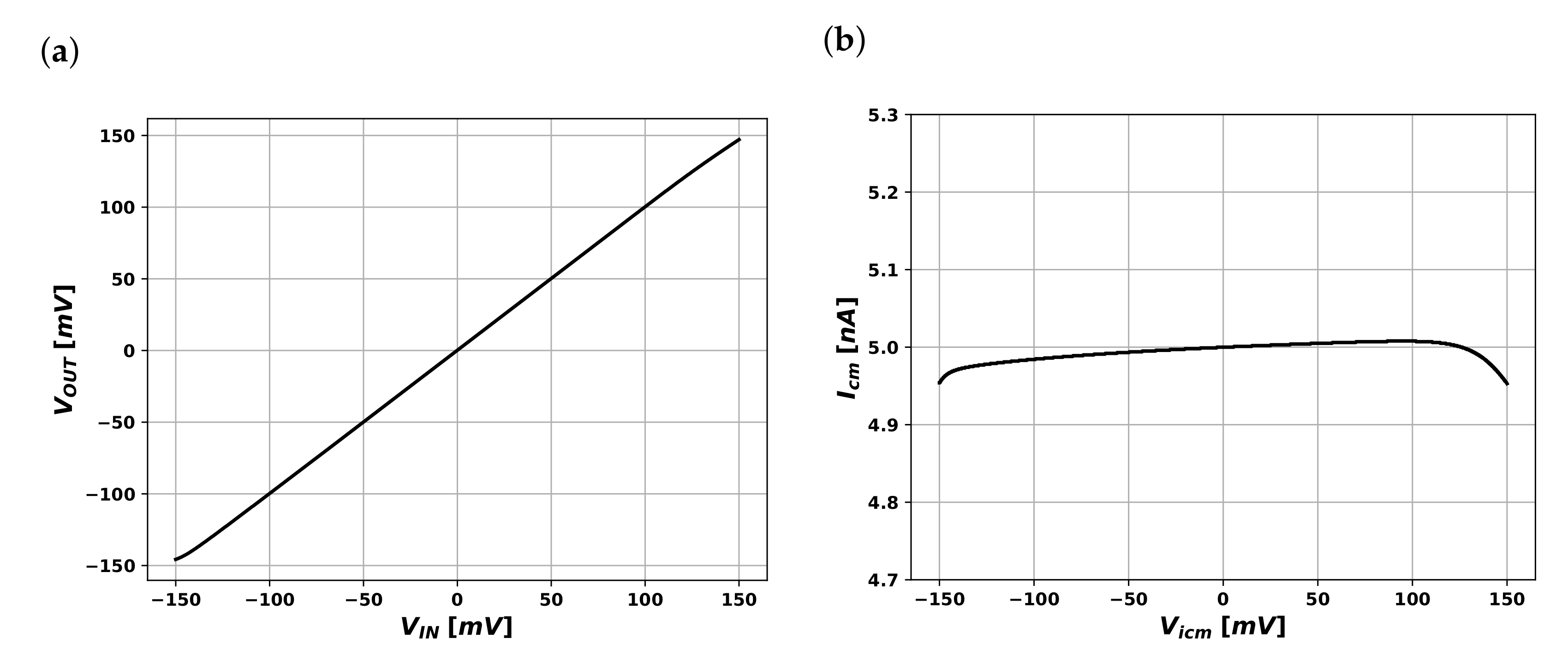
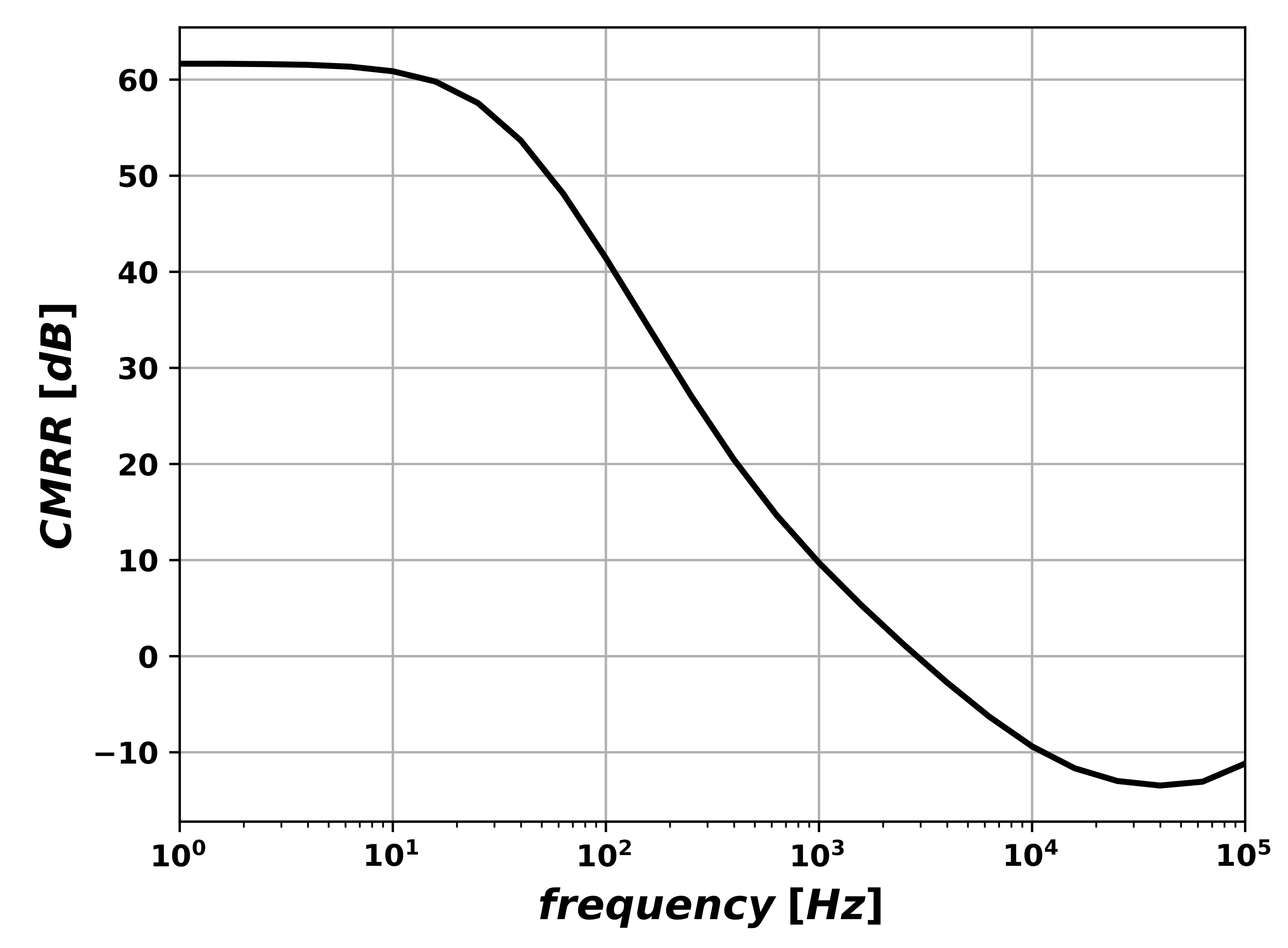
The circuit has been simulated in the Cadence Virtuoso environment to test both open-loop and closed-loop performance. Figure 5 reports the magnitude and phase of the open-loop differential gain: a 64.6 dB dc gain with a 3.58 kHz unity gain frequency and a phase margin of about 54° are achieved in typical conditions. The amplifier has been simulated in a unity-gain buffer configuration to test closed-loop performance. Figure 6a shows the dc input-output characteristic of the buffer, highlighting a rail-to-rail output swing. The bias control loop is able to keep the common mode current of the input stage constant under input common mode variations, as shown in Figure 6b, thus improving common mode rejection and linearity. The CMRR is approximately 61 dB as shown in Figure 7. Supply rejection is around 27 dB, and the amplifier power dissipation is only 11.4 nW.
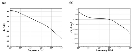
Figure 5.
Open-loop differential gain frequency response: magnitude (a) and phase (b).
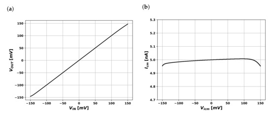
Figure 6.
DC transfer charachterisitc (a) and DC bias current of the input stage vs. input common mode voltage (b).
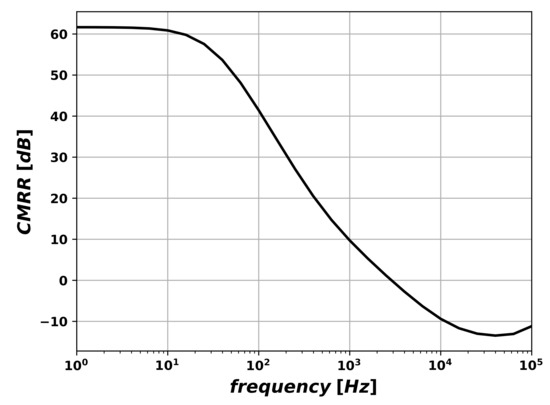
Figure 7.
Magnitude of common mode rejection ratio (CMRR).
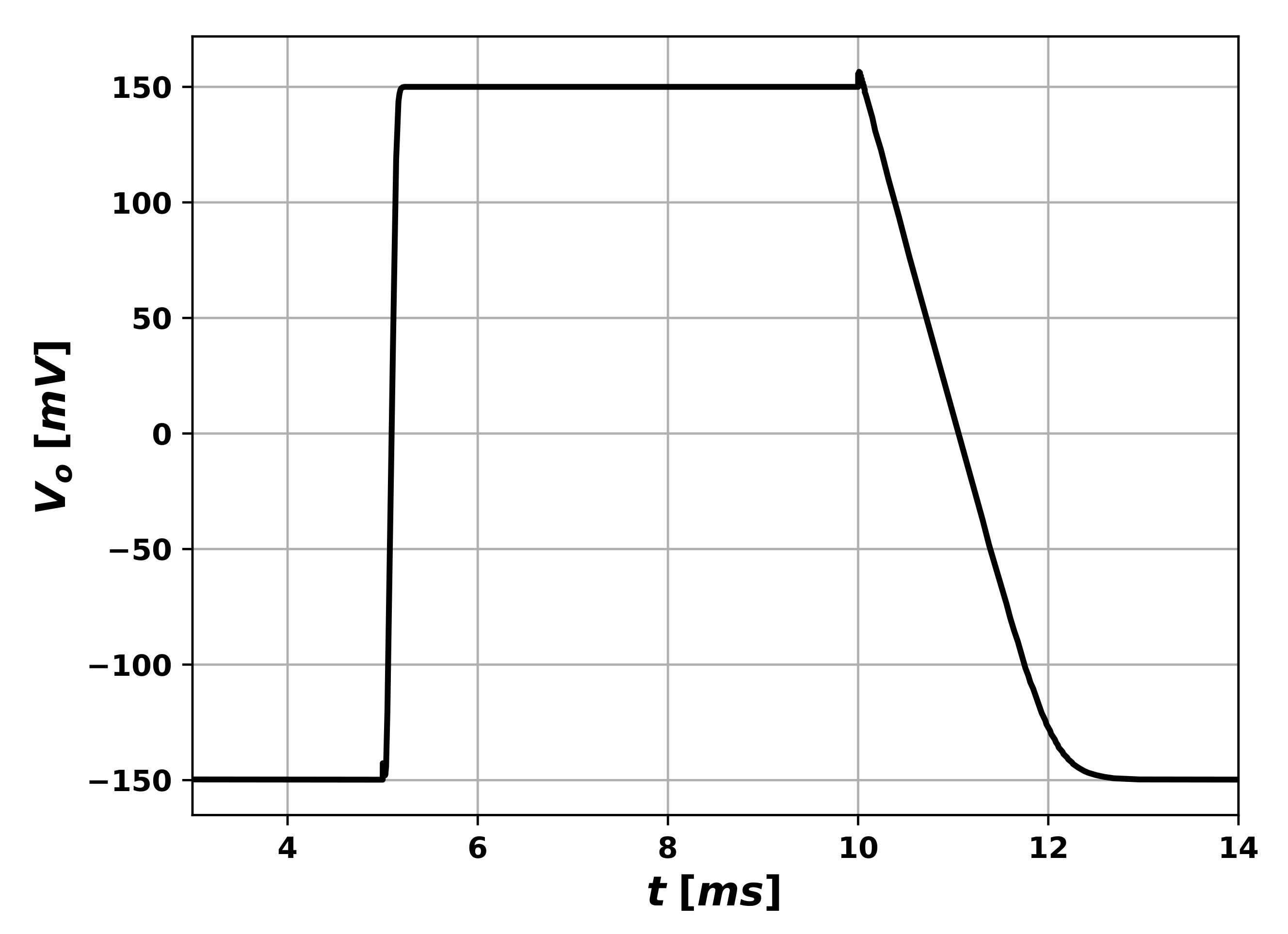
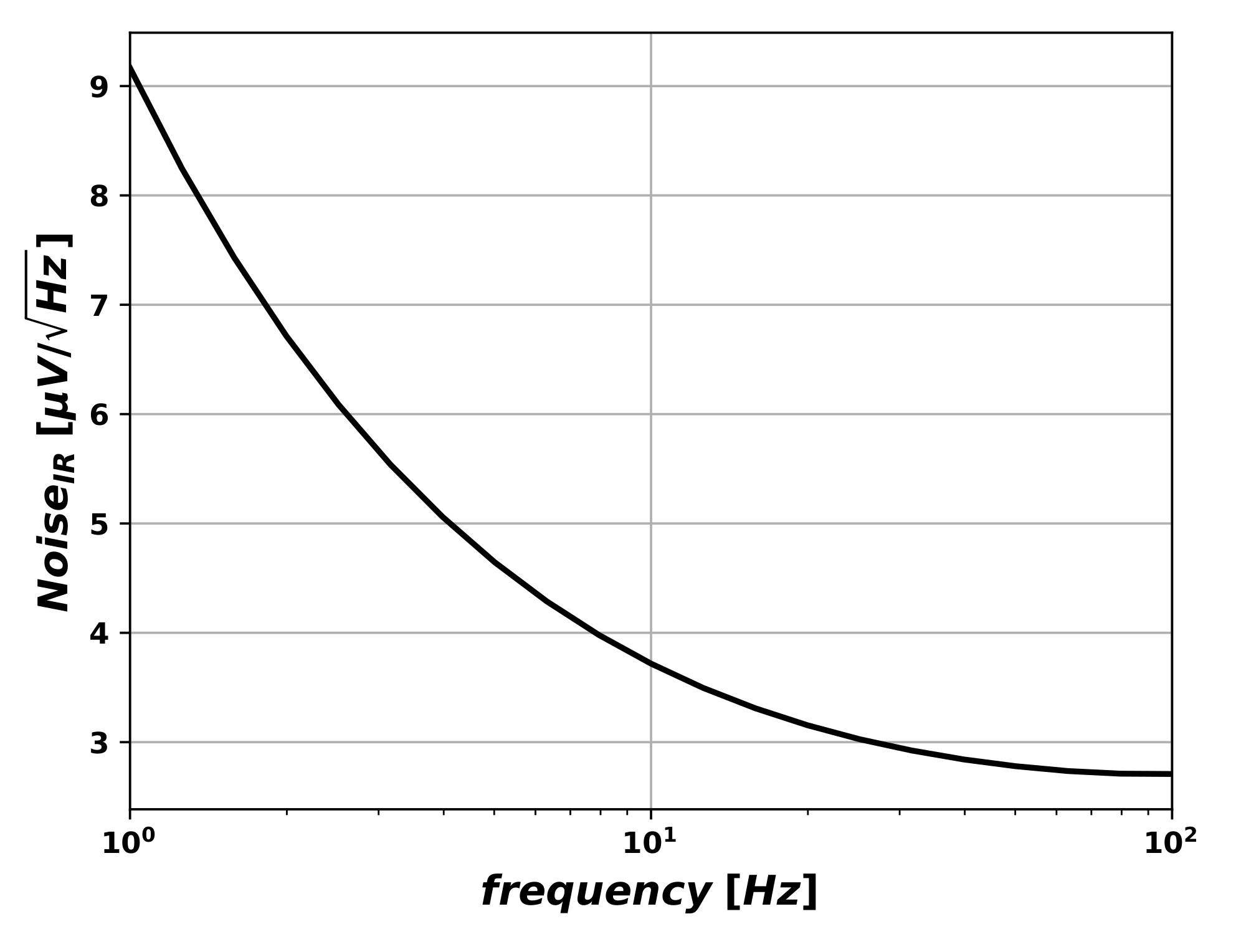
The slew rate has been evaluated simulating the response to a full swing (300 ) input step, shown in Figure 8: The positive slew rate is 1.7 V/ms, whereas a much lower negative slew rate of 0.14 V/ms is achieved, limited by the current source . Total harmonic distortion (THD) for a 300 input signal at 10 Hz is 0.84%. To give more detailed informations about linearity performance, the THD versus the peak-to-peak input voltage is shown In Figure 9a, whereas the differential voltage gain (in dB) as a function of the input common mode voltage is reported in Figure 9b to demonstrate the almost rail to rail input voltage range of the proposed amplifier. Finally the equivalent input referred noise is depicted in Figure 10 showing a spot noise at 100 Hz of about 2.69 .

Figure 8.
Response to a full swing input step.
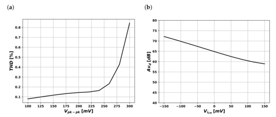
Figure 9.
Total harmonic distortion (THD) vs. input signal amplitude (a) and differential gain vs. input common mode voltage (b).

Figure 10.
Equivalent input noise.
An area footprint of the amplifier of about 0.0064 mm has been estimanted by using the Cadence Layout XL tool.
To assess the robustness of the proposed design, PVT and Monte-Carlo simulations have been carried out. Table 2 reports the simulated performance under different process corners, highlighting a very good stability of the amplifier performance. The amplifier’s robustness has been tested also under supply voltage and temperature variations. Main amplifier parameters under supply voltage variations from 0.24 to 0.36 V are reported in Table 3, whereas simulation results under temperature variations in the range from −10 °C to 110 °C are shown in Table 4.

Table 2.
Amplifier performance for different process corners.

Table 3.
Amplifier performance vs. supply voltage −.

Table 4.
Amplifier performance vs. temperature.
Monte-Carlo simulations have been performed to evaluate the effect of mismatches; Table 5 reports mean values and standard deviations of the main performance parameters for a 200-run Monte-Carlo mismatch simulation, highlighting a good stability.

Table 5.
Monte Carlo simulations.
4.3. Results and Comparision
Table 6 compares the simulated performance of the proposed amplifier with other ULV, ULP implementations from the literature. In order to compare the performance of several different designs, we have considered the usually adopted four figures of merit (FOMs) defined as follows:
where the large signal has been computed both referring to the average slew rate and to the worst case one (). The comparison in Table 6 shows the effectiveness of the proposed approach: Extremely high values of the small signal FOMs ( and ) are achieved. is particularly high thanks to the adoption of an extremely low supply voltage. This result is due to the combination of an Arbel-type approach, that doubles the gain of the first stage and thus the GBW product, and a dual-path second stage that allows achieving stability without sacrificing the bandwidth. Similar values of the small signal FOMs are obtained only by [22], that however uses a higher supply voltage, resulting in a lower , and [18]. This latter however is a single-stage amplifier with limited input common mode range and which provides a much lower gain, and is biased at an extremely low current; no additional circuit is used to stabilize the dc current, that therefore presents large variations in PVT conditions. The proposed amplifier has not been optimized for large signal performance, and the negative slew rate is limited by the bias current set by resulting in a limited value for the worst case large signal . If we consider the average slew rate for the computation of the large signal , the obtained values are comparable with state-of-the-art class-A amplifiers. Much better is achieved only by [12,13] that present a class-AB behavior.

Table 6.
Comparison with ultralow voltage (ULV) state of the art amplifiers.
5. Conclusions
In this paper, we have proposed an ultralow voltage Amplifier operating at 0.3 V supply voltage. The Arbel (differential inverter) approach and a dual-path differential-to-single-ended second stage are exploited to achieve 64.6 dB gain with high CMRR and an extremely high efficiency, resulting in an unity-gain frequency of about 3.6 kHz for a 50 pF load with a power consumption of only 11.4 nW. A replica-based bias control loop and a common-mode feed-forward approach are exploited to set the bias current and the output common mode voltage of the input stage, thus allowing a high robustness against PVT and mismatch variations. Comparison against the state of the art has shown that the proposed amplifier outperforms all the previously published Amplifiers in terms of the small signal figures of merit, while guaranteeing a very good tradeoff between noise, power consumption, area footprint, gain and CMRR.
Author Contributions
Conceptualization, R.D.S.; methodology, F.C., R.D.S. and G.S.; software, R.D.S. validation, F.C., R.D.S. and G.S., A.T.; formal analysis, F.C.; investigation, F.C., R.D.S. and G.S.; resources, A.T.; writing—original draft preparation, R.D.S.; writing—review and editing, F.C., G.S. and A.T.; supervision G.S.; funding acquisition, A.T. All authors have read and agreed to the published version of the manuscript.
Funding
This research received no external funding.
Institutional Review Board Statement
Not applicable.
Informed Consent Statement
Not applicable.
Conflicts of Interest
The authors declare no conflict of interest.
Appendix A
Appendix A.1. CMFF Analysis
The circuit can be analyzed with reference to Figure 3 and exploiting the equation for the subthreshold conduction of the MOS transistor [21]:
where
is the thermal voltage. We assume balanced supply voltage , and no input common mode signal, so that .
The analysis of the leftmost branch of the circuit provides
Let the current flowing in : an expression for similar to (A3) can be written, but now . By exploiting Taylor expansion, the ratio between and can now be expressed as
The voltage is set by , since it results
and are applied to the gates of and , respectively; the currents of and can be derived by exploiting the same approximation in (A4) as
By imposing we obtain .
Appendix A.2. Offset Analysis
The random offset of the proposed amplifier is mostly due to the mismatches of the devices in the input stage. The sub-threshold current equation can be rewritten as
where
and the effect of the drain-source voltage is neglected. We can assume the difference in the threshold voltages (hence in the overdrive voltages) as the main source of mismatch [13]. Considering the pair of NMOS (PMOS) devices, their overdrive voltages can be written as
where x = n,p. Under the hypothesys of infinite CMRR (given by (10)), The input offset voltage can be calculated as the differential output voltage due to the overdrive mismatch divided by Ad1; since mismatches for NMOS and PMOS devices are uncorrelated, we get
Appendix A.3. Noise Analysis
We can assume that the main noise contributors are the channel noise currents of the devices in the input pair; noise in the second stage can be neglected, thanks to the gain of the first stage, and noise in the biasing circuit does not affect the output under the hypothesys of infinite CMRR. Noise sources in the MOS devices M1–M4 are uncorrelated, thus the equivalent input noise spectrum can be written as
(we have exploited (10) to simplify the expression). The noise spectral density for each transistor can be written as
where
is the thermal noise contribution and
is the flicker noise. Substituting (A14) and (A15) into (A13) we get
References
- Harpe, P.; Gao, H.; Van Dommele, R.; Cantatore, E.; Van Roermund, A.H.M. A 0.20 mm2 3 nW signal acquisition IC for miniature sensor nodes in 65 nm CMOS. IEEE J. Solid State Circuits 2016, 51, 240–248. [Google Scholar] [CrossRef]
- Toledo, P.; Crovetti, P.; Klimach, H.; Bampi, S. A 300-mV supply, 2 nW-power, 80 pF-load CMOS digital-based OTA for IoT interfaces. In Proceedings of the 2019 International Conference on Electronics, Circuits and Systems (ICECS), Genova, Italy, 27–29 November 2019; pp. 170–173. [Google Scholar]
- Della Sala, R.; Monsurrò, P.; Scotti, G.; Trifiletti, A. Area-efficient low-power bandpass Gm-C filter for epileptic seizure detection in 130 nm CMOS. In Proceedings of the 2019 International Conference on Electronics, Circuits and Systems (ICECS), Genova, Italy, 27–29 November 2019; pp. 298–301. [Google Scholar]
- Liu, Z.; Tan, Y.; Li, H.; Jiang, H.; Liu, J.; Liao, H. A 0.5-V 3.69-nW complementary source-follower-C based low-pass filter for wearable biomedical applications. IEEE Trans. Circuits Syst. I Regul. Pap. 2020, 67, 4370–4381. [Google Scholar] [CrossRef]
- Grasso, A.D.; Marano, D.; Palumbo, G.; Pennisi, S. Design methodology of subthreshold three-stage CMOS OTAs suitable for ultra-low-power low-area and high driving capability. IEEE Trans. Circuits Syst. I Regul. Pap. 2015, 62, 1453–1462. [Google Scholar] [CrossRef]
- Centurelli, F.; Fava, A.; Olivieri, M.; Tommasino, P.; Trifiletti, A. A low-voltage class-AB OTA exploiting adaptive biasing. Int. J. Electron. Commun. (AEU) 2020, 122, 153282. [Google Scholar] [CrossRef]
- Algueta Miguel, J.M.; Lopez-Martin, A.J.; Acosta, L.; Ramirez-Angulo, J.; Gonzalez Carvajal, R. Using floating gate and quasi floating-gate techniques for rail-to-rail tunable CMOS transconductor design. IEEE Trans. Circuits Syst. I Regul. Pap. 2011, 58, 1604–1614. [Google Scholar] [CrossRef]
- Ferreira, L.H.C.; Pimenta, T.C.; Moreno, L.R. An ultra-low-voltage ultra-low-power CMOS Miller OTA with rail-to-rail input/output swing. IEEE Trans. Circuits Syst. II Express Briefs 2007, 54, 843–847. [Google Scholar] [CrossRef]
- Ferreira, L.H.C.; Sonkusale, S.R. A 60-dB gain OTA operating at 0.25-V power supply in 130-nm digital CMOS process. IEEE Trans. Circuits Syst. I Regul. Pap. 2014, 61, 1609–1617. [Google Scholar] [CrossRef]
- Magnelli, L.; Amoroso, F.A.; Crupi, F.; Cappuccino, G.; Iannaccone, G. Design of a 75-nW, 0.5-V subthreshold complementary metal-oxide-semiconductor operational amplifier. Int. J. Circuit Theory Appl. 2014, 42, 967–977. [Google Scholar] [CrossRef]
- Cabrera-Bernal, E.; Pennisi, S.; Grasso, A.D.; Torralba, A.; Gonzalez Carvajal, R. 0.7-V three-stage class-AB CMOS operational transconductance amplifier. IEEE Trans. Circuits Syst. I Regul. Pap. 2016, 63, 1807–1815. [Google Scholar] [CrossRef]
- Kulej, T.; Khateb, F. Design and implementation of sub 0.5-V OTAs in 0.18-µm CMOS. Int. J. Circuit Theory Appl. 2018, 46, 1129–1143. [Google Scholar] [CrossRef]
- Kulej, T.; Khateb, F. A compact 0.3-V class AB bulk-driven OTA. IEEE Trans. Very Large Scale Integr. (VLSI) Syst. 2020, 28, 224–232. [Google Scholar] [CrossRef]
- Abdelfattah, O.; Roberts, G.W.; Shih, I.; Shih, Y.-C. An ultra-low-voltage CMOS process-insensitive self-biased OTA with rail-to-rail input range. IEEE Trans. Circuits Syst. I Regul. Pap. 2015, 62, 2380–2390. [Google Scholar] [CrossRef]
- Ruscio, D.; Centurelli, F.; Monsurrò, P.; Trifiletti, A. Reconfigurable low voltage inverter-based sample-and-hold amplifier. In Proceedings of the 2017 Conference on Ph.D. Research in Microelectronics and Electronics (PRIME), Giardini Naxos, Taormina, Italy, 12–15 June 2017; pp. 133–136. [Google Scholar]
- Braga, R.A.S.; Ferreira, L.H.C.; Coletta, G.D.; Dutra, O.O. A 0.25-V calibration-less inverter-based OTA for low-frequency Gm-C applications. Microelectron. J. 2019, 83, 62–72. [Google Scholar] [CrossRef]
- Baghtash, H.F. A 0.4 V, tail-less, fully differential trans-conductance amplifier: An all-inverter-based stracture. Analog Integr. Circuits Signal Process. 2020, 104, 1–15. [Google Scholar] [CrossRef]
- Rodavalho, L.H.; Aiello, O.; Ramos Rodriguez, A. Ultra-low-voltage inverter-based operational transconductance amplifiers with voltage gain enhancement by improved composite transistors. MDPI Electron. 2020, 9, 1410. [Google Scholar] [CrossRef]
- Arbel, A.F.; Goldminz, L. Output stage for current-mode feedback amplifiers, theory and applications. Analog Integr. Circuits Signal Process. 1992, 2, 234–255. [Google Scholar] [CrossRef]
- Grasso, A.D.; Pennisi, S.; Scotti, G.; Trifiletti, A. 0.9-V Class-AB Miller OTA in 0.35- m CMOS with Threshold-Lowered Non-Tailed Differential Pair. IEEE Trans. Circuits Syst. I Regul. Pap. 2017, 64, 1740–1747. [Google Scholar] [CrossRef]
- Fjeldly, T.A.; Shur, M. Threshold voltage modeling and subthreshold regime of operation of short-channel MOSFET’s. IEEE Trans. Electron Devices 1993, 40, 137–145. [Google Scholar] [CrossRef]
- Deo, N.; Sharan, T.; Dubey, T. Subthreshold biased enhanced bulk-driven double recycling current mirror OTA. Analog Integrated Circuits and Signal Processing. Analog Integr. Circuits Signal Process. 2020, 105, 229–242. [Google Scholar] [CrossRef]
- Centurelli, F.; Monsurrò, P.; Parisi, G.; Tommasino, P.; Trifiletti, A. A 0.6 V class-AB rail-to-rail CMOS OTA exploiting threshold lowering. IET Electron. Lett. 2018, 54, 930–931. [Google Scholar] [CrossRef]
Publisher’s Note: MDPI stays neutral with regard to jurisdictional claims in published maps and institutional affiliations. |
© 2021 by the authors. Licensee MDPI, Basel, Switzerland. This article is an open access article distributed under the terms and conditions of the Creative Commons Attribution (CC BY) license (http://creativecommons.org/licenses/by/4.0/).

