Article

Design Techniques for Low-Voltage RF/mm-Wave Circuits in Nanometer CMOS Technologies

Dipartimento di Ingegneria Elettrica Elettronica e Informatica (DIEEI), University of Catania, 95125 Catania, Italy
Appl. Sci. 2022, 12(4), 2103; https://doi.org/10.3390/app12042103
Submission received: 7 January 2022 / Revised: 12 February 2022 / Accepted: 14 February 2022 / Published: 17 February 2022

Abstract

:
This paper reviews state-of-the-art design approaches for low-voltage radio frequency (RF) and millimeter-wave (mm-wave) CMOS circuits. Effective design techniques at RF/mm-wave frequencies are described, including body biasing in fully depleted (FD) silicon-on-insulator (SOI) CMOS technologies and circuit topologies based on integrated reactive components (i.e., capacitors, inductors and transformers). The application of low-voltage design techniques is discussed for the main RF/mm-wave circuit blocks, i.e., low-noise amplifiers (LNAs), mixers and power amplifiers (PAs), highlighting the main design tradeoffs.

1. Introduction

The success and pervasiveness of CMOS integrated circuits (ICs) have been mainly due to the continuous technology scaling that has improved transistor performance, even at RF and mm-wave operations, along with the lower production costs to comply with the mass market requirements. Thanks to this extreme scaling, advanced nanometer CMOS technologies are now suited to a wide range of applications up to 100 GHz (e.g., 5G, automotive radar, and imaging), with significant advantages over traditional compound semiconductor or heterojunction bipolar transistors (HBT), in terms of the level of integration, thus allowing complex system-on-chip (SoC) implementations [1]. Furthermore, CMOS scaling produces a continuous decrease in the supply voltage (well below 1 V), enabling new applications, such as wireless sensor networks (WSNs) and the Internet of Things (IoTs). Unfortunately, sub 1-V supply voltages involve the circuit design, especially at RF/mm-wave frequencies, thus requiring nonstandard circuit topologies and proper techniques to mitigate the voltage limitations. This work presents the most interesting approaches to comply with very low supply voltages for RF/mm-wave circuits, with a particular focus on nanometer CMOS technologies. A crucial role in RF/mm-wave, low-voltage operation is performed by the reactive components, especially inductive components (i.e., integrated inductors and transformers) that can be properly exploited to compensate for the limited voltage headroom. Another important contribution is also given by the body biasing approach, especially in fully depleted (FD) silicon-on-insulator (SOI) platforms [2], which further improves IC performance at low-voltage supply levels.
This paper is organized as follows: Section 2 reviews the main features, limitations, and design issues of inductive components (i.e., spiral inductors and transformers), with reference to the back-end-of-line (BEOL) in CMOS. Section 3 is dedicated to the body biasing approach in both traditional bulk and FD-SOI technologies. Low-voltage circuit topologies for RF/mm-wave operation are revised in Section 4, with special insights into low-noise amplifiers (LNAs), mixers and power amplifiers (PAs). Finally, Section 5 draws the main conclusions, highlighting future challenges for low-voltage RF/mm-wave ICs.

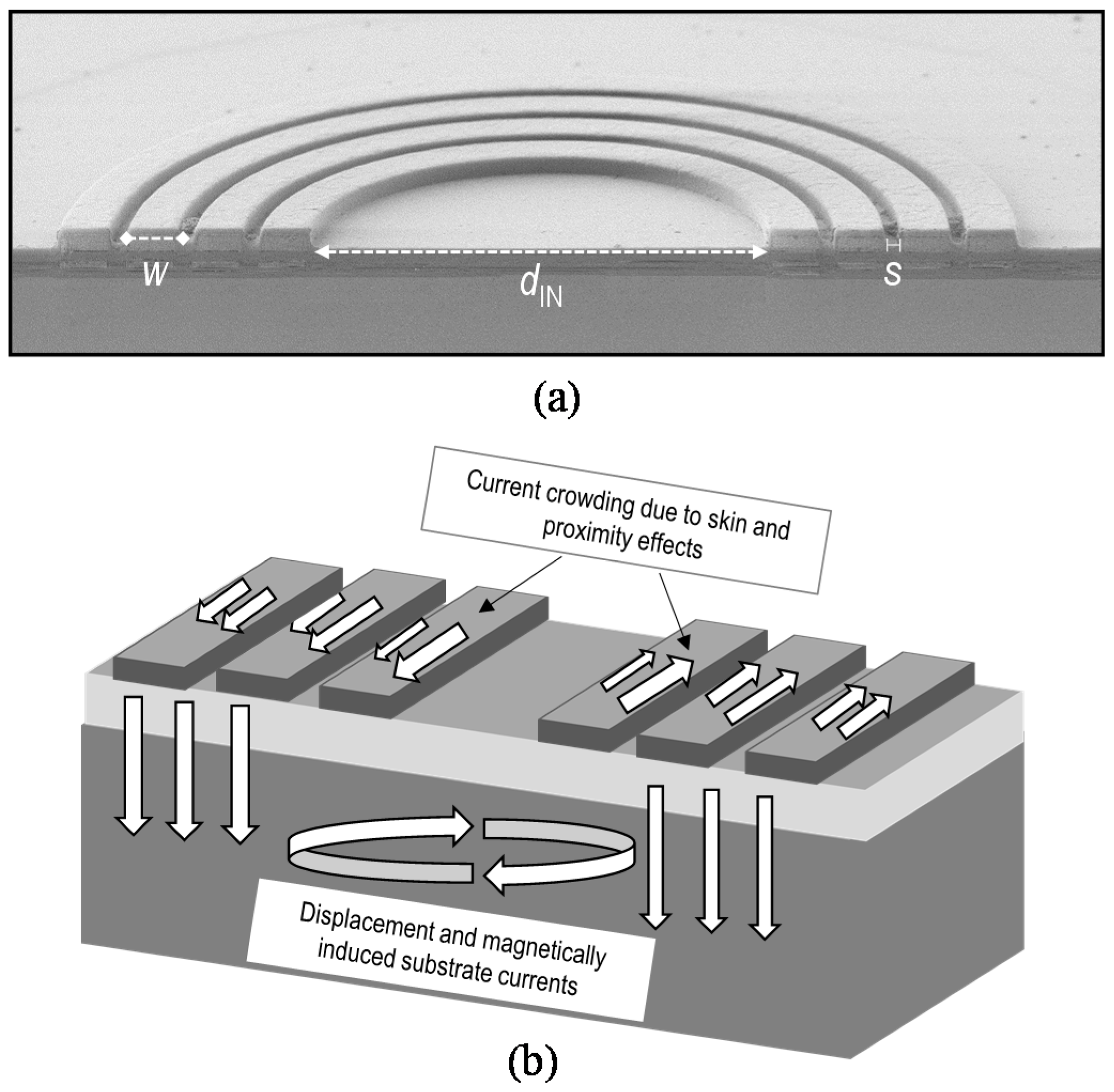
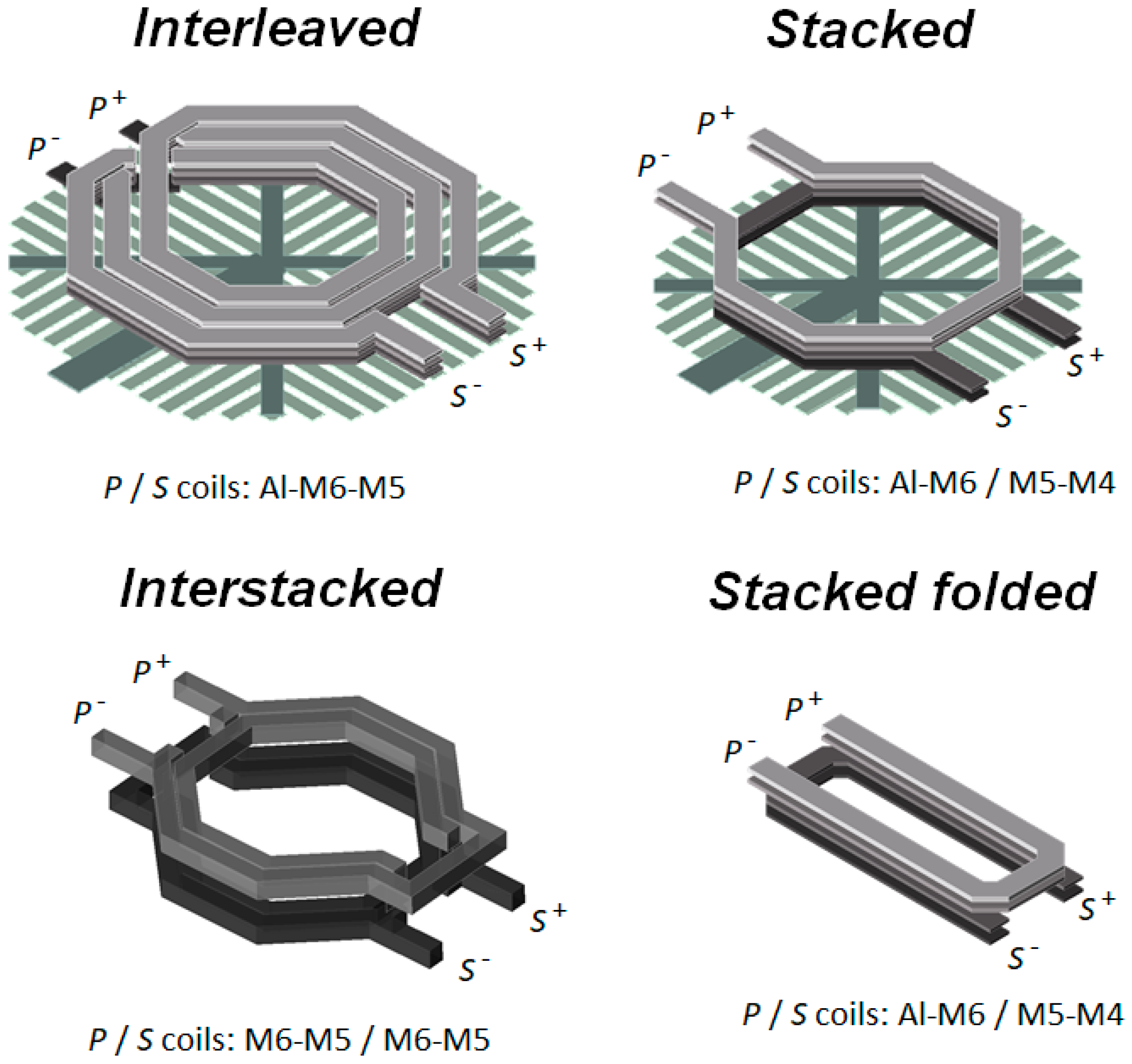
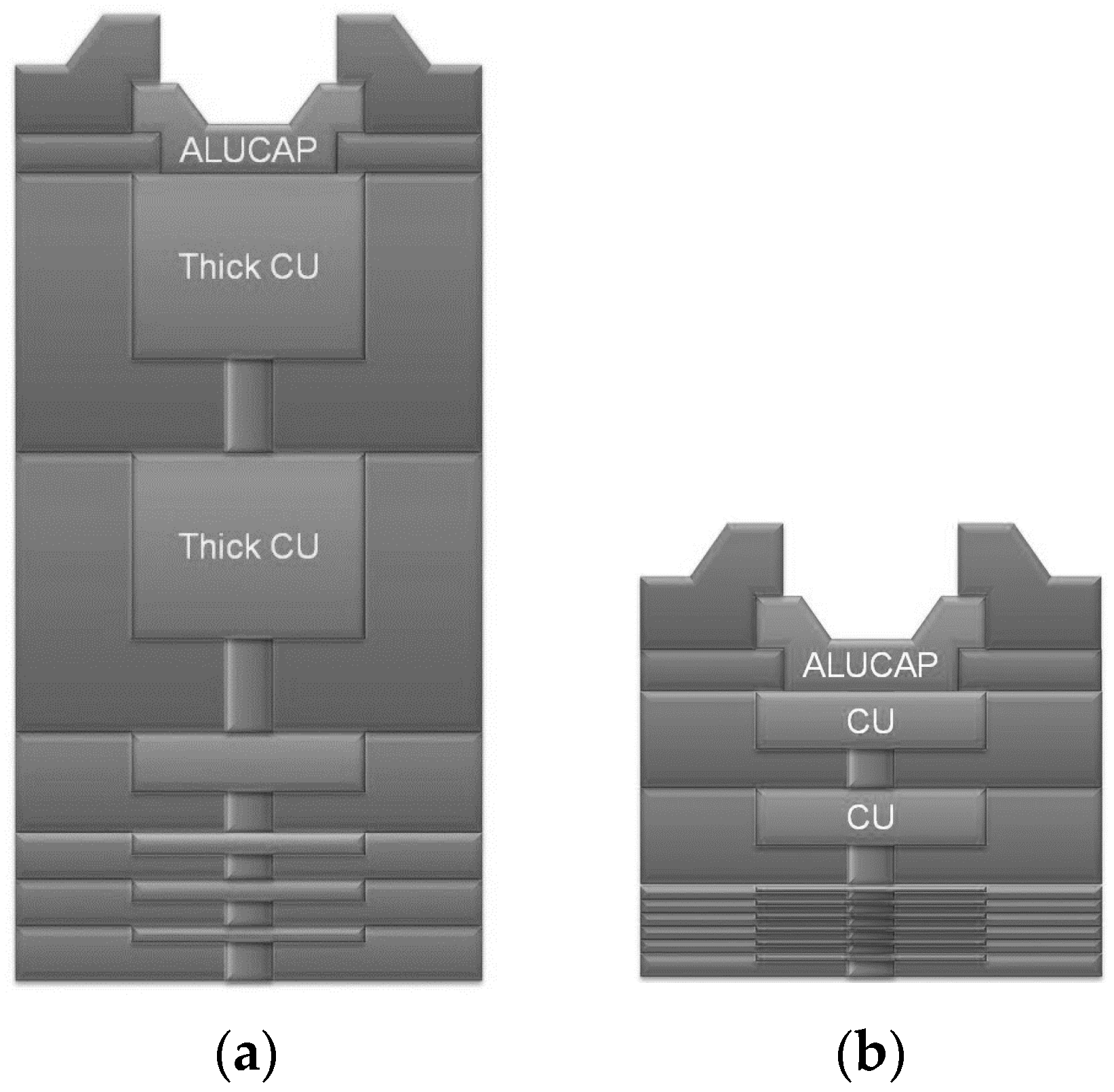
2. Integrated Inductive Components: Loss Phenomena and Main Design Guidelines

Inductive components are very important in RF/mm-wave integrated circuits (ICs). Indeed, they are exploited to implement irreplaceable functionality, such as simultaneous impedance/noise matching to the 50-ohm input source in LNAs, impedance matching and tuned resonant loads in amplifiers, LC tank in voltage-controlled oscillators, and integrated single-ended-to-differential conversion [3,4,5,6,7]. The Q-factor maximization at a given value of inductance, L, is the most common design issue. Other important figures of merit are the inductor ωQL product, the transformer characteristic resistance (TCR) and the insertion loss (IL) [8,9].
A scanning electron microscope (SEM) cross-section of a silicon-integrated spiral inductor is shown in Figure 1a. Geometrical parameters (i.e., layout parameters) can be properly tuned within the technology constraints, namely, the coil shape (i.e., circular, polygonal or squared), the number of turns, n, the inner diameter, dIN, the metal width, w, and the metal spacing, s. The process parameters, such as the metal BEOL, the thickness and permittivity of the insulation layers, and the substrate conductivity, cannot be modified. Generally, the design of inductive devices is aimed at minimizing energy loss. The main energy dissipation phenomena of silicon-integrated inductive components are shown in Figure 1b. They occur in the metal layers that form the coil (series losses), as well as in the conductive layers below (parallel losses). The former is mainly due to the current crowding on the internal sides of the coil, due to skin and proximity effects. Current crowding rises with an increase in the operating frequency, thus increasing the equivalent resistance of the inductor. Thick conductive metals and multi-layer structures are common arrangements to lower the series losses, but their effectiveness degrades at RF/mm-wave frequencies. According to Faraday’s law, current crowding is stronger in the inner turns. Therefore, the adoption of spirals with a low fill ratio, ρ, is a common rule [10].
Figure 1b also depicts two different mechanisms taking place in the substrate layers, i.e., the (vertical) displacement currents and the (horizontal) magnetically induced currents. Both electrically and magnetically induced currents increase at RF/mm-wave frequencies and dominate the inductor losses. Substrate shielding can be implemented to reduce the effect of parallel losses for RF operation [11,12].
The design of an inductive component starts with its geometrical parameters, which set the low-frequency inductance, LDC. The inductance maximum value reduces with an increase in the operating frequency, due to self-resonance. Actual inductors have a typical inductance range from a few hundred picohenrys to tens of picohenrys, moving from tens of gigahertz to 100 GHz and beyond. Since inductance is mainly dependent on n, the inner diameter, dIN, is adjusted to trade off the silicon area with current crowding phenomena, by using a low fill ratio, ρ, while the metal width, w, is typically tuned to set the peak quality factor, QMAX, at the operating frequency. The metal spacing, s, must be set at the minimum value to maximize the coil auto-inductance. For the purpose of completeness, Table 1 summarizes the relationship between the electrical performance and the layout/process parameters of an integrated inductor.
A special role in RF/mm-wave ICs is performed by transformers [13]. Figure 2 shows the main structures of integrated transformers. The traditional arrangements are the interleaved and stacked configurations. The interleaved configuration guarantees better winding Q-factors at the cost of a lower magnetic coupling factor, k, compared to the stacked configuration. However, interleaved transformers easily implement high transformer ratios, N, and achieve better SRFs. The interstacked configuration exploits mixed interleaved/stacked coils and guarantees higher k with respect to the stacked configuration, providing full winding symmetry [6,14,15]. Finally, when the operative frequency is excessively high with respect to the adopted BEOL, stacked folded configurations can be exploited [16]. Table 2 summarizes the pros and cons of the integrated transformer structures shown in Figure 2.
A final comment must be made about the BEOL of integration technologies. Bipolar and BiCMOS technologies benefit from optimized BEOL for RF/mm-wave applications with at least two thick copper top metals (i.e., thicker than 2 μm), along with thick intermetal oxide layers to reduce losses and capacitive parasitics. On the other hand, CMOS technologies usually adopt a standard BEOL with thin metals and intermetal oxides, leading to lower quality passive devices with limited SRF. Figure 3 shows a comparison between an optimized BiCMOS process [17] and a 28-nm CMOS technology with standard BEOL [2]. Although at mm-wave frequencies, an optimized BEOL technology produces small performance enhancements, due to increased fringing effects [18], it could have a significant impact on inductive components operated at lower frequencies, where higher inductances and, hence, larger coils are used. Therefore, inductor design in standard CMOS is still a challenging issue.

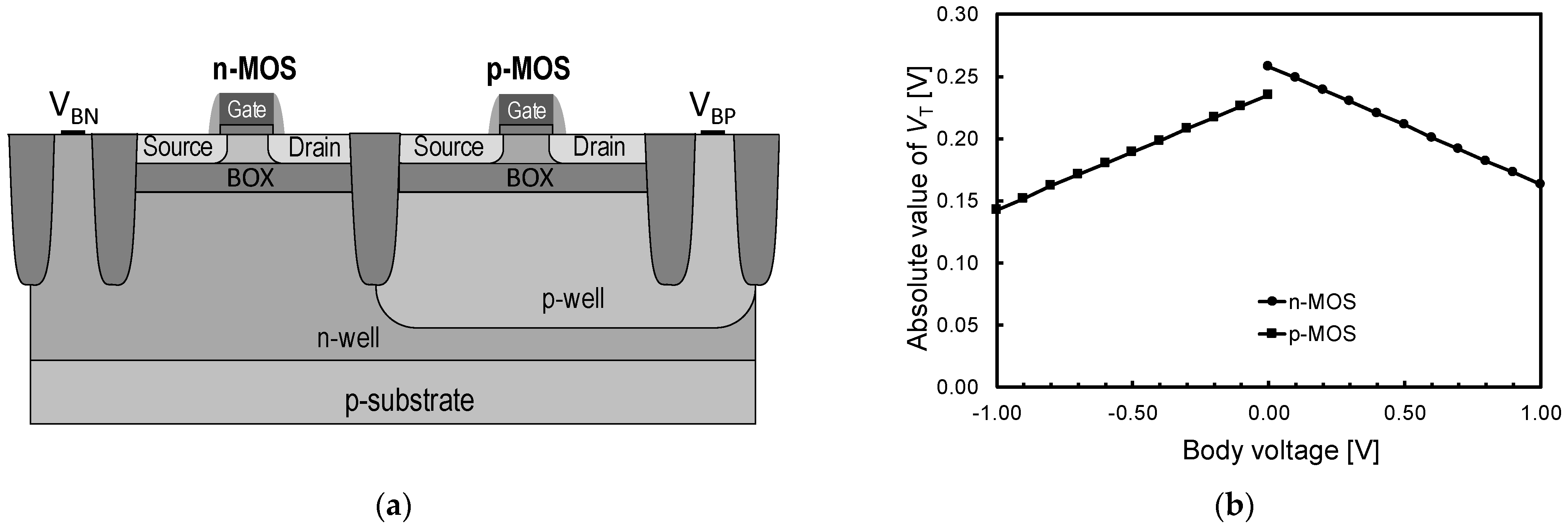
3. The Body Biasing Technique

The body biasing technique can be used to properly modify the threshold voltage, VT, according to the well-known expression reported below for an n-MOS device:
V T = V T 0 + γ ( 2 F V B S 2 F )
where VBS is the voltage between the body and the source, VT0 is the threshold voltage for zero VBS, F is the bulk Fermi potential, and γ is the body effect coefficient. Changing VBS modifies VT, and, thus, the transistor can be operated at a reduced bias voltage, with almost equivalent characteristics in terms of gain, linearity, and noise. Forward (reverse) biasing of n-MOS (p-MOS) transistors has been largely used at low frequencies, but it has also been proven to be effective for RF/mm-wave operations [19,20,21,22,23,24]. It is worth mentioning that for n-MOS (p-MOS) transistors, a forward (reverse) body bias turns on the source-to-body diode, and, thus, an exponential DC current flows across the junction. This produces additional power consumption and can also cause latch-up failure. A simple, but effective, solution to limit the junction current is to add a resistor to the body terminal.
The effectiveness of the body biasing technique is highly increased in the FD-SOI CMOS platform, thanks to a wider VT variation with respect to bulk technologies and the lack of leakage currents. Figure 4a shows the simplified cross-section of a commercial FD-SOI CMOS technology [19,20,21,22,23,24]. Transistors are fabricated in a 7-nm layer of silicon sitting over a 25-nm buried oxide (BOX). An ultra-thin body (UTB) guarantees an isolated electrical conduction channel between the source and drain, since the channel is fully depleted. Figure 4a shows flipped-well low-VT (LVT) transistors that use an n-well body and p-well body for n-MOS and p-MOS devices, respectively. In these transistors, the BOX layer works as a second gate oxide, and the body as a gate terminal (i.e., back gate terminal) that allows the tuning of VT by means of the body voltage. The body gain factor (i.e., the sensitivity of VT to the body voltage) is almost four times that of the traditional bulk technology (i.e., 90 mV/V). The lower VT characteristics of flipped-well devices are well exploited in low-voltage ICs.

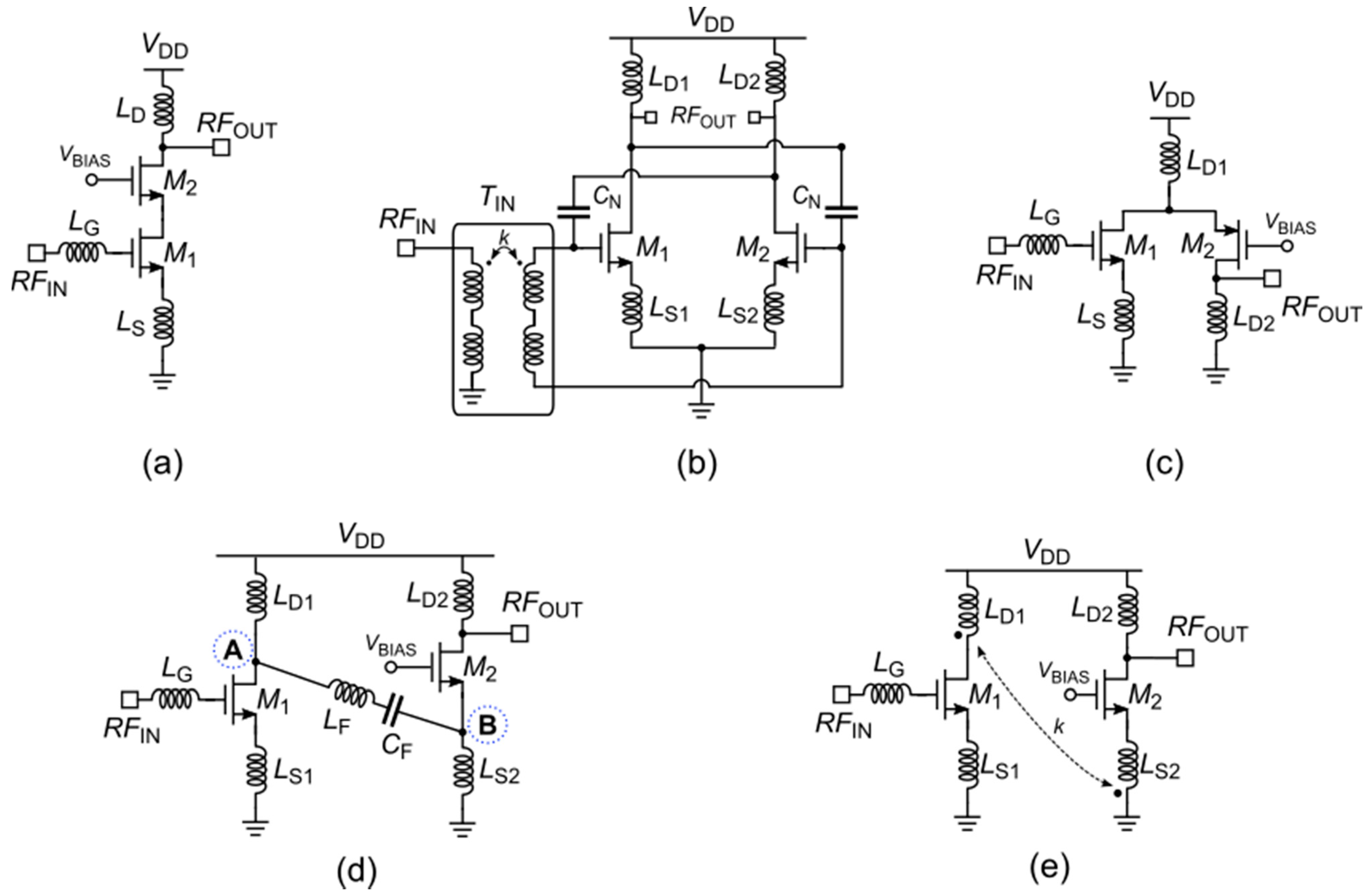
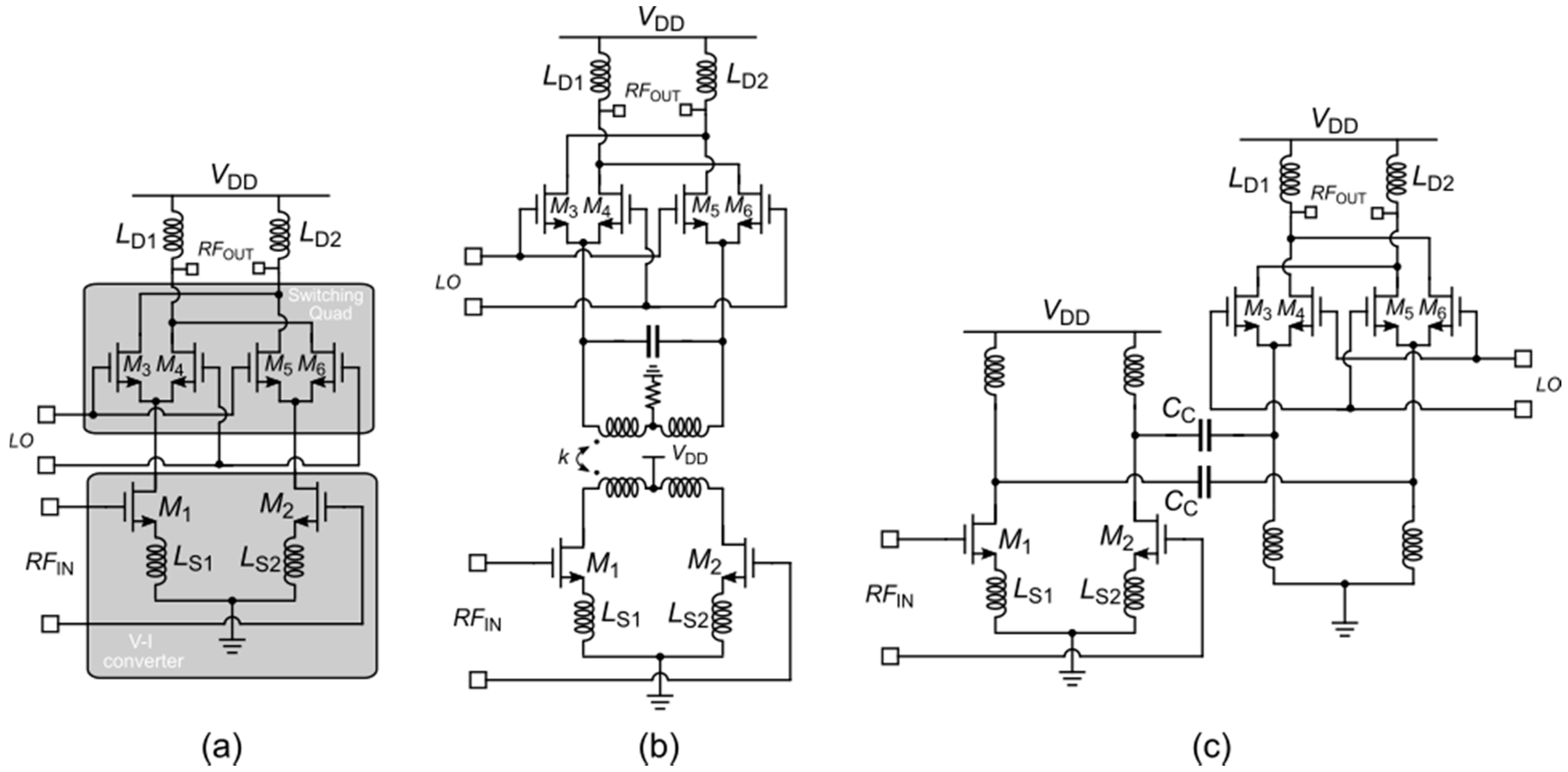
4. Circuit Topologies for Low-Voltage Operation of RF/mm-Wave Blocks

Geometrical scaling enabled RF/mm-wave applications for nanometer CMOS thanks to transition frequency, fT, and maximum oscillation frequency, fMAX, values close to, or even higher than, 200 GHz. Such performance improvements have been obtained at the cost of a considerable reduction in the transistor breakdown voltage (BV), and, consequently, of the maximum supply voltage in comparison with equivalent HBT BiCMOS technologies. This poses new challenges for the design of RF/mm-wave CMOS front ends that are still the very bottleneck for several applications (e.g., 5G, automotive radar, and imaging). The turning point is to properly adjust the well-established RF/mm-wave topologies to mitigate low-voltage operation drawbacks. To this aim, the following simple guidelines can be applied to the main circuit blocks, such as LNA, mixers, and PAs:
Reduce the operative threshold voltage, VT;
Increase the transconductance, gm, by means of positive feedback;
Use only one transistor between the supply voltage, VDD, and ground;
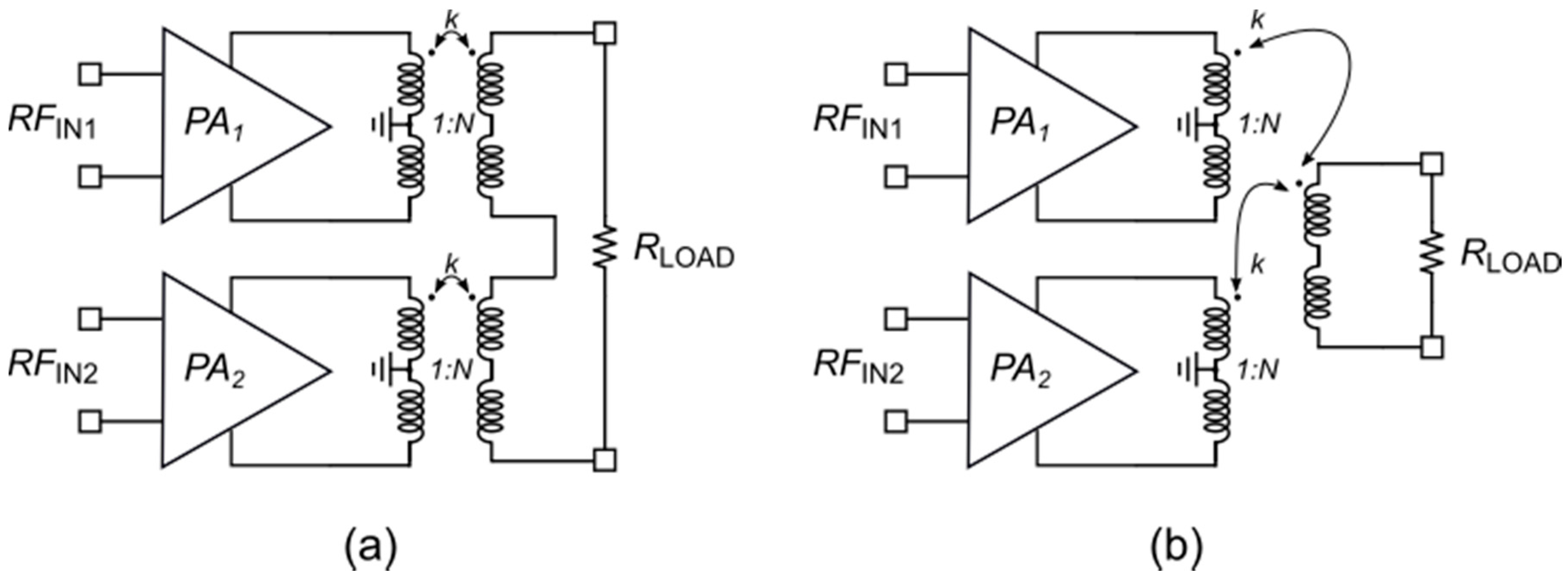
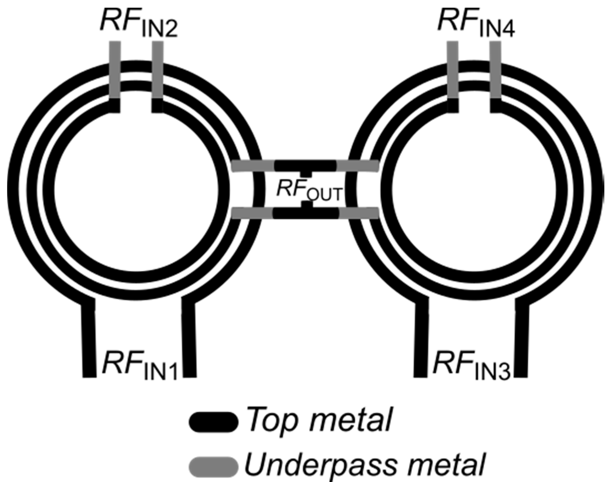
Adopt transformer-based power combining techniques.
A reduction in the VT is strongly suggested to operate the transistor with a lower gate–source voltage, VGS [26]. It can be achieved by exploiting the body biasing technique in standard CMOS, and more profitably in FD-SOI CMOS technologies, as discussed in Section 3. This approach is very effective, but often requires the implementation of additional circuitry, namely, body biasing generators [27,28]. Moreover, reducing VT by means of body biasing could be in contrast with the exploitation of such a technique to compensate for the process–voltage–temperature (PVT) variations, which are typically quite large in nanometer CMOS, especially for automotive applications [29,30].
To further increase the gain performance of a transistor operated at low voltage, positive feedback configurations can be exploited, while trading off degradations of other performance parameters (e.g., noise or linearity) [20]. Several implementations of positive feedback in RF/mm-wave blocks adopt reactive coupling (i.e., inductive or capacitive) or an integrated transformer [31,32,33].
The more effective strategy for the low-voltage operation of RF/mm-wave circuits is to adjust standard topologies to have only one transistor between VDD and the ground. In this perspective, the classical n-MOS cascode topology, largely adopted in high-frequency amplifiers (e.g., LNAs and PAs), thanks to its intrinsic advantages in terms of gain, stability and input–output isolation, cannot be used below a supply voltage of 1 V (i.e., VDD > 2VDS_SAT). Viable circuit alternatives could include the following:
Neutralized common source (CS) topology;
Folded cascode topology;
Reactive resonant coupling: capacitive coupling;
Reactive resonant coupling: transformer coupling.
Figure 5 depicts the low-voltage topologies for an RF/mm-wave LNA stage. It is worth noting that all the reported low-voltage topologies are fully compliant with the standard simultaneous noise/input impedance matching, based on gate, LG, and source, LS, inductance. Moreover, they can also be used to implement a PA stage. The choice of the most suitable solution depends on both the application (e.g., frequency band and current consumption/silicon area specs) and the adopted CMOS technology node.
The CS topology can be adopted for either LNAs [34] or PAs [35,36,37], provided that differential cross-coupled neutralization is used to compensate for the gate–drain capacitances, Cgd, thus improving the input/output isolation and guarantying frequency stability. Neutralization can be implemented with simple integrated capacitors, CN, or by means of an additional pair of MOS transistors, to better track the process variation. Neutralized CS is a very effective solution for low-voltage operations (i.e., VDD > VDS_SAT), but it requires a very careful design to prevent oscillations in the amplifier.
The folded cascode topology takes advantage of the availability of complementary devices with good performance in CMOS technology, but it requires an additional inductor, Ld, with consequent extra silicon area consumption [38]. It is also possible to save silicon area and, at the same time, increase the voltage gain by replacing the inductor with the primary winding of a transformer, whose secondary coil is exploited as a load inductor, LD2. In this way, positive feedback is easily implemented by means of transformer magnetic coupling [31].
Reactive resonant coupling enables the n-MOS cascode topology to also be used at a very low supply voltage, but at the cost of higher current consumption. It can be implemented by using a series resonant LC network (CF, LF), properly sized to exhibit low impedance at the operating frequency, as shown in Figure 5d. Indeed, both inductors, LD1 and LS2, resonate with the capacitances at nodes A and B, respectively. The performance of a capacitive-coupled (CC) cascode amplifier is affected by the Q-factor of the LC network and, especially, of the inductor. Therefore, it can also be used a pure capacitive coupling through by-pass capacitors if the area consumption is tolerable [39].
The transformer-coupled (TC) cascode topology shown in Figure 5e takes advantage of an integrated transformer to couple the common-source and common-gate transistors of a cascode stage [40]. Coupling transformer losses (i.e., winding Q-factors and magnetic coupling factor, k) affect the performance of the TC cascode stage; therefore, resonant mode by means of shunt capacitors (not present in Figure 5e) is mandatory. Moreover, the choice of transformer configuration (i.e., interleaved, stacked or interstacked) is of utmost importance. Generally, the TC cascode topology is area saving in comparison with the CC cascode topology, since it requires a transformer instead of three inductors, excluding the load inductor.
Transformer coupling is also a highly convenient method to implement a low-voltage down- (up)-conversion mixer. Indeed, the traditional configuration of the mixer is based on the double-balanced Gilbert cell topology, shown in Figure 6a, which is not suited to low-voltage operations. It can be easily adjusted by using transformer coupling (TC) between the voltage-to-current (V/I) converter and the Gilbert cell, as shown in Figure 6b [41,42]. This solution also improves the linearity performance (i.e., 1-dB compression point), which is crucial in important applications, such as automotive radars [43]. A capacitive-coupled configuration can also be used as shown in Figure 6c.
CMOS low-voltage operations greatly affect the performance of PAs, especially at the output stage. Indeed, the delivered power is limited by the reduced voltage swing required for device reliability (i.e., drain–source break-down voltage, VDS_MAX). A common solution is to adopt a classical cascode topology made up of a thin-oxide CS transistor and a thick-oxide CG transistor to allow for a higher supply voltage. More complex solutions exploit multistacked devices [44,45]. However, both cascode and multistacked topologies are not viable when the PA is integrated within a transceiver operated at low voltage. In this case, only low-voltage circuit topologies (as shown in Figure 5) can be adopted. However, the achieved output power is not sufficient for the application. Integrated transformers can further increase the output power of an RF/mm-wave PA by exploiting the power-combining technique at the output stage [46,47,48,49,50,51,52,53,54,55,56].
Transformer-based PAs have the following benefits, especially when differential topologies are mandatory:
Implement single-ended-to-differential and differential-to-single-ended conversions, providing inherent virtual ground for differential operations;
Transform impedance for impedance matching and output power matching;
Provide simple DC biasing of power devices via the center tap, avoiding the use of RF chokes and DC blocks.
Moreover, transformers can easily combine the output power of two devices, thus nearly doubling the overall power (if the losses of the combining network are negligible). Power combining can be obtained by using voltage-combining transformers (VCTs) or current-combining transformers (CCTS), which are also known as series or parallel combining, respectively.
Figure 7 depicts a two-way implementation for voltage- and current-combining techniques, by using integrated transformers with a 1:N turn ratio. The voltage-combining technique is aimed at summing the voltage produced by each PA unit by exploiting stacked secondary windings, in order to increase the output voltage and, thus, the delivered power of low-voltage CMOS PAs. On the other hand, the current-combining technique is aimed at gathering the current of each PA unit by exploiting the parallel-coupled secondary winding to increase the overall current, thus boosting the output power.
By extending these techniques to M PA units, the output power can be theoretically boosted up to M time, either by using series or parallel combining.
Physical implementations of power combining are greatly influenced by the specific application and adopted integration technology. An important limitation is caused by the integrated transformers, whose losses have to be properly minimized to preserve the power-combining advantage with reasonable silicon area consumption. Figure 8 depicts the simplified layout of an example of a series-combining transformer for the voltage-combining topology in Figure 7a. The transformer exploits only two metal layers (i.e., the upper and thicker metal layers) for both windings, which are coupled by means of an interleaved configuration.
Unfortunately, both series- and parallel-combining techniques have practical design limitations on the maximum number of PA units that can be profitably combined. Specifically, in the voltage-combining technique, the number of PA units is limited by the optimal impedance of each power device, ROPT, and is equal to the following:
R OPT = R LOAD 2 · M S · N 2
where RLOAD, MS, and N are the load resistance, the number of PA units and the transformer turn ratio, respectively. Indeed, according to Equation (2), when MS increases, ROPT reduces, thus requiring larger power transistors with lower maximum available gain, due to the RLC parasitics. Therefore, voltage combining is not used for an MS higher than four.
On the other hand, in the current-combining technique, ROPT is equal to the following:
R OPT = M P 2 · N 2 R LOAD
where RLOAD, MP, and N are the load resistance, the number of PA units and the transformer turn ratio, respectively. From Equation (3), it is evident that the current-combining technique is more flexible in the selection of the optimum resistance, since the turn ratio, N, can be properly used to tune the optimum impedance, ROPT. In particular, a larger turn ratio is required to lower the ROPT when a higher MP is used. Unfortunately, increasing N often produces lossy and area-consuming integrated transformers. Moreover, only integer number turn ratios can be practically implemented.
These drawbacks can be overcome by using a hybrid-combining technique, based on both series and parallel transformers. Figure 9 shows two types of hybrid-combining topologies, namely, voltage–current combining (SPCT) and current–voltage combining (PSCT), both implemented for MS = MP = 2. Generally, the output powers of MS × MP PA units can be increased up to MS × MP times. This hybrid approach gives more freedom to designers, with respect to pure voltage or current technique, since the optimum resistance is given by the following:
R OPT = M P ·   M S 2 · N 2 R LOAD
Figure 10 depicts an example of a series–parallel-combining transformer for the circuit topology in Figure 9a. The transformer combines four PA units by means of interleaved coupling, thus requiring only two metal layers. Moreover, the structure maximizes the use of the top metal layer (i.e., the thicker layer of a standard CMOS BEOL), while reducing the need for the second metal layer, which is exclusively used for the underpass connections. It is worth noting that stacked coupling could be used to increase the magnetic coupling and save silicon area, but stacked transformers require at least two thick metal layers to have an advantage [18].

5. Conclusions

This paper has provided the reader with an overview of state-of-the-art low-voltage design techniques for RF/mm-wave ICs, from body biasing for low-VT operations of nanometer CMOS transistors to reactive resonant coupling for sub 1-V circuits. A special insight was dedicated to transformer-based power-combining approaches to boost the PA output power, especially at mm-wave frequencies. Thanks to proper combinations of the described techniques, several high-frequency applications can be addressed by using sub 1-V CMOS ICs. This process started with RF wireless communications and now involves mm-wave applications, such as W-band automotive radar and beyond. Nanometer FD-SOI CMOS technologies are the natural candidates for future low-voltage RF/mm-wave ICs, especially with thick BEOL for better passive components.

Funding

This work was supported in part by the University of Catania through the Project “Programma Ricerca di Ateneo UNICT 2020-22 linea 2”.

Institutional Review Board Statement

Not applicable.

Informed Consent Statement

Not applicable.

Data Availability Statement

The data presented in this study are available on request from the corresponding author.

Conflicts of Interest

The author declares no conflict of interest.

References

  1. Joseph, A.; Jain, V.; Ong, S.N.; Wolf, R.; Lim, S.F.; Singh, J. Technology Positioning for Mm Wave Applications: 130/90nm SiGe BiCMOS vs. 28nm RFCMOS. In Proceedings of the 2018 IEEE BiCMOS and Compound Semiconductor Integrated Circuits and Technology Symposium (BCICTS), San Diego, CA, USA, 15–17 October 2018; pp. 18–21. [Google Scholar]
  2. Cathelin, A. Fully Depleted Silicon on Insulator Devices CMOS: The 28-Nm Node Is the Perfect Technology for Analog, RF, MmW, and Mixed-Signal System-on-Chip Integration. IEEE Solid-State Circuits Mag. 2017, 9, 18–26. [Google Scholar] [CrossRef]
  3. Girlando, G.; Ragonese, E.; Palmisano, G. Silicon Bipolar LNAs in the X and Ku Bands. Analog. Integr. Circuits Signal Process. 2004, 41, 119–127. [Google Scholar] [CrossRef]
  4. Ragonese, E.; Scuderi, A.; Giammello, V.; Palmisano, G. A SiGe BiCMOS 24-GHz Receiver Front-End for Automotive Short-Range Radar. Analog. Integr. Circuits Signal Process. 2011, 67, 121–130. [Google Scholar] [CrossRef]
  5. Sapone, G.; Ragonese, E.; Italia, A.; Palmisano, G. A 0.13-µm SiGe BiCMOS Colpitts-Based VCO for W-Band Radar Transmitters. IEEE Trans. Microw. Theory Tech. 2013, 61, 185–194. [Google Scholar] [CrossRef]
  6. Giammello, V.; Ragonese, E.; Palmisano, G. A Transformer-Coupling Current-Reuse SiGe HBT Power Amplifier for 77-GHz Automotive Radar. IEEE Trans. Microw. Theory Tech. 2012, 60, 1676–1683. [Google Scholar] [CrossRef]
  7. Giammello, V.; Ragonese, E.; Palmisano, G. A 24/77-GHz SiGe BiCMOS Transmitter Chipset for Automotive Radar. Microw. Opt. Technol. Lett. 2013, 55, 782–786. [Google Scholar] [CrossRef]
  8. Scuderi, A.; Ragonese, E.; Biondi, T.; Palmisano, G. Integrated Inductors and Transformers: Characterization, Design and Modeling for RF and mm-Wave Applications; CRC Press: Boca Raton, FL, USA, 2010. [Google Scholar]
  9. Spataro, S.; Ragonese, E. Design and Optimization of Silicon-Integrated Inductive Components for Automotive Radar Applications in K- and W-Bands. In Proceedings of the 2020 AEIT International Conference of Electrical and Electronic Technologies for Automotive (AEIT AUTOMOTIVE), Turin, Italy, 18–20 November 2020; pp. 1–6. [Google Scholar]
  10. Craninckx, J.; Steyaert, M.S.J. A 1.8-GHz Low-Phase-Noise CMOS VCO Using Optimized Hollow Spiral Inductors. IEEE J. Solid-State Circuits 1997, 32, 736–744. [Google Scholar] [CrossRef] [Green Version]
  11. Yim, S.M.; Chen, T. The Effects of a Ground Shield on the Characteristics and Performance of Spiral Inductors. IEEE J. Solid-State Circuits 2002, 37, 237–244. [Google Scholar] [CrossRef]
  12. Spataro, S.; Salerno, N.; Papotto, G.; Ragonese, E. The Effect of a Metal PGS on the Q-Factor of Spiral Inductors for RF and mm-Wave Applications in a 28-nm CMOS Technology. Int. J. RF Microw. Comput.-Aided Eng. 2020, 30, e22368. [Google Scholar] [CrossRef]
  13. Bevilacqua, A. Fundamentals of Integrated Transformers: From Principles to Applications. IEEE Solid-State Circuits Mag. 2020, 12, 86–100. [Google Scholar] [CrossRef]
  14. Ragonese, E.; Sapone, G.; Palmisano, G. High-Performance Interstacked Transformers for mm-Wave ICs. Microw. Opt. Technol. Lett. 2010, 52, 2160–2163. [Google Scholar] [CrossRef]
  15. Ragonese, E.; Sapone, G.; Giammello, V.; Palmisano, G. Analysis and Modeling of Interstacked Transformers for Mm-Wave Applications. Analog. Integr. Circuits Signal Process. 2012, 72, 121–128. [Google Scholar] [CrossRef]
  16. Giammello, V.; Ragonese, E.; Palmisano, G. A 77-GHz PA with Ground-Plane Parasitic Cancellation in a SiGe HBT BiCMOS Technology. Microw. Opt. Technol. Lett. 2011, 53, 1413–1416. [Google Scholar] [CrossRef]
  17. Avenier, G.; Diop, M.; Chevalier, P.; Troillard, G.; Loubet, N.; Bouvier, J.; Depoyan, L.; Derrier, N.; Buczko, M.; Leyris, C.; et al. 0.13 m SiGe BiCMOS Technology Fully Dedicated to mm-Wave Applications. IEEE J. Solid State Circuits 2009, 44, 2312–2321. [Google Scholar] [CrossRef]
  18. Ragonese, E.; Nocera, C.; Cavarra, A.; Papotto, G.; Spataro, S.; Palmisano, G. A Comparative Analysis between Standard and mm-Wave Optimized BEOL in a Nanoscale CMOS Technology. Electronics 2020, 9, 2124. [Google Scholar] [CrossRef]
  19. Lin, W.; Tsai, J.; Jen, Y.; Huang, T.; Wang, H. A 0.7-V 60-GHz Low-Power LNA with Forward Body Bias Technique in 90 nm CMOS Process. In Proceedings of the 2009 European Microwave Conference (EuMC), Rome, Italy, 29 September–1 October 2009; pp. 393–396. [Google Scholar]
  20. Dehqan, A.; Kargaran, E.; Mafinezhad, K.; Nabovati, H. Design of 0.45V, 1.3mW Ultra High Gain CMOS LNA Using Gm-Boosting and Forward Body Biasing Technique. In Proceedings of the 2012 IEEE 55th International Midwest Symposium on Circuits and Systems (MWSCAS), Boise, ID, USA, 5–8 August 2012; pp. 722–725. [Google Scholar]
  21. Chou, H.; Ke, Z.; Chiou, H. A Low Power Compact Size Forward Body-Biased K-Band CMOS Low Noise Amplifier. In Proceedings of the Asia-Pacific Microwave Conference 2011, Melbourne, VIC, Australia, 5–8 December 2011; pp. 494–497. [Google Scholar]
  22. Parvizi, M.; Allidina, K.; El-Gamal, M.N. Short Channel Output Conductance Enhancement through Forward Body Biasing to Realize a 0.5 V 250 μW 0.6–4.2 GHz Current-Reuse CMOS LNA. IEEE J. Solid-State Circuits 2016, 51, 574–586. [Google Scholar] [CrossRef]
  23. Tochou, G.; Cathelin, A.; Frappé, A.; Kaiser, A.; Rabaey, J. Impact of Forward Body-Biasing on Ultra-Low Voltage Switched-Capacitor RF Power Amplifier in 28 nm FD-SOI. IEEE Trans. Circuits Syst. II Express Briefs 2022, 69, 50–54. [Google Scholar] [CrossRef]
  24. Kane, O.M.; Lucci, L.; Scheiblin, P.; Poiroux, T.; Barbé, J.-C.; Danneville, F. Back Gate Impact on the Noise Performances of 22FDX Fully-Depleted SOI CMOS. In Proceedings of the 2020 15th European Microwave Integrated Circuits Conference (EuMIC), Utrecht, The Netherlands, 10–15 January 2021; pp. 81–84. [Google Scholar]
  25. Finocchiaro, A.; Papotto, G.; Ragonese, E.; Palmisano, G. A 28-nm FD-SOI CMOS Variable-Gain Amplifier with Body-Bias-Based DC-Offset Cancellation for Automotive Radars. IEEE Trans. Circuits Syst. II Express Briefs 2019, 66, 1693–1697. [Google Scholar] [CrossRef]
  26. El-Aassar, O.; Rebeiz, G.M. Design of Low-Power Sub-2.4 dB Mean NF 5G LNAs Using Forward Body Bias in 22 nm FDSOI. IEEE Trans. Microw. Theory Tech. 2020, 68, 4445–4454. [Google Scholar] [CrossRef]
  27. Justo, D.; Cavalheiro, D.; Moll, F. Body Bias Generators for Ultra Low Voltage Circuits in FDSOI Technology. In Proceedings of the 2017 32nd Conference on Design of Circuits and Integrated Systems (DCIS), Barcelona, Spain, 22–24 November 2017; pp. 1–6. [Google Scholar]
  28. Wang, L.; Wu, C.; Feng, L.; Chang, A.; Lian, Y. A Low-Power Forward and Reverse Body Bias Generator in CMOS 40 nm. IEEE Trans. Very Large Scale Integr. (VLSI) Syst. 2018, 26, 1403–1407. [Google Scholar] [CrossRef]
  29. Gomez, R.; Dutto, C.; Huard, V.; Clerc, S.; Bano, E.; Flatresse, P. Design Methodology with Body Bias: From Circuit to Engineering. In Proceedings of the 2017 IEEE SOI-3D-Subthreshold Microelectronics Technology Unified Conference (S3S), Burlingame, CA, USA, 16–19 October 2017; pp. 1–4. [Google Scholar]
  30. de Streel, G.; Stas, F.; Gurné, T.; Durant, F.; Frenkel, C.; Cathelin, A.; Bol, D. SleepTalker: A ULV 802.15.4a IR-UWB Transmitter SoC in 28-nm FDSOI Achieving 14 PJ/b at 27 Mb/s With Channel Selection Based on Adaptive FBB and Digitally Programmable Pulse Shaping. IEEE J. Solid-State Circuits 2017, 52, 1163–1177. [Google Scholar] [CrossRef]
  31. Kihara, T.; Park, H.-J.; Takobe, I.; Yamashita, F.; Matsuoka, T.; Taniguchi, K. A 0.5 V Area-Efficient Transformer Folded-Cascode Low-Noise Amplifier in 90 nm CMOS. In Proceedings of the 2008 IEEE International Conference on Integrated Circuit Design and Technology and Tutorial, Grenoble, France, 2–4 June 2008; pp. 21–24. [Google Scholar]
  32. Kundu, S.; Khairi, A.; Paramesh, J. A Supply-Voltage Scalable, 45 nm CMOS Ultra-Wideband Receiver for mm-Wave Ranging and Communication. In Proceedings of the IEEE 2012 Custom Integrated Circuits Conference, San Jose, CA, USA, 9–12 September 2012; pp. 1–4. [Google Scholar]
  33. Lin, Y.-H.; Hsiao, S.-C.; Tsai, J.-H.; Huang, T.-W. A 0.7-mW V-Band Transformer-Based Positive- Feedback Receiver Front-End in a 65-nm CMOS. IEEE Microw. Wirel. Compon. Lett. 2020, 30, 613–616. [Google Scholar] [CrossRef]
  34. Liang, C.-J.; Chiang, C.-W.; Zhou, J.; Huang, R.; Wen, K.-A.; Chang, M.-C.F.; Kuan, Y.-C. A 0.6-V VDD W-Band Neutralized Differential Low Noise Amplifier in 28-nm Bulk CMOS. IEEE Microw. Wirel. Compon. Lett. 2021, 31, 481–484. [Google Scholar] [CrossRef]
  35. Asada, H.; Matsushita, K.; Bunsen, K.; Okada, K.; Matsuzawa, A. A 60GHz CMOS Power Amplifier Using Capacitive Cross-Coupling Neutralization with 16% PAE. In Proceedings of the 2011 41st European Microwave Conference, Manchester, UK, 10–11 October 2011; pp. 1115–1118. [Google Scholar]
  36. Chen, L.; Zhang, L.; Wang, Y.; Yu, Z. A Compact E-Band Power Amplifier with Gain-Boosting and Efficiency Enhancement. IEEE Trans. Microw. Theory Tech. 2020, 68, 4620–4630. [Google Scholar] [CrossRef]
  37. Nocera, C.; Papotto, G.; Cavarra, A.; Ragonese, E.; Palmisano, G. A 13.5-dBm 1-V Power Amplifier for W-Band Automotive Radar Applications in 28-Nm FD-SOI CMOS Technology. IEEE Trans. Microw. Theory Tech. 2021, 69, 1654–1660. [Google Scholar] [CrossRef]
  38. Kargaran, E.; Nabovati, G.; Mafinezhad, K.; Nabovati, H. An Ultra Low Voltage Ultra Low Power Folded Cascode CMOS LNA Using Forward Body Bias Technology for GPS Application. In Proceedings of the 2011 19th Iranian Conference on Electrical Engineering, Tehran, Iran, 17–19 May 2011; pp. 1–11. [Google Scholar]
  39. Manku, T.; Beck, G.; Shin, E.J. A Low-Voltage Design Technique for RF Integrated Circuits. IEEE Trans. Circuits Syst. II Analog. Digit. Signal Process. 1998, 45, 1408–1413. [Google Scholar] [CrossRef]
  40. Giammello, V.; Ragonese, E.; Palmisano, G. Transformer-Coupled Cascode Stage for mm-Wave Power Amplifiers in Sub-mm CMOS Technology. Analog. Integr. Circuits Signal Process. 2011, 66, 449–453. [Google Scholar] [CrossRef]
  41. Hanay, O.; Negra, R. 0.33 mm2 13.3 dB Gain Sub-6 GHz to 28 GHz Transformer-Coupled Low-Voltage Upconversion Mixer for 5G Applications. In Proceedings of the ESSCIRC 2021—IEEE 47th European Solid State Circuits Conference (ESSCIRC), Grenoble, France, 13–22 September 2021; pp. 373–376. [Google Scholar]
  42. Nocera, C.; Cavarra, A.; Ragonese, E.; Palmisano, G.; Papotto, G. Down-Converter Solutions for 77-GHz Automotive Radar Sensors in 28-Nm FD-SOI CMOS Technology. In Proceedings of the 2018 14th Conference on Ph.D. Research in Microelectronics and Electronics (PRIME), Prague, Czech Republic, 2–5 July 2018; pp. 153–156. [Google Scholar]
  43. Papotto, G.; Nocera, C.; Finocchiaro, A.; Parisi, A.; Cavarra, A.; Castorina, A.; Ragonese, E.; Palmisano, G. A 27-mW W-Band Radar Receiver with Effective TX Leakage Suppression in 28-nm FD-SOI CMOS. IEEE Trans. Microw. Theory Tech. 2021, 69, 4132–4141. [Google Scholar] [CrossRef]
  44. Kim, Y.; Kwon, Y. Analysis and Design of Millimeter-Wave Power Amplifier Using Stacked-FET Structure. IEEE Trans. Microw. Theory Tech. 2015, 63, 691–702. [Google Scholar] [CrossRef]
  45. Manente, D.; Padovan, F.; Seebacher, D.; Bassi, M.; Bevilacqua, A. A 28-GHz Stacked Power Amplifier with 20.7-dBm Output P1dB in 28-nm Bulk CMOS. IEEE Solid-State Circuits Lett. 2020, 3, 170–173. [Google Scholar] [CrossRef]
  46. Niknejad, A.M.; Chowdhury, D. Transforming RF and mm-Wave CMOS Circuits. In Proceedings of the 2009 International Symposium on VLSI Design, Automation and Test, Hsinchu, Taiwan, 28–30 April 2009; pp. 138–141. [Google Scholar]
  47. Zhou, P.; Chen, J.; Hong, W.; Gao, H. A 77-GHz Fully Integrated Power Amplifier for Automotive Radar Application in 40-nm CMOS. In Proceedings of the 2021 IEEE MTT-S International Wireless Symposium (IWS), Nanjing, China, 23–26 May 2021; pp. 1–3. [Google Scholar]
  48. An, K.H.; Lee, O.; Kim, H.; Lee, N.H.; Han, J.; Yang, K.S.; Kim, Y.; Chang, J.J.; Woo, W.; Lee, C.-H.; et al. Power-Combining Transformer Techniques for Fully-Integrated CMOS Power Amplifiers. IEEE J. Solid State Circuits 2008, 43, 1064–1075. [Google Scholar] [CrossRef]
  49. Sandstrom, D.; Martineau, B.; Varonen, M.; Karkkainen, M.; Cathelin, A.; Halonen, K.A.I. 94 GHz power-combining power amplifier with +13 dBm saturated output power in 65 nm CMOS. In Proceedings of the IEEE Radio Frequency Integrated Circuits Symp, Baltimore, MD, USA, 5–7 June 2011; pp. 1–4. [Google Scholar]
  50. Gu, Q.J.; Xu, Z.; Chang, M.F. Two-Way Current-Combining W-Band Power Amplifier in 65-Nm CMOS. IEEE Trans. Microw. Theory Tech. 2012, 60, 1365–1374. [Google Scholar] [CrossRef]
  51. Comeau, J.P.; Thoenes, E.W.; Imhoff, A.; Morton, M.A. X-Band +24 dBm CMOS Power Amplifier with Transformer Power Combining. In Proceedings of the 2011 IEEE 11th Topical Meeting on Silicon Monolithic Integrated Circuits in RF Systems, Glendale, AZ, USA, 17–19 January 2011; pp. 49–52. [Google Scholar]
  52. Chen, J.; Niknejad, A.M. A Compact 1V 18.6dBm 60GHz Power Amplifier in 65nm CMOS. In Proceedings of the 2011 IEEE International Solid-State Circuits Conference, San Francisco, CA, USA, 20–24 February 2011; pp. 432–433. [Google Scholar]
  53. Trinh, V.-S.; Park, J.-D. A 25.1 dBm 25.9-dB Gain 25.4% PAE X-Band Power Amplifier Utilizing Voltage Combining Transformer in 65-nm CMOS. IEEE Access 2021, 9, 6513–6521. [Google Scholar] [CrossRef]
  54. Li, S.; Rebeiz, G.M. A 130–151 GHz 8-Way Power Amplifier with 16.8–17.5 dBm Psat and 11.7–13.4% PAE Using CMOS 45 nm RFSOI. In Proceedings of the 2021 IEEE Radio Frequency Integrated Circuits Symposium (RFIC), Atlanta, GA, USA, 7–9 June 2021; pp. 115–118. [Google Scholar]
  55. Trinh, V.-S.; Park, J.-D. An 85-GHz Power Amplifier Utilizing a Transformer-Based Power Combiner Operating Beyond the Self-Resonance Frequency. IEEE J. Solid-State Circuits 2021, 1. [Google Scholar] [CrossRef]
  56. Yang, B.; Qian, H.J.; Wang, T.; Luo, X. 1.2–3.6 GHz 32.67 dBm 4096-QAM Digital PA Using Reconfigurable Power Combining Transformer for Wireless Communication. In Proceedings of the 2020 IEEE Radio Frequency Integrated Circuits Symposium (RFIC), Los Angeles, CA, USA, 4–6 August 2020; pp. 123–126. [Google Scholar]
Figure 1. (a) SEM cross-section of a silicon-integrated spiral inductor; (b) simplified representation of main loss phenomena in silicon-integrated inductive components. Reprinted with permission from Ref [9]. Copyright 2020, IEEE.
Applsci 12 02103 g001
Figure 2. Integrated transformer configurations for RF/mm-wave operation. Reprinted with permission from Ref [9]. Copyright 2020, IEEE.
Applsci 12 02103 g002
Figure 3. BEOL comparison between (a) mm-wave-optimized BiCMOS technology [17] and (b) 28-nm CMOS technology with standard BEOL [2], Reprinted from Ref [18].
Applsci 12 02103 g003
Figure 4. The 28-nm FD-SOI CMOS technology: (a) simplified cross-section of LVT flipped-well transistors, (b) VT variation with respect to the body voltage for the LVT flipped-well devices. Reprinted with permission from Ref [25]. Copyright 2019, IEEE.
Applsci 12 02103 g004
Figure 5. (a) Cascode; (b) neutralized common source (CS); (c) folded cascode; (d) capacitive-coupled (CC) cascode; (e) transformer-coupled (TC) cascode.
Applsci 12 02103 g005
Figure 6. Double-balanced mixer topologies: (a) traditional Gilbert cell mixer; (b) TC Gilbert cell mixer; (c) CC Gilbert cell mixer.
Applsci 12 02103 g006
Figure 7. Power-combining techniques (a): voltage-combining (SCT), (b) current-combining (PCT).
Applsci 12 02103 g007
Figure 8. Example of an SCT for PA voltage combining.
Applsci 12 02103 g008
Figure 9. Power-combining techniques (a): voltage–current combining (SPCT); (b) current–voltage combining (PSCT).
Applsci 12 02103 g009
Figure 10. Example of a series–parallel-combining transformer (SPCT) for 4 PA voltage–current combining.
Applsci 12 02103 g010
Table 1. Layout/process parameters vs. electrical performance of an integrated inductor.
Inductor
Parameters
Peak Q-Factor
(QMAX)
Low-Frequency Inductance
(LDC)
Self-Resonance Frequency
(SRF)
Number of turns, n
Metal width, w
Metal spacing, s
Fill ratio, ρ▲▼▲▼
Metal thickness, t
Oxide thickness tox
Substrate resistivity, ρSI
▲ increase; ▼ decrease; ▲▼ optimum; — constant.
Table 2. Pros and cons of different integrated transformer configurations.
Performance ParametersTransformer Structures
InterleavedStackedInterstackedStacked Folded
Magnetic coupling factor, k++++++++
Winding Q-factors+++++++
Self-resonance frequency (SRF)+++++++
Turn ratio, N++ +--
Publisher’s Note: MDPI stays neutral with regard to jurisdictional claims in published maps and institutional affiliations.

