1. Introduction
The power generated by the renewable energy system is processed through power converters for grid system integration. The voltage and frequency of the electrical power at the distribution level are maintained constant. But in some applications, the regulation of voltage and frequency is required according to the demand. These areas include grid or load voltage control, heating processes that depend upon the high-frequency induction phenomena, and motor speed control systems. In an electric traction system, the speed control of the induction motor is governed through the frequency regulation in step-down mode at a constant voltage. Similarly, for the induction heating process of the heating load, the grid standard or fixed frequency is to be controlled in a boost fashion. Normally these targets are achieved through AC-AC converters that regulate the characteristics of the output through voltage and frequency control. In these converters, two power conversion approaches are adopted depending on the requirements. In the first scenario, input AC power is converted to DC and then it is converted back to AC power with adjusted voltage and frequency. This power conversion approach is indirect and power converters realized through this scheme are called indirect AC-AC converters. The second approach is called direct AC-AC converters where the power conversion process is realized in a single conversion stage.
In conventional indirect power converting approaches as in [
1], the first stage is rectification that transforms the grid AC power to DC that is stored in a DC link capacitor. Then this DC power is transformed to AC power with required output characteristics. The main concern in this realization is a large count of switching and passive components. The number of switching devices is decreased in the indirect converters realized with three inverter legs as pinpointed in [
2]. Here, both the rectification and inversion stage share the middle leg of the converter. This approach has low conversion losses as that of the four-leg converters with the same dc-link voltage and power quality. The power quality of the output voltage is improved in the three-leg converter by increasing the output voltage levels [
3,
4,
5,
6]. These converting topologies are attractive as they have low switching voltage and improved power quality. But all these characteristics are ensured on the cost of circuit and control complication.
The issues related to a dc-link capacitor are tackled in direct AC-AC converters. These power converting topologies lower the maintenance requirements and overall system losses. Their use becomes more valuable for load or grid voltage control as they are realized with a lower number of switching units. The use of external power storage devices is also eliminated in their realization [
7,
8]. The direct AC-AC circuit may be realized with basic DC-DC topologies that include the buck, boost, or buck-boost. The merits of these topologies include simple circuit and control schemes but there are commutation issues due to the use of bidirectional or AC switches [
9]. This problem may be tackled either by connecting the RC protection circuit across the switching units or by employing soft commutation techniques. The power losses in the RC circuit degrade the power quality of the output as they distort the outputs. The use of RC protection circuits is eliminated in some novel AC-AC power converting topologies as reported in [
10,
11]. But these topologies lack bipolar voltage characteristics so they can only be employed to resolve either voltage sag or swell issues. They cannot be employed as frequency controllers. Z-source structure is employed in [
12,
13] to ensure both polarities of the output voltage but their realization has certain drawbacks including abrupt change in voltage. Also, their size and response time increases as high-order passive components are present in the z-source circuit arrangement. These drawbacks are tackled in the converters as reported in [
14,
15]. They are realized without involving the RC or z-source circuit for safe commutation but their non-inverting and inverting operations are non-identical. The converters represented in [
16,
17] tackle the non-identical operations of the preceding converters. The converters having positive and negative voltage gain may also be employed as frequency controllers as discussed in [
18]. Their power quality during inverting operation is poor as that of non-inverting operation as their operating modes are non-symmetrical. The symmetrical operating modes are obtained in [
19] but this topology has the problem of high conversion losses as it can only be realized in buck-boost fashion. The conversion efficiency is improved in [
20] by enabling the buck and boost operation with a voltage gain of dual polarities. The converters presented in [
18,
19,
20] can be effectively operated in low-frequency operation but switching techniques in their high-frequency operation become complicated that reduces their potency in frequency boost operation.
A simple switching algorithm is proposed in [
21] for induction heating systems but it faces the challenge of a large number of switching units. The number of switching units is reduced in [
22] with a similar switching scheme. The harmonic issues in direct ac voltage and frequency converters are reported in [
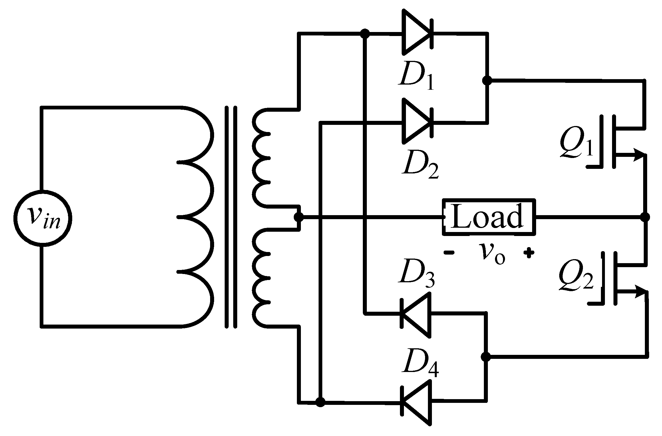
23] to evaluate their performance with other power converting topologies. A compact power converting topology as depicted in
Figure 1 is reported in [
24] to lower the conduction losses by reducing the number of switching units.
This topology is unable to realize without a bulky center-tapped transformer that is operated at low grid frequency. Its use not only increases the overall size and cost but also leads toward the core saturation issue owing to the flow of unidirectional currents or low-frequency currents in outputs windings. Also, there is a shoot-through issue especially one output frequency requirement is much higher than that of input standard frequency due to the complementary switching structure of the controlled switching units “Q1” and “Q2.”
In viewing the above issues reported in the preceding research articles, a new transformer -less direct AC-AC power converting topology is suggested and has the following attractive characteristics.
It has no core saturation issue and no core losses, as the proposed topology is directly connected to the grid supply. This elimination decreases the overall volume and improves conversion efficiency.
An intermediate inductor ensures the shoot-through challenge once complementary operated switching units are turned on at the same time. The shoot-through or overlapping intervals may be employed to increase the boost factor during the frequency step-up operation.
Any low-cost PWM controller may be employed due to the use of simple switching techniques.
All operating modes are realized at zero voltage switching in frequency regulation modes.
For the sake of organizing this research article,
Section 2 investigates the operating modes for voltage and frequency control with the help of switching signals. A comparison of the performance characteristics of the proposed topology with the existing converters is addressed in
Section 3.
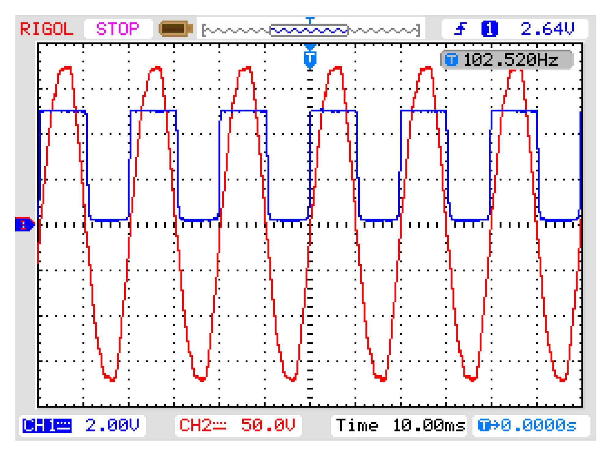
Section 4 illustrates the effectiveness of the developed topology by using simulation and practical results.
Section 5 highlights the conclusion.
2. Suggested Topology and Its Operation
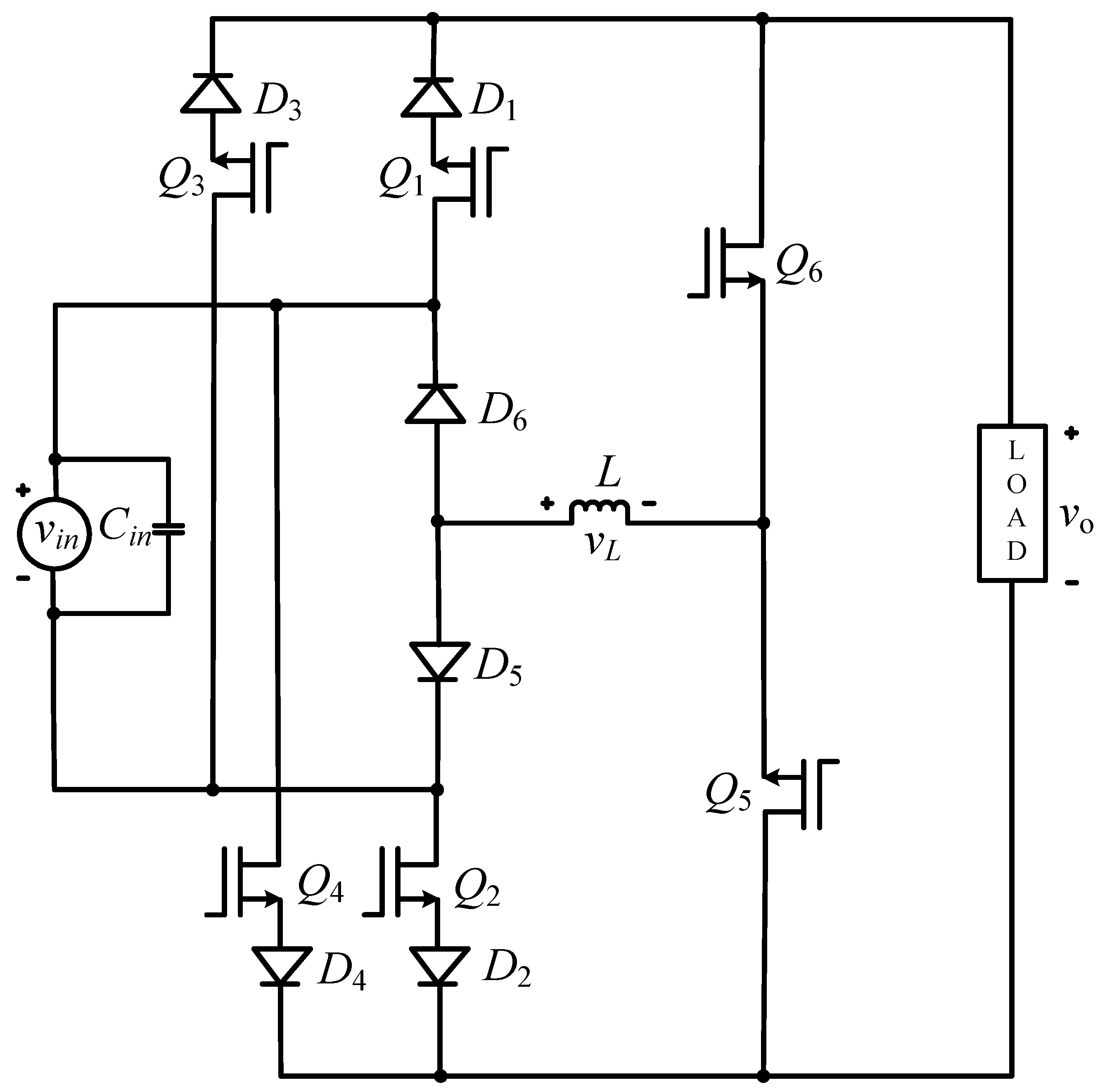
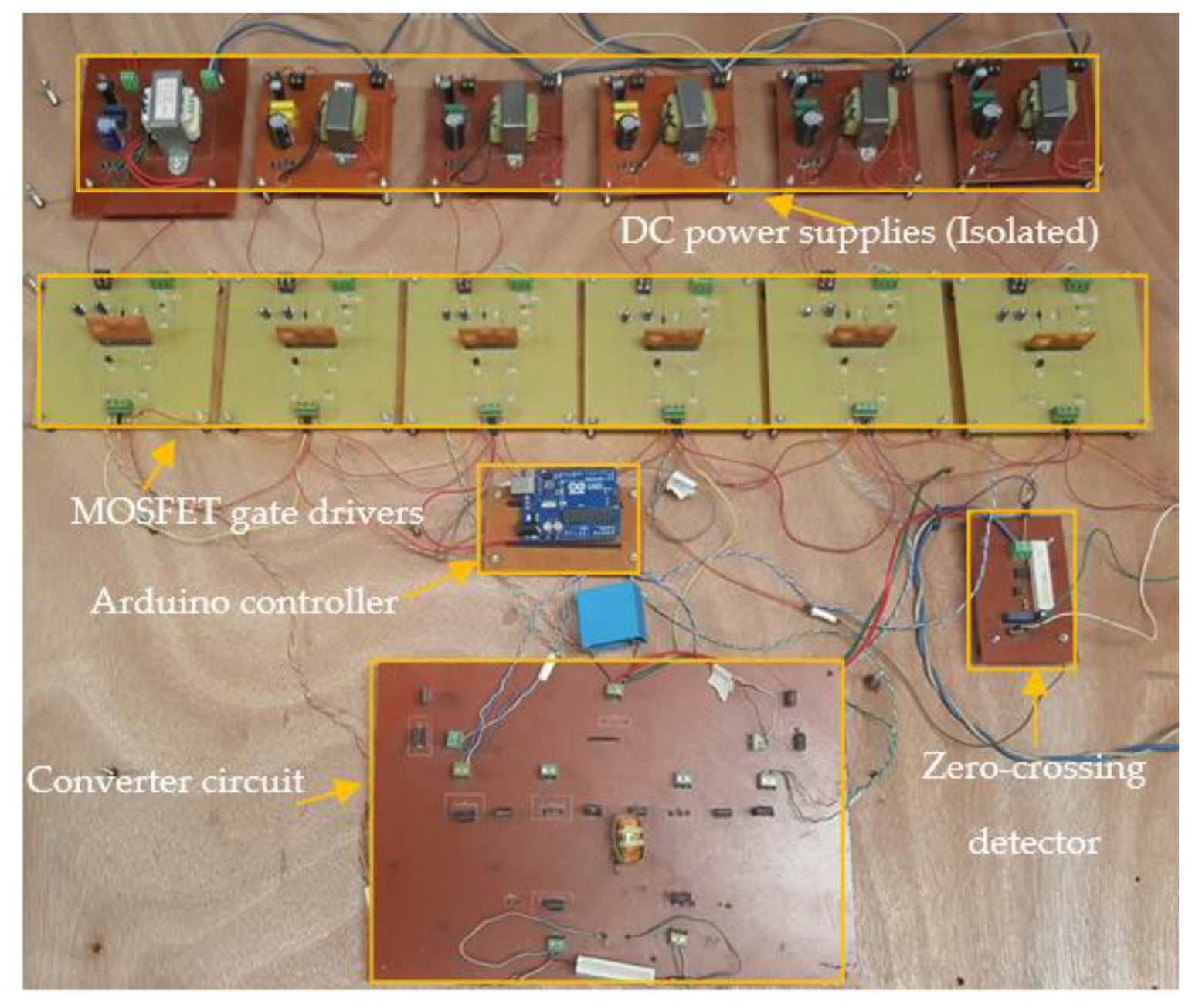
Figure 2 presents the schematic of the developed topology which is structurally quite similar to the one presented by the same authors in [
22]. However, the proposed topology is being used for both low and high-frequency outputs here. It is also being employed for the output voltage regulation by using various voltage control schemes. The unwanted components or fluctuation in the supplied voltage are tackled with the help of input capacitor “
Cin.” The role of the inductor “
L” at the intermediate stage is to tackle the possible shoot-through challenge once controlled switching units operating in complementary mode remain due to practical constraints. Six MOSFETs are selected as switching units to have the advantage of their high switching characteristics. The series-connected diodes with the controlled switching units “
Q1” to “
Q4” can tackle the reverse recovery issue of their body diodes by blocking their currents. These diodes also help to simplify the switching mechanism and facilitates to increase boost factor in output frequency boost operation. There is no such issue for the controlled switching units “
Q5” and “
Q6” connected to the output side. So, there is no need to employ series diodes. The diodes “
D5” and “
D6” connected toward the input side, detect the polarity of the input voltage and becomes forward biased during the positive and negative input voltage respectively. The detail about the governance of the issue of shoot-through is discussed in the next section.
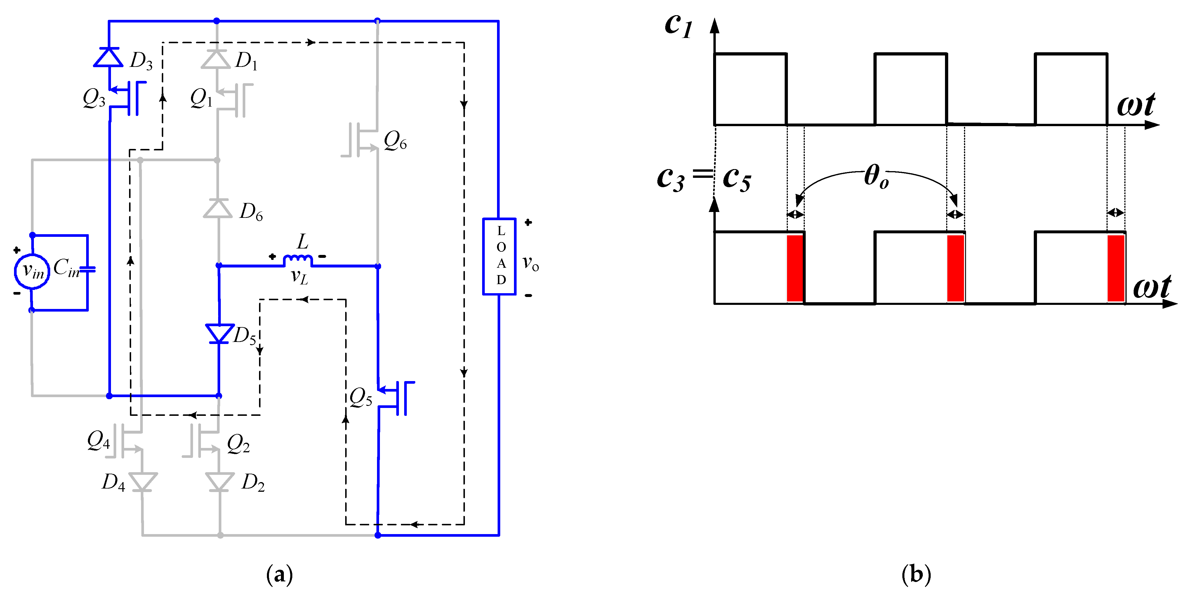
2.1. Shoot through Elimination
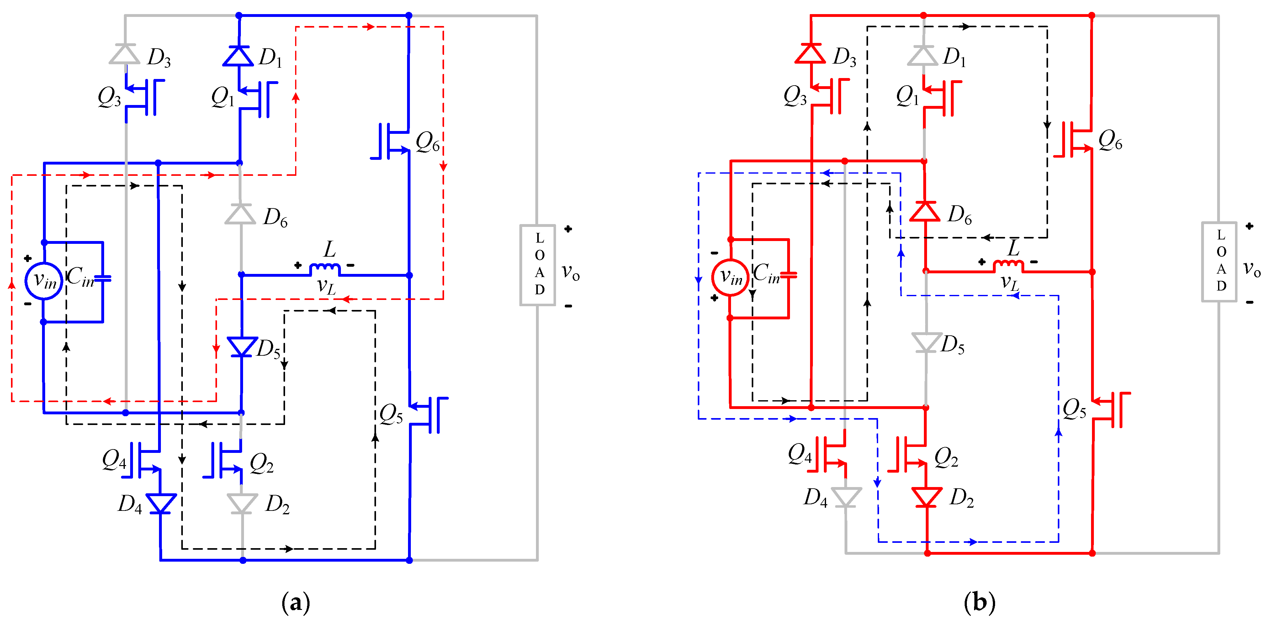
The polarity of the input voltage has an effect on its operation as well as on the output voltage gain. Therefore, the operating behavior during shoot-through intervals is discussed with respect to the polarity of the input voltage. The elimination of the shoot-through during the positive and negative inputs once all the controlled switching units are on is demonstrated with the help of all possible current loops in
Figure 3a,b respectively.
The cathodes of the diodes “
D1”, “
D3” and “
D2”, “
D4” are connected to the same node so their cathode potentials are equal. In this scenario, the diode will conduct the current if its anode voltage is greater than the anode voltage of the other diode that is cathode connected with the cathode of the first one. For example, operation during the positive input as shown in
Figure 3a, the anode terminals of the diodes “
D1”, “
D4” and “
D3” “
D2” are connected to positive and negative terminal of the source respectively. In this case, the diodes “
D1” and “
D4” operate in forward biased mode and corresponding current loops are depicted in
Figure 3a. In the same way, the anode voltage of the diodes
D2,
D3 and
D1,
D4 are positive and negative respectively as can be seen in
Figure 3b. In this condition, the diodes “
D1” and “
D4” cannot conduct and the currents loops shown in
Figure 3b are owing to the conduction of diodes “
D2” and “
D3.” It can also be viewed in
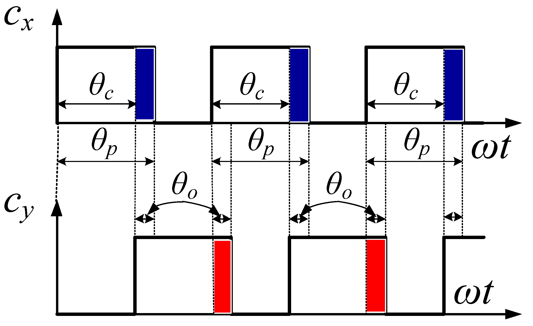
Figure 3 that there are always two current conduction loops during the shoot-through periods that ensure the non-interruption of the inductive current. This characteristic also reduces the current rating of the semiconductor devices during shoot-through intervals. Another point can be viewed that among the six controlled switching units, there are two groups of switching transistors with three transistors in each group. The transistors of each group require the same control signal so any operating mode of the proposed topology can be realized with two switching signals only.
By nature, these signals are complementary and a turn-off delay angle or shoot-through angle (
θo) ensures the safe operation by resolving the inductor current interruption challenge as depicted in
Figure 4. The proper value of this delay can also be used to adjust the boost factor (
β) in high output frequency operation as well. In this interval, the voltage across the intermediate inductor can be calculated in Equation (1) by ignoring the voltage drops in the controlled and uncontrolled switching units.
Similarly, the inductor voltage during the non-shoot through angle is formulated as,
The dc or average value of the inductor voltage during a conduction angle (
θp) is obtained by using Equations (1) and (2).
That may be reduced to the following equation.
For low output frequency, the value of the overlapping or shoot-through angle is not comparable to the non-overlapping angle, so in those cases, the voltage gain or boost factor is approximately unity. Practically it may be less than unity due to voltage drops in the switching units. The boosting characteristics can only be achieved for some limited outputs. So, the basic role of the turn-off delay angle is to avoid the challenge of inductive voltage kicks that may be developed due to inductor current interruption.
2.2. Operating States
Various outputs can be produced from any power-converting topology if its output voltage has inverting and non-inverting characteristics for both polarities of the input voltage. Therefore, investigation of the proposed topology is explored with respect to its non-inverting, inverting, and zero-state with respect to the positive and negative input voltage.
2.2.1. Non-Inverting State
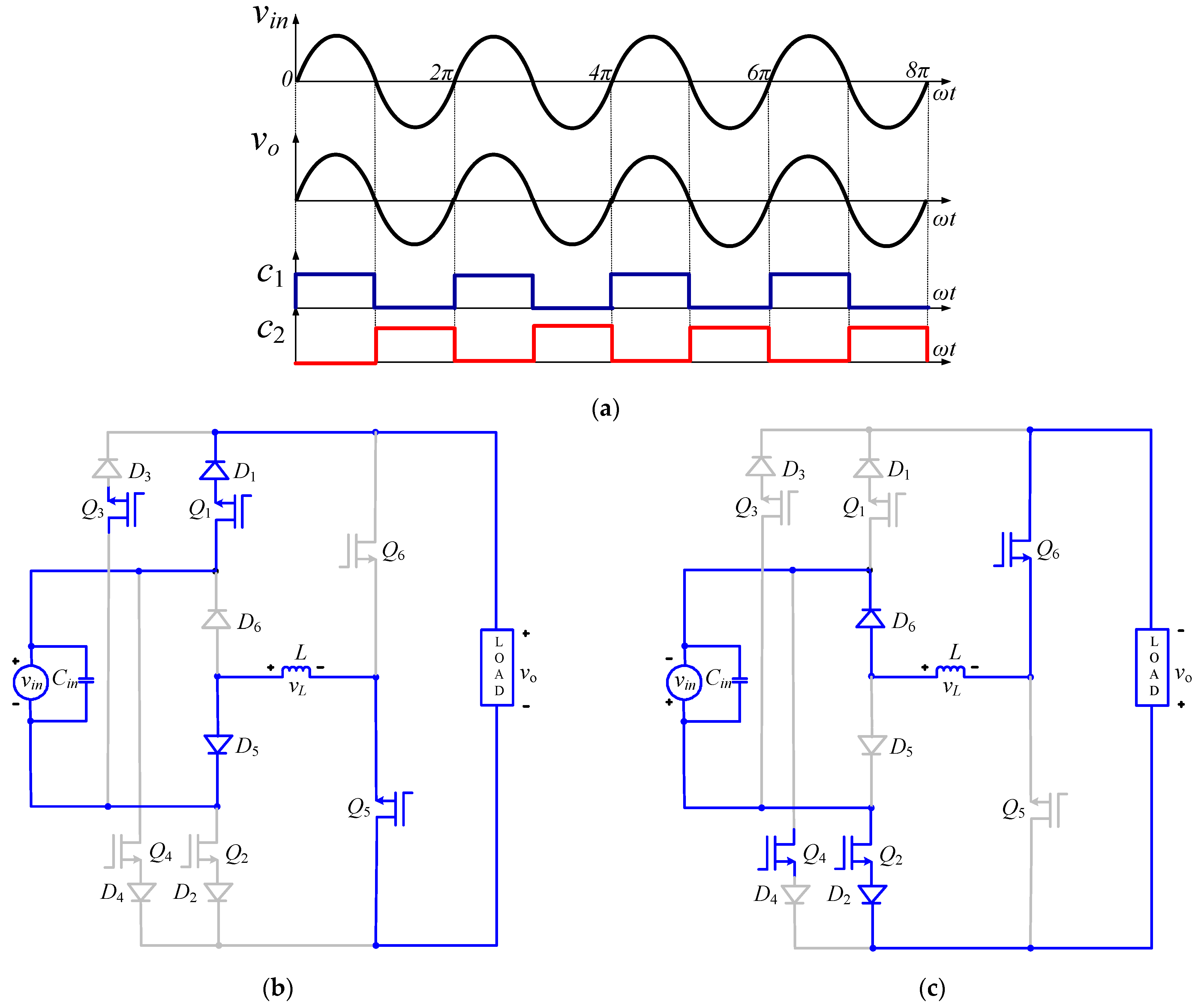
During this state, the boost factor (β) or voltage transfer ratio is always positive ensuring that output and input voltages have the same phase. It means the output voltage is positive and negative if the input voltage is positive and negative respectively. This sort of output is ensured just by connecting the load with input with any polarity of the input voltage. The switching arrangement to achieve this target can be viewed in
Figure 5a that demonstrates how the controlled switching units are turned on and off to achieve this target. The controlled switching units
Q1,
Q3, and
Q5 are turned on and off with the same type of control signal
c1 (
c1 =
c3 =
c5), and the switching control of
Q2,
Q4, and
Q6 is ensured through
c2 (
c2 =
c4 =
c6). Although, in equal phase operation, there is no need to turn on the controlled switching units
Q3 and
Q4. But their control terminals are connected to switching signals to simplify the control algorithm. Their conduction is blocked by reverse biasing their series-connected diodes as their anode is connected to negative polarity during the positive and negative value of the input respectively. The current closed loops of
Figure 5b,c highlight the connection of the load to the source to ensure the voltage in phase operation that is to say.
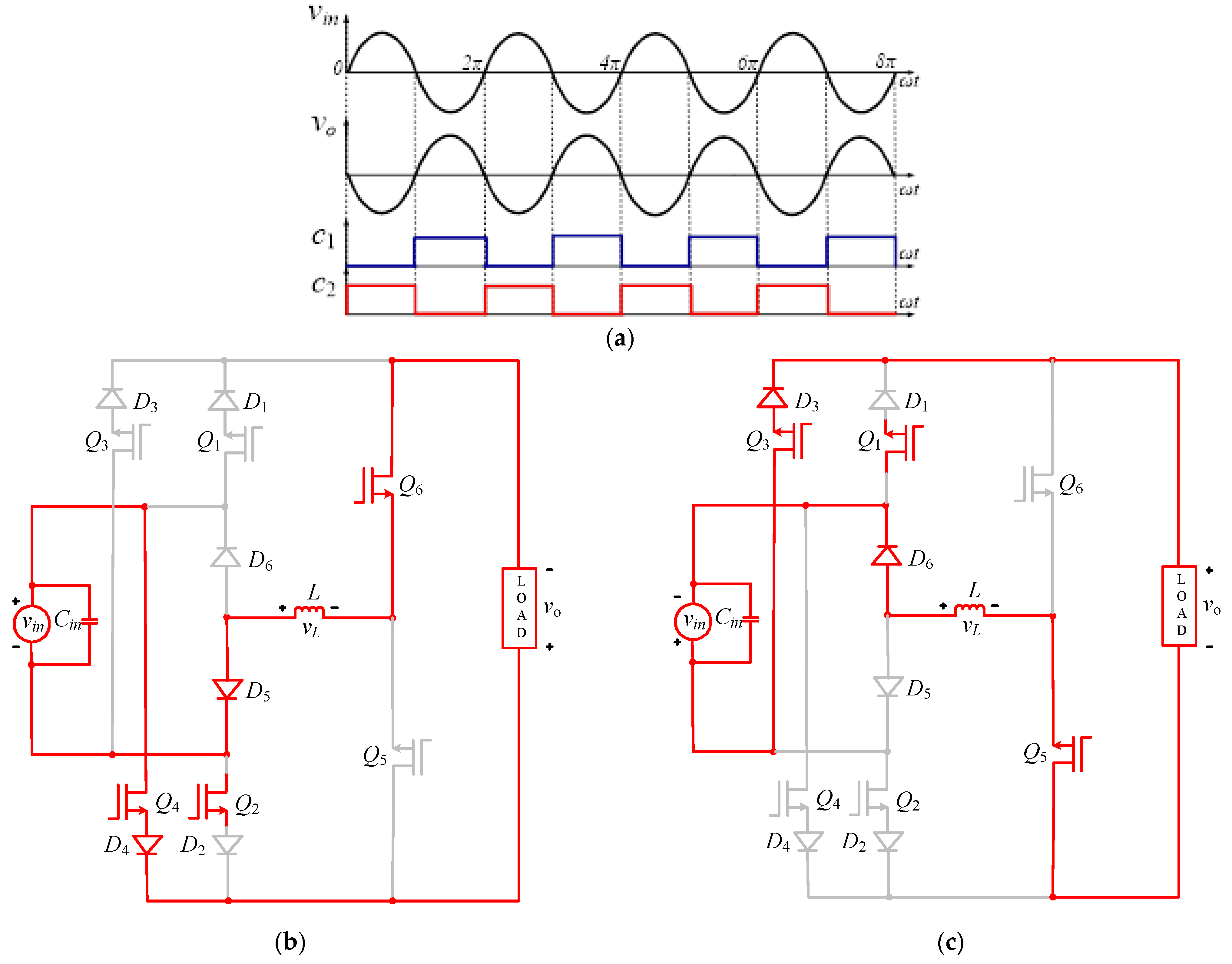
2.2.2. Inverting State
The operation during this state ensures inverting characteristics of the output voltage with respect to the input voltage. It means that output voltage will be negative and positive during the intervals in which the input voltage is positive and negative respectively. The gating signals to control the switching states of the controlled switching units are shown in
Figure 6a. Here it can be viewed that their characteristics are reversed as compared with the switching signals of the non-inverting mode. Also, the operating states of the controlled switching units
Q1,
Q3,
Q5 and
Q2,
Q4,
Q6 are governed from gating signals
c1(
c1 =
c3 =
c5) and
c2 (
c2 =
c4 =
c6). The controlled switching units
Q1 and
Q2 are although on but their conducted current ensured zero by reverse biasing their series-connected diodes
D1 and
D2 as their anode are connected to the negative input voltage during its positive and negative values respectively. The closed current loops of
Figure 6b,c ensure inverting outputs for any polarity of the input voltage and validate the negative voltage transfer ratio or boosting factor. This behavior of the circuit can be modeled by ignoring the internal voltage drops of the switching devices and the intermediate inductor.
2.2.3. Zero-State
This operating state is very critical due to the presence of an inductor at the intermediate state. Its presence ensures the elimination of the possible shoot-through caused by the turning on of the complementary controlled switching units. The sudden interruption of the inductor current takes place once the output is forced to change from non-inverting or inverting to zero; this change of the output at non-zero input voltage leads to the induction of the voltage or current surges that may damage switching devices. The output voltage is zero if all the controlled switching units are maintained in their off state. This is only possible if the intermediate inductor is completely de-energized. This is ensured by adding extra turn-off delays in the controlled switching units that are not directly connected to the input source. For example, during the non-inverting state of positive input voltage as illustrated in
Figure 5b, the controlled switching units
Q1 and
Q5 are conducting to connect load with the source. In this state, although the controlled switch
S3 is on, this branch is in the non-conducting state as its series-connected diode is reverse biased. The issue of inductor current interruption is resolved by adding the turn-off delays (
θo) in gating signals connected to control switching units
Q3 and
Q5. With this arrangement of the switching signals, the controlled switch
Q1 turns off before the turning off of the controlled switches
Q3 and
Q5. This arrangement avoids the current interruption problem of the inductor safely. Then all switching devices maintain their off states to have zero voltage at the output according to the requirement. The closed current loop with corresponding gating signals during the operation in which the output changed from non-inverting to zero-state is illustrated in
Figure 7a,b respectively. A similar approach is considered a non-inverting state for negative input and inverting state both for positive and negative input voltage. The output during this state is realized as
2.3. Output Voltage and Frequency Control
The regulation in the load voltage and frequency may be ensured with the help of the zero, inverting, and non-inverting states of the proposed topology. Various techniques to regulate the output voltage are discussed below.
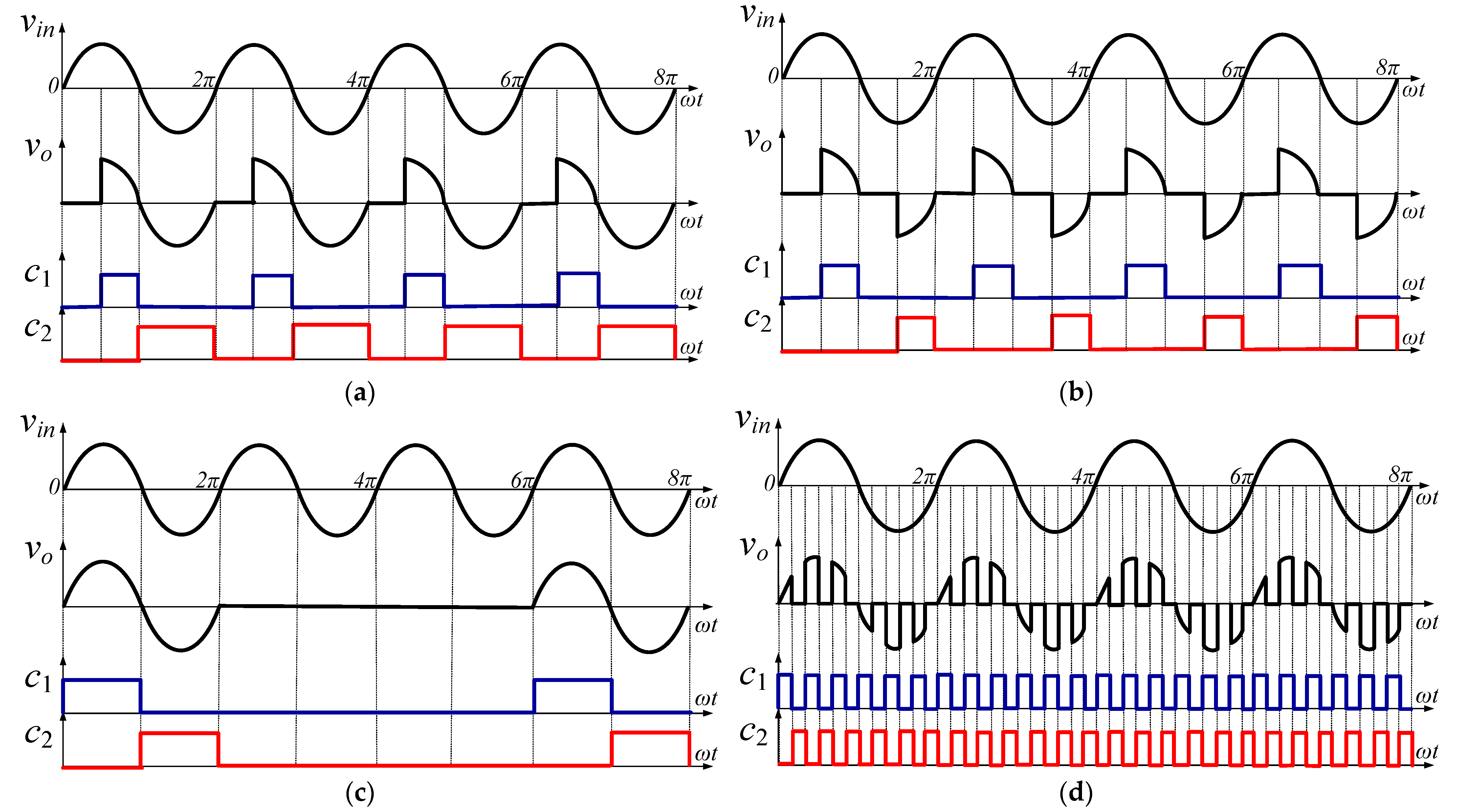
2.3.1. Output Voltage Control
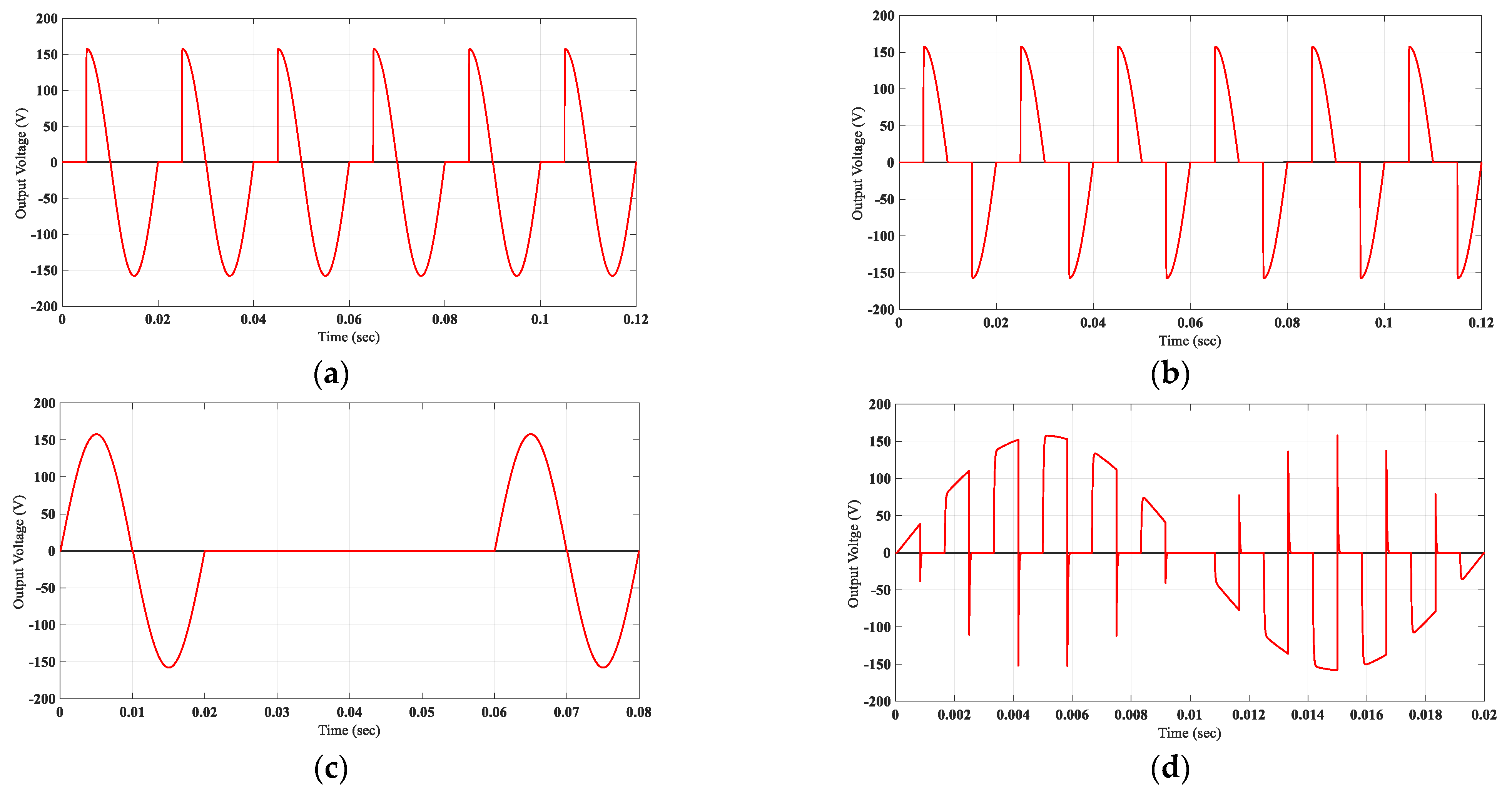
In this control, the RMS value of the output voltage is controlled at a constant standard frequency. There are various voltage control techniques including phase angle (half and full-wave control), on-off cycle control, and PWM chopping. Their switching controls are depicted in
Figure 8 with respect to the input-output voltage waveforms. The output of the half-wave controller as shown in
Figure 8a is obtained by operating the developed topology in zero and non-inverting states respectively during the first quarter and reset cycle of the input voltage.
The symmetrical output of
Figure 8b can be achieved by alternating operating the converter in zero-state and non-inverting state in each half cycle of the input voltage. The output for the on-off cycle control as depicted in
Figure 8c may be realized with the non-inverting and zero-state for one and two input cycles respectively. The behavior of the instantaneous output voltage waveforms of
Figure 8a–c are mathematically explored in Equations (8) to (10) respectively.
Similarly, the PWM chopping in the output voltage can be ensured by alternate operation in non-inverting and zero states and it can be viewed from
Figure 8d.
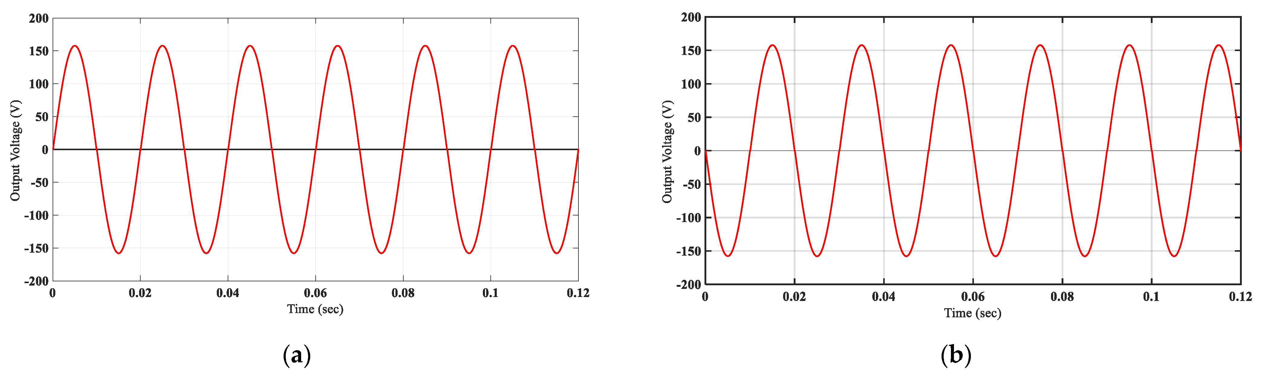
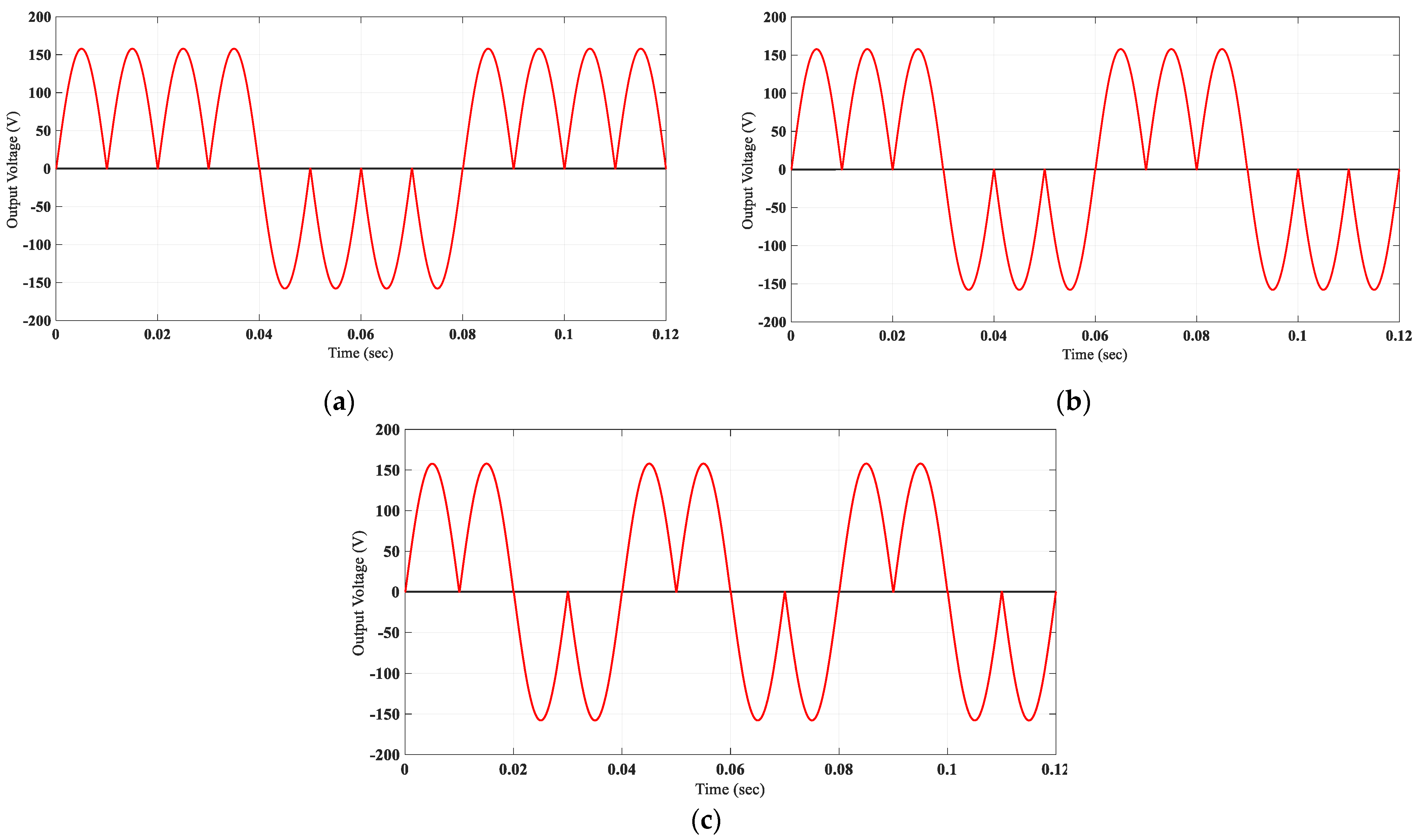
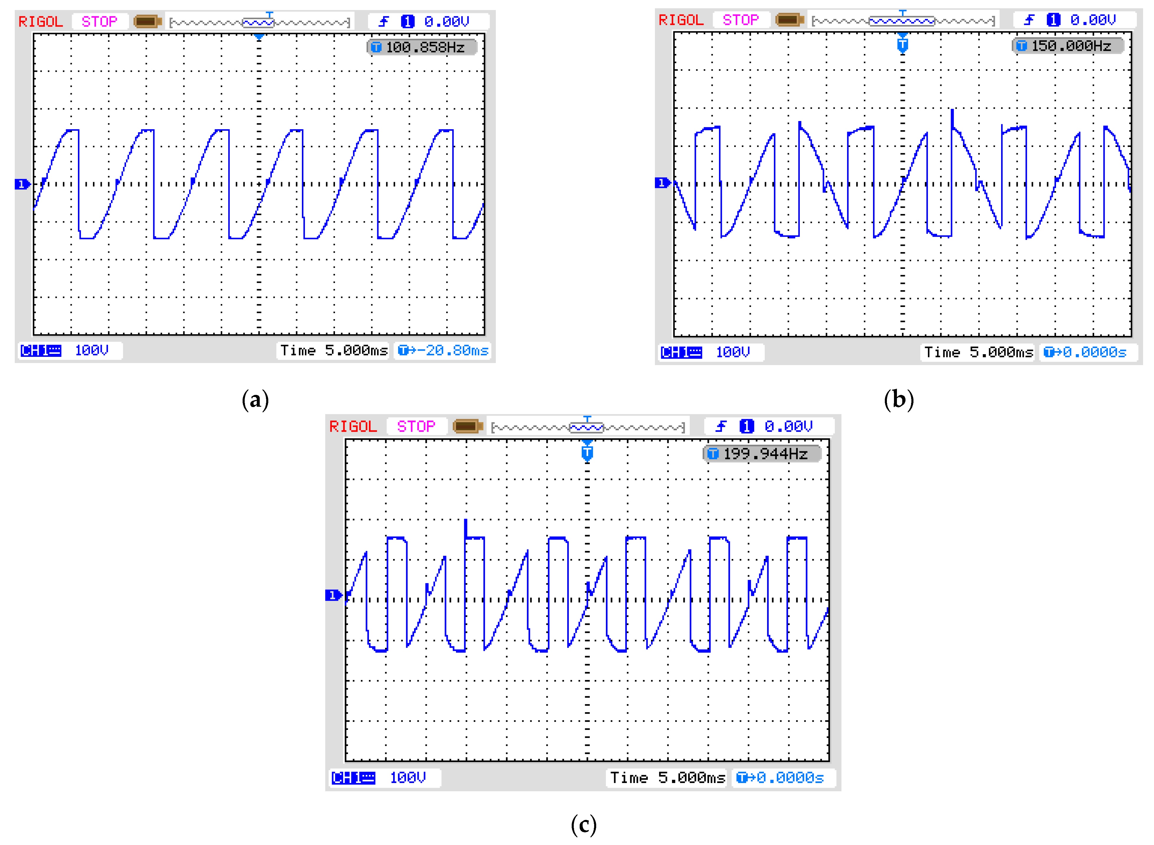
2.3.2. Output Frequency Control
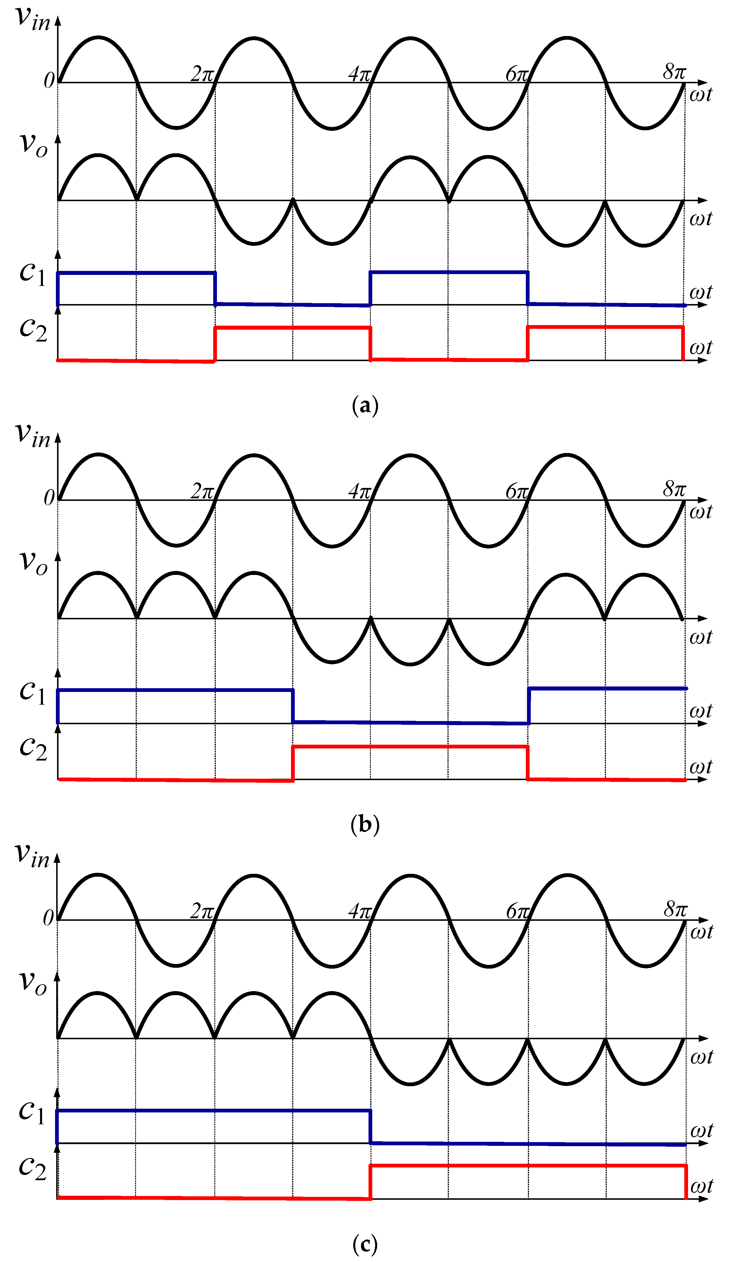
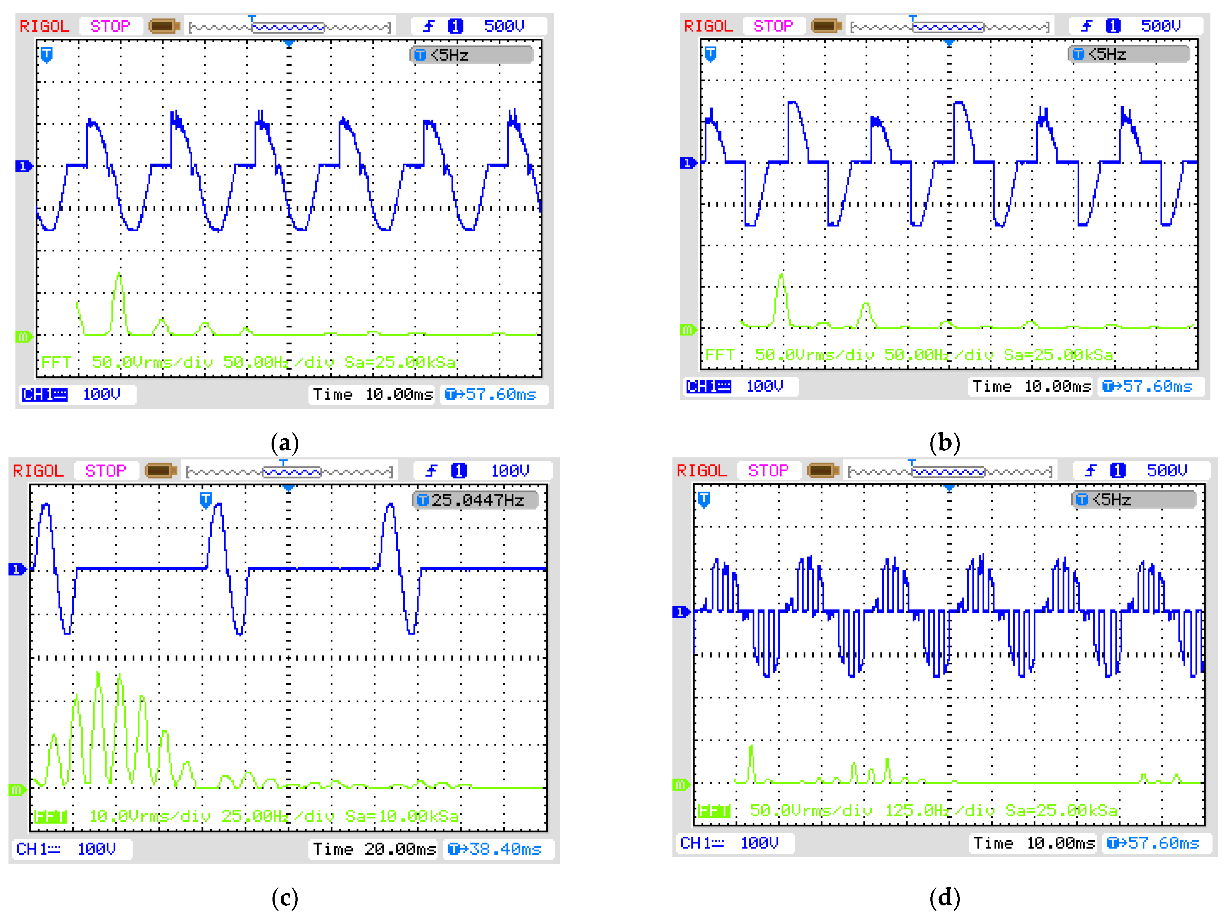
The output frequency regulation in discrete steps can be achieved by operating the proposed topology in non-inverting and inverting states according to the requirements.
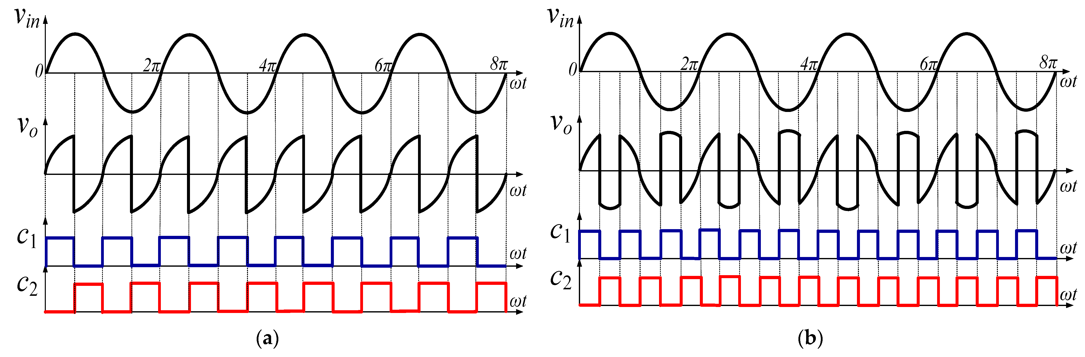
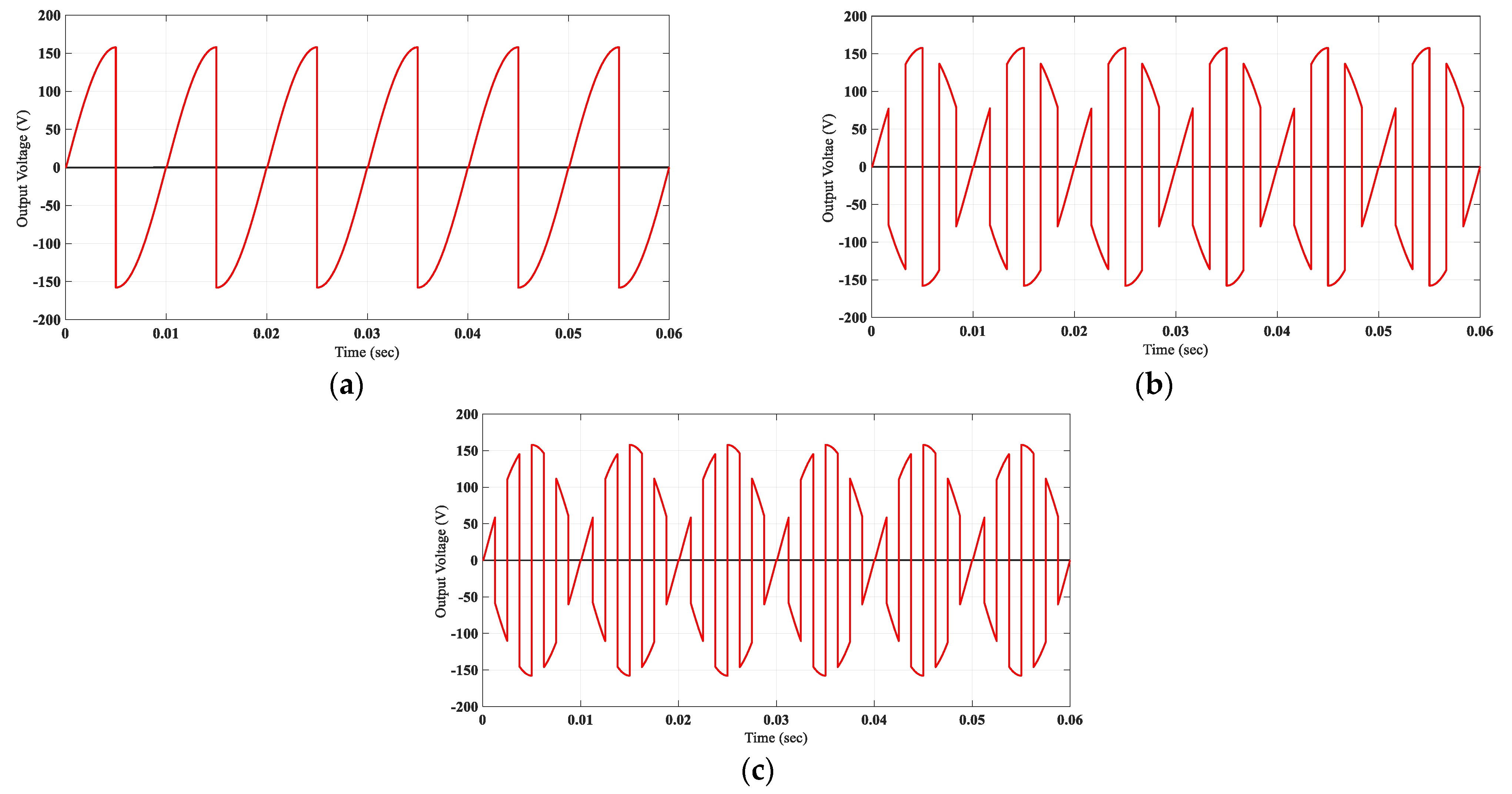
Figure 9 and
Figure 10 depict the gating control schemes for output frequency regulation realized in buck and boost mode respectively.
In
Figure 9a–c, the frequency at the output is controlled to one-half, one-third, and one-fourth of the input respectively. The required outputs can be realized by forcing the developed circuit to operate in non-inverting and inverting states. These characteristics are ensured by setting the control signals
c1 and
c2 to logic high for the first and second half intervals of the output voltage. The instantaneous characteristics of the output voltage waveforms of
Figure 9a–c can be mathematically realized in Equations (11) to (13) respectively.
The same control algorithm can also be employed for frequency step-up operation.
Figure 10a,b shows the gating schemes to have output frequency two and three times the input frequency. For example, for the two-time output frequency realization as shown in
Figure 10a, the output voltage in phase and out phase in every half cycle of the input voltage. While in the case of tree time output frequency, the voltage at the output is non-inverted and inverted two and one-time respectively in each half cycle of the input voltage.
The control input
c1 is logic high once we require non-inverted input at the output while to invert the input, the control input
c2 has to be set to logic high. The nature of the instantaneous output voltage of
Figure 10a,b with the reference of the input voltage is mathematically depicted in Equations (14) and (15) respectively.
Negative and positive values of the instantaneous output voltage illustrate inverting and non-inverting operations.
3. Performance-Wise Comparison with Existing Topologies
The attractive features of the suggested topology may also be validated by comparing its characteristics with the existing converter as in [
24] employed to have similar outputs. The transformer-less implementation is one of the major achievements of the proposed topology. This not only reduces the overall size and cost but also reduces the conversion losses as core losses are more significant than the losses caused by the semiconductor devices. The center tap transformer that is an integral part of the multi-converter reported in [
24], is employed for multiple outputs. The flow of unidirectional and low-frequency current is a big issue in this type of transformer compared to a two-winding transformer. These currents normally cause the core saturation issue. The absence of an intermediate inductor in [
24] may cause the shoot-through issue and switching devices may damage due to the flow of excessive current during these intervals.
The performance of the AC-AC converters may be evaluated in terms of a maximum breakover voltage (
Vbr) for the switching devices, switching or chopping voltage (
Vch) and currents (
Ich), power factor (
PF), harmonic factor (
HF), switching (
PS), and conduction losses (
PC) as performance index parameters. The maximum breakover voltage that can be developed across the switching devices in the proposed architecture is limited only to the peak value of input voltage (
Vm). The architecture of the converter [
24] is implemented with a center tap transformer having two secondary windings. At any time instance, if switching devices of one secondary winding are conducting then switching elements of the other secondary winding remain in non-conducting. The maximum breakover voltage of the switching devices in this architecture is the sum of the peak voltage of the two secondary (output) windings. The same is true for the switching or chopping voltage. Therefore, the maximum breakover and switching voltage of the converter architecture in [
24] is double that of the developed architecture, i.e.,
The power conversion losses of the suggested architecture include only the switching (
PS) and conduction (
PC) losses of operating transistors and diodes. The switching losses of the fast recovery diode can be ignored due to the low value of the reverse current and reverse recovery time. These losses for one transistor and diode are computed as.
Here, IS is the steady-state current conducted by the switching devices, fch is switching or chopping frequency, and tr and tf are the rise and fall times of the switching transistors. RT(on) is the internal resistance of the transistor during its on-state. In the same way, RD(on) and VD(on) are the on-state resistance and voltage of the forward-biased diode respectively.
The harmonic coefficients of the input current are computed to determine the power quality of the input current by computing the harmonic and power factor. They are computed with the total RMS value of the input current (
Iin), input RMS current at the fundamental component (
Iin(1)), and its displacement angle (
). Mathematically, they are computed as
Now above-defined performance indices are numerically computed with the 160 V peak value of the input voltage. For calculation purposes, the connected load is assumed resistive. It can be observed that the peak breakover voltage of the switching devices in the proposed topology is 160 V while in [
24], it is 320 V that is almost double. In the same way, the chopping or switching voltage in [
24] is also double. The conversion losses in the suggested architecture only come from the conduction and switching losses while in [
24], along with these losses, core losses contribute much of the conversion losses. In one PWM switching interval, there is a conduction of two transistors and two diodes, so conduction and switching losses of the proposed topology are computed as
Similarly, for the architecture in [
24], there is the conduction of only one transistor and diode, so their switching and conduction losses are calculated as,
The switching losses of both architectures are the same although there is a switching of one transistor in [
24] instead of two as in the suggested topology. This is due to the double chopping voltage. But the conduction losses of the power converting architecture in [
24] is almost half if equal internal voltage and resistance of the switching devices are considered. But practically, these values increase with an increase in the maximum breakover and chopping voltage. It has already been pointed out that the cost and conversion losses of the suggested architecture are low due to the absence of a low-frequency transformer.
As far as the power quality is concerned, the input current in the suggested architecture is non-distorted; its power factor is high and the harmonic factor is low. But the power converting architecture reported in [
24] has two secondary windings and each secondary winding is connected in series with the diode, transistor, and load. Hence it behaves as a half-wave rectifier circuit. With these characteristics, the input current of each secondary of the transformer is distorted and contains unwanted harmonics including dc component–one of the major power quality issues. This component not only contributes to the power losses but also leads to the undesirable core saturation issue. With Fourier theory, the input dc, RMS, RMS current at the required frequency and its displacement angle is computed as
Here
Im is the peak value of the output or input current. It can be noted here that the dc component in the input current is compared to the total input RMS current. The numerical value of the dc component is also greater than the RMS value of the required current component. So, this component increases the core saturation potency with heavy-duty loads. With these values, the power and harmonic factor of each secondary is calculated as
The comparison of the suggested converter and power converting topology in [
24] in terms of performance indices with resistive load is also explored in
Table 1.
In summary, there is no problem with core saturation and core losses as the developed topology needs not to employ the input transformer. The intermediate inductor ensures the elimination of the shoot-through issue. The current interruption problem of the inductor is tackled by establishing two current loops in each operating mode. The developed topology may be attractive to produce multiple types of output with simplified switching schemes. Along with this, the maximum breakover and switching voltage and harmonic factor are low and the power factor is improved. These attractive features increase its workability over the converter in [
24].


