Article

Fabrication of Large Area, Ordered Nanoporous Structures on Various Substrates for Potential Electro-Optic Applications

1
Department of Electrical and Computer Engineering, Sungkyunkwan University, Suwon 16419, Korea
2
Smart Energy & Nano R&D Group, Korea Institute of Industrial Technology, Gwangju 61012, Korea
*
Author to whom correspondence should be addressed.
Appl. Sci. 2021, 11(24), 12136; https://doi.org/10.3390/app112412136
Submission received: 31 October 2021 / Revised: 10 December 2021 / Accepted: 15 December 2021 / Published: 20 December 2021
(This article belongs to the Special Issue Active Nano Optics)

Abstract

:
Nanoporous structures have attracted great attention in electronics, sensor and storage devices, and photonics because of their large surface area, large volume to surface ratio, and potential for high-sensitivity sensor applications. Normally, electron or ion beam patterning can be used for nanopores fabrication by direct writing. However, direct writing is a rather expensive and time-consuming method due to its serial nature. Therefore, it may not translate to a preferred manufacturing process. In this research, a perfectly ordered large-area periodic pattern in an area of approximately 1 cm2 has been successfully fabricated on various substrates including glass, silicon, and polydimethylsiloxane, using a two-step process comprising visible light-based multibeam interference lithography and subsequent pattern transfer processes of reactive ion etching and nanomolding. Additionally, the multibeam interference lithography templated anodized aluminum oxide process has been described. Since the fabrication area in multibeam interference lithography can be extended by using a larger beam size, it is highly cost effective and manufacturable. Furthermore, although not described here, an electrodeposition process can be utilized as a pattern transfer process. This large-area perfectly ordered nanopore array will be very useful for high-density electronic memory and photonic bandgap and metamaterial applications.

1. Introduction

Because of their large surface area, large volume to surface ratio, and potential for high sensitivity sensor applications, nanoporous structures have drawn great attention in electronics, sensor and storage devices, and photonics [1,2,3,4,5,6]. Electron or ion beam patterning can be used for nanopore fabrication by direct writing [7,8,9,10]. However, direct writing is a rather expensive and time-consuming method due to its serial nature. Therefore, it may not translate to a preferred manufacturing process. Meantime, metal anodization processes, i.e., anodized aluminum oxide (AAO) and anodized titanium oxide (ATO) processes, are used for large-area nanopore templates [11,12,13,14], but their array patterns tend to contain locally disordered portions, which would limit their usage for electronic memory devices or photonic devices requiring perfectly ordered arrays over a large area. Multibeam interference lithography (MIL), however, could be a good candidate for the patterning of perfectly ordered large-area photonic crystals and can be applied for photonic, electronic applications [15,16,17,18,19]. MIL can form interference patterns on photosensitive polymer. In our previous work, MIL and two-photon lithography were combined by two-step exposures and a single development process. This new approach, adding patterns on the repeated nanoporous structures, suggested a new path from restricted usages of nanoporous structures to various applications but essentially, the newly fabricated structures were still made of the same material, polymer, and there was a limit to their usage for diverse applications [20]. To overcome its limitations and construct a functional electronic or photonic device, pattern transfer to the underneath layers or substrates is required.
In this work, three-beam interference lithography with a visible light source is used to form hexagonal symmetric interference patterns on a large photoresist (PR) layer. Subsequently, various pattern transfer processes to different substrates such as reactive ion etching (RIE) to glass and Si substrates, nanomolding to a polydimethylsiloxane (PDMS) substrate, and anodization to an aluminum-coated substrate were performed. By combining MIL and RIE/nanomolding, nanoporous polymer structures could be transferred to various substrates and this can provide the opportunity to be used for a variety of applications for electronic and photonic devices.

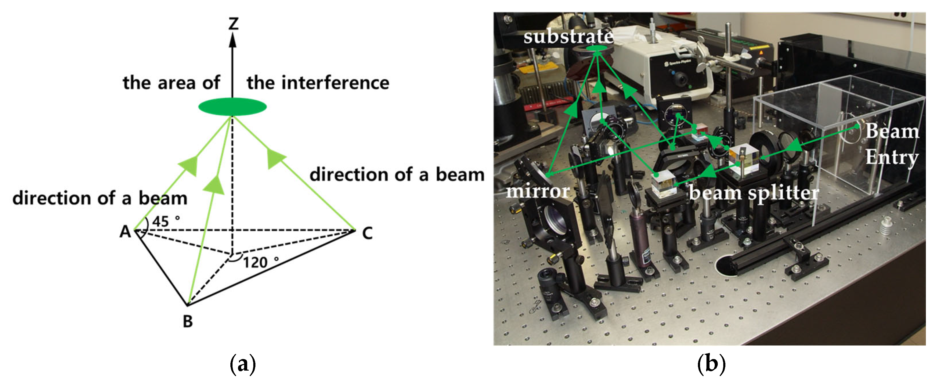
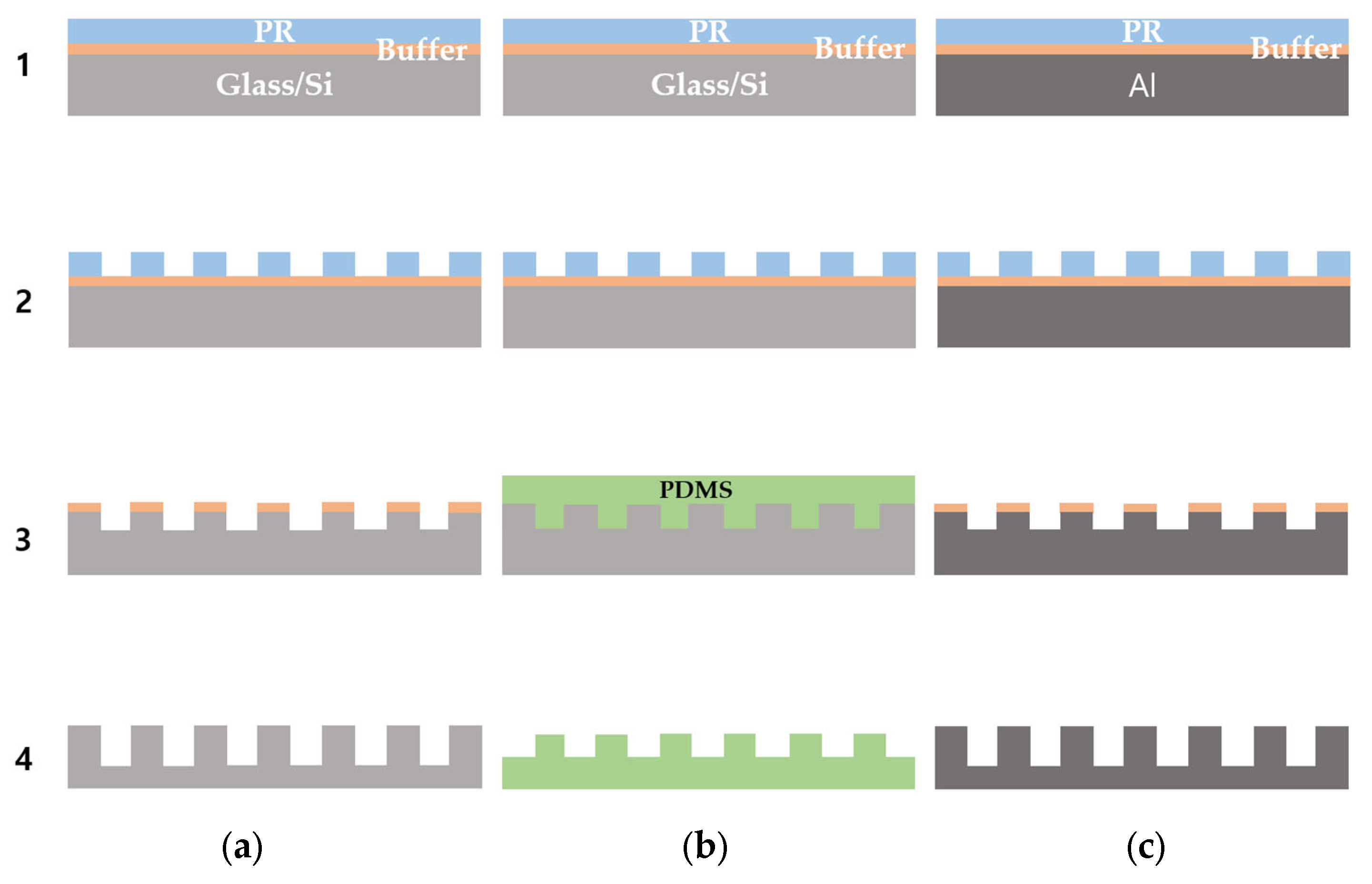
2. Materials and Methods

To fabricate nanoporous structures with a large area, multibeam interference lithography was performed using a cw Nd:YVO4 laser (Verdi V6, Coherent, Palo Alto, CA, USA) with a wavelength of 532 nm. The whole covered area by MIL was approximately 1 cm2 and the covered area can be adjusted by varying the aperture size of the beam. As PR, Epon SU-8 (Miller-Stephenson Chemical, Inc., Sylmar, CA, USA) was selected due to its good solubility and transparency in visible and UV light. The SU-8 was doped with a photosensitizer, Rubrene (Sigma-Aldrich, Inc., Burlington, MA, USA) and a photoacid generator, diaryliodonium hexafluoroantimonate (PC-2506, Polyset, Mechanicville, NY, USA) to respond to the green laser. Figure 1 shows the experimental setup and a schematic of three-beam interference lithography where the incident angle of each beam was 45° from the vertical line, and the phase difference was 120° between beams in the horizontal plane. Depending on the phase angle of each incident beam and the PR type, either a hexagonal symmetric nanopore array or a nanopillar array was formed.
Figure 2 shows the nanoporous structures on the substrate fabricated by MIL. As is shown, well-ordered interference patterns were fabricated, which covered 1 cm2. Depending on the optical property of the substrate, a buffer layer was used between the substrate and the photopatterning layer to minimize the reflection.

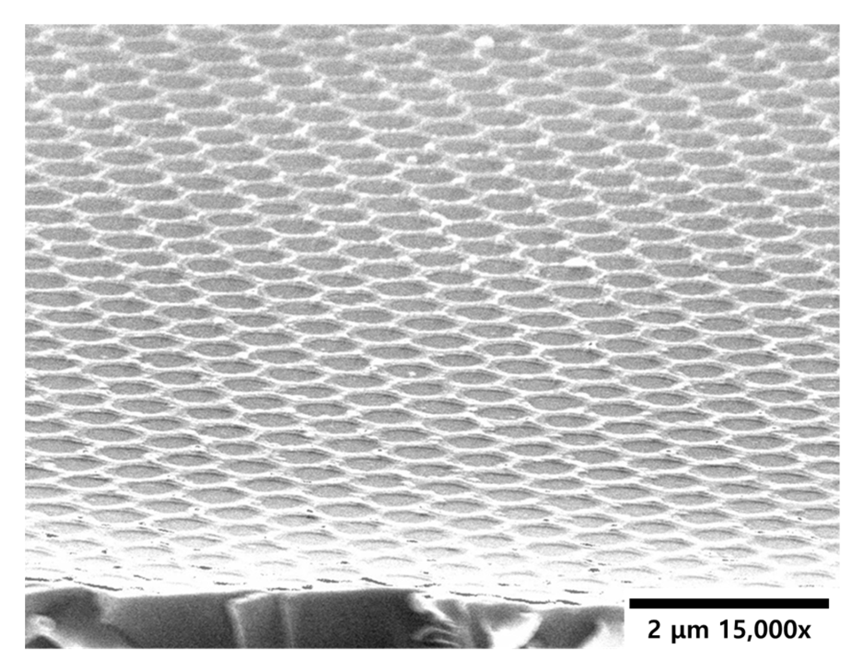
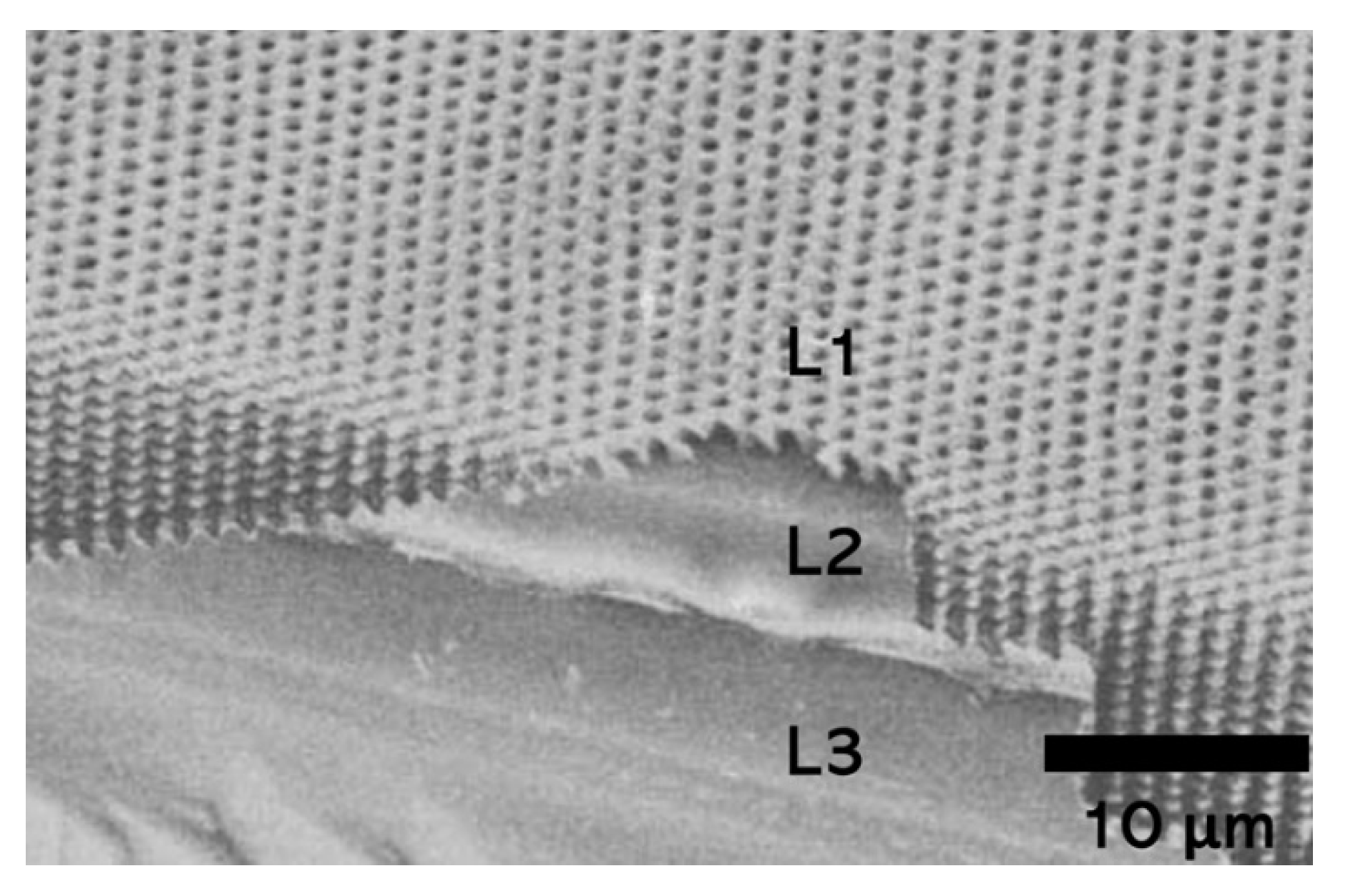
3. Results and Discussion

As pattern transfer methods, three different approaches are shown in Figure 3. Figure 3a used a (RIE) process for a pattern transfer method to a Si or glass substrate. When glass is used as a substrate, the buffer layer between the PR and the substrate may not be critical since the refractive index difference between SU-8 (n = 1.59) and glass (n = 1.50) is relatively small and no significant portion of optical dose is reflected to generate parasitic patterns. On the other hand, when Si is used, reflection between SU-8 and Si (n = 3.42) would be quite significant due to its large refractive index difference, and the buffer layer design becomes very critical. SU-8 doped with Rhodamine B (RhB) dye (Sigma-Aldrich, Inc., Burlington, MA, USA) has been used because of its strong absorption of green light and high quantum efficiency. First, RhB was dissolved in cyclopentanone and mixed with SU-8 and photoacid generator, where the weight ratio of SU-8:RhB:PC was 10:0.1:1. It was spin-coated on a polished Si substrate at 2000 rpm for 40 s. After soft baking it on a hotplate at 95 °C for a minute, it was flood-exposed under the multiband UV light for one minute and hard baked at 160 °C for 10 min. The resultant thickness was approximately 2.5 μm. Next, a SU-8 PR layer with a weight ratio of SU-8:Rubrene:PC of 100:0.2:2.5 was spin-coated at 4000 rpm for 40 s, followed by soft baking at 95 °C for a minute (Figure 3(a1)). Three-beam interference lithography was performed on a circular exposure area with a diameter of 1 cm. The cumulative intensity of the exposure energy was 0.6 W cm−2 and exposed beams for 3 to 8 sec gave the total exposure dosage for 2 to 5 J cm−2. When the incident beams reached the PR layer, which has very good thermal stability, the exposed areas increased in molecular weight and photochemically transformed to form insoluble products [21]. The specimen was post baked on a hot plate at 95 °C for a minute and cooled down to room temperature, followed by development in propylene glycol monomethyl ether acetate (PGMEA). The thickness was approximately 300–400 nm (Figure 3(a2)). RIE was performed in an oxygen-dominant environment for buffer layer patterning (Figure 3(a3)) and in a chlorine-dominant environment for Si layer patterning (Figure 3(a4)). Figure 4 shows a fabricated photonic crystal membrane at the stage depicted in Figure 3(a2).
The three layers are clearly seen with the top layer patterned in a hexagonal symmetric shape. Figure 5 shows a pattern transferred glass substrate, where RIE has been performed in O2:CF4 of 15:3.5 sccm with a power of 20 W for 30 s for buffer layer etching and in O2:CH4 of 5:40 sccm with 70 W for 2 min for glass etching [13]. Figure 3b shows a pattern transfer process using polydimethylsiloxane (PDMS) nanomolding. After the interference lithography and RIE process with PR on the glass substrate to make nanoporous glass structures as shown in Figure 3a, PDMS was poured on the nanoporous glass surface and cured at 60 °C for 2 h. After cooling down to room temperature, a nanopillar array, which is the negative form of the nanopore array, was formed upon separation. Figure 6a is the top view of a perfectly ordered hexagonal symmetric nanopore array, with the inset showing a magnified oblique view. Figure 6b shows a replicated PDMS structure after nanomolding, with the inset showing a magnified view of the pillar array. The scanning electron microscopy image demonstrates good fidelity. The anodized aluminum oxide (AAO) process converts pure aluminum into aluminum oxide in a specific shape, as shown in Figure 7, when it is anodized in an acidic environment under a bias voltage. The pore size and the pitch between pores can be controlled by the magnitude of the bias voltage and the type of acids. For example, the pore pitch is in the range of 50–60 nm at a bias voltage of 19–25 V in sulfuric acid (H2SO4), 220 nm–300 nm at 120–250 V in oxalic acid (H2C2O2), and 405–500 nm at 160–195 V in phosphoric acid (H3PO4). If the bias voltage is lower than the optimal range, pores formed are not well ordered. If the bias voltage is higher than the optimal range, the barrier layer breaks down and substrate burning occurs. Fabricated anodized aluminum oxide layer samples are shown in Figure 8. A two-step AAO process has been used to form more uniform pore sizes. First, aluminum foil undergoes thermal pretreatment at 400 °C for one hour, which forms a thin layer of oxide layer, preventing initial breakdown upon applying bias voltage. The first anodization is performed in oxalic acid at 40 V for 6 min, which gives rise to relatively random pores, as shown in Figure 8a. The first anodized layer is etched away using a solution consisting of 1.8 wt% chromic acid and 6 wt% phosphoric acid for an hour. After etching, small bumps are formed along the barrier depicted in Figure 7. The bumps serve as guides for the second anodization. The second anodization is performed in oxalic acid at 40 V for 4 min. Optionally, pore widening step is performed using 6 wt% phosphoric acid for an hour. Figure 8b,c are the cross-section view and the top view, respectively. The average pore size and the average pitch are 60 nm and 100 nm, respectively [15]. Figure 3c shows a direct pattern transfer onto an aluminum layer using AAO immediately followed by MIL. The anodization is being performed using phosphoric acid at 160 V to have a pore pitch of 500 nm. As an alternative to the direct anodization process after MIL, template-assisted anodization can be used. However, there are some challenges, including reflection and pore size matching issues between one from MIL and one from AAO. In order to preserve the perfect pore ordering from MIL, further work is required.

4. Conclusions

A perfectly ordered large-area periodic pattern in an area of approximately 1 cm2 has been successfully fabricated on various substrates including glass, Si, and PDMS, using a two-step process comprising visible light-based MIL and subsequent pattern transfer processes of RIE and nanomolding. Additionally, the MIL-templated AAO process has been described. Since the fabrication area in MIL can be extended by using a larger beam size, it is highly cost effective and manufacturable. This large-area perfectly ordered nanopore array will be very useful for high-density electronic memory and photonic bandgap and metamaterial applications, sensors, nanolens and photonics [22].

Author Contributions

Conceptualization, H.J.; methodology, H.J. and K.J.; data curation, H.J. and M.-J.P. writing—original draft preparation, H.J.; writing—review and editing, H.J. and J.L.; supervision, J.L. All authors have read and agreed to the published version of the manuscript.

Funding

This work was supported by the Technology Innovation Program funded by the Ministry of Trade, Industry & Energy (MOTIE) of the Republic of Korea. (No. 20010965).

Institutional Review Board Statement

Not applicable.

Informed Consent Statement

Not applicable.

Data Availability Statement

The data that support the findings of this study are available upon reasonable request.

Conflicts of Interest

The authors declare no conflict of interest.

References

  1. Deyang, J.; Tao, L.; Harald, F. Patterning and applications of nanoporous structures in organic electronics. Nano Today 2020, 31, 100843. [Google Scholar]
  2. Huang, Y.G.; Shiota, Y.; Wu, M.Y.; Su, S.Q.; Yao, Z.S.; Kang, S.; Kanegawa, S.; Li, G.-L.; Wu, S.-Q.; Kamachi, T.; et al. Superior thermoelasticity and shape-memory nanopores in a porous supramolecular organic framework. Nat. Commun. 2016, 7, 11564. [Google Scholar] [CrossRef] [PubMed] [Green Version]
  3. Mohsin, A.B.; Jun, K.; Hoyoung, J.; Seok-Min, K. Fabrication of Highly Packed Plasmonic Nanolens Array Using Polymer Nanoimprinted Nanodots for an Enhanced Fluorescence Substrate. Polymers 2018, 10, 649. [Google Scholar]
  4. Li, X.; Shao, J.; Tian, H.; Li, X.; Chen, X.; Zhu, X. High-transmittance and focal controllable plano-convex lenses with embedded nanolens bottoms formed by electrowetting on a colloidal monolayer. J. Mater. Chem. C 2020, 8, 2659–2663. [Google Scholar] [CrossRef]
  5. Junsoo, P.; Changhoon, C. Aluminum based reflective nanolens arrays to improve the effectiveness of ultraviolet inactivation of Escherichia coli O157:H7 and Listeria monocytogenes in water and a sucrose solution. Food Sci. Biotechnol. 2020, 29, 1281–1287. [Google Scholar]
  6. Sergey, A.S.; Alexey, Z.; Dmitri, V.P.; Stanislav, O.G.; Eugeny, V.P.; Alexey, P.P.; Svetlana, N.K.; Sergei, A.K.; John, B.B.R.; Sergey, I.K.; et al. Plasmonic Nanolenses Produced by Cylindrical Vector Beam Printing for Sensing Applications. Sci. Rep. 2019, 9, 19750. [Google Scholar]
  7. Cai, J.; Lv, C.; Hu, C.; Luo, J.; Liu, S.; Song, J.; Shi, Y.; Chen, C.; Zhang, Z.; Ogawa, S.; et al. Laser direct writing of heteroatom-doped porous carbon for high-performance micro-supercapacitors. Energy Storage Mater. 2020, 25, 404–415. [Google Scholar] [CrossRef]
  8. Rebecca, L.W.; Michael, J.B.; Beecher, H.W.; Elizabeth, R.K.; Mark, A.F.; Richard, J.M.; Gery, L.M. Direct writing of textured ceramics using anisotropic nozzles. J. Eur. Ceram. Soc. 2021, 41, 1945–1953. [Google Scholar]
  9. Sergey, G.; Vitaliy, A.G.; Joan, V.-C.; Christian, D. Direct e-beam writing of dense and high aspect ratio nanostructures in thick layers of PMMA for electroplating. Nanotechnology 2010, 21, 295303–295310. [Google Scholar]
  10. Birgitta, S.; Loic, A.; Laurent, B.; Abdelghani, O.; Madouri, A.; Gilles, P.; Juan, P.; Ralf, J.; Jacques, G. Direct FIB fabrication and integration of “single nanopore devices” for the manipulation of macromolecules. Microelectron. Eng. 2010, 87, 1300–1303. [Google Scholar]
  11. Zhang, W.; Tian, Q.; Chen, Z.; Zhao, C.; Chai, H.; Wu, Q.; Li, W.; Chen, X.; Deng, Y.; Song, Y. Arrayed nanopore silver thin films for surface-enhanced Raman scattering. RSC Adv. 2020, 10, 23908–23915. [Google Scholar] [CrossRef]
  12. Alexander, M.H.; Pravini, S.F.; Smilgies, D.M.; Jeffrey, M.M. Freeing Organic Semiconductor Nanowires from Nanoporous Aluminum Oxide Templates: Effects on Morphology, Crystal Structure, and Molecular Aggregation. Cryst. Growth Des. 2021, 21, 721–728. [Google Scholar]
  13. Yu, J.; Wang, F.; Wang, Y.; Gao, H.; Li, J.; Wu, K. Interfacial reaction growth approach to preparing patterned nanomaterials and beyond. Chem. Soc. Rev. 2010, 39, 1513–15325. [Google Scholar] [CrossRef]
  14. Shobha, S.; Kyoung-Tae, K.; Alexander, B.; Natalia, M.L.; Paras, N.P. Fabrication and Characterization of Gold−Polymer Nanocomposite Plasmonic Nanoarrays in a Porous Alumina Template. ACS Nano 2010, 4, 2249–2255. [Google Scholar]
  15. Hu, X.; Zhang, X.; Chen, X.; Luo, M. Solution route to large area all-TiO2 one-dimensional photonic crystals with high reflectivity and different structural colors. Nanotechnology 2020, 31, 135209. [Google Scholar] [CrossRef]
  16. Menaka, D.Z.; Masahiro, Y.; Bongshik, S.; Kenji, I.; Takuya, I.; Shumpei, K.; Koki, I.; Yoshinori, T.; Ranko, H.; John, G.; et al. Thermal management for CW operation of large-area double-lattice photonic-crystal lasers. J. Opt. Soc. Am. B 2020, 37, 3882–3887. [Google Scholar]
  17. Hyuk Moon, J.; Yang, S. Creating Three-Dimensional Polymeric Microstructures by Multi-Beam Interference Lithography. J. Macromol. Sci. C 2005, 45, 351–373. [Google Scholar] [CrossRef] [Green Version]
  18. Woo, L.; Ran, J.; Ulrich, G.; Kornelius, N. Fast fabrication of long-range ordered porous alumina membranes by hard anodization. Nat. Mater. 2006, 5, 741–747. [Google Scholar]
  19. Baquedano, E.; Torné, L.; Caño, P.; Postigo, P.A. Increased Efficiency of Solar Cells Protected by Hydrophobic and Hydrophilic Anti-Reflecting Nanostructured Glasses. Nanomaterials 2017, 7, 437. [Google Scholar] [CrossRef] [PubMed] [Green Version]
  20. Hongsub, J.; Min-Joon, P.; Kiseok, J.; Chaehwan, J.; Jaehyeong, L. Combining Interference Lithography and Two-Photon Lithography for Fabricating Large-Area Photonic Crystal Structures with Controlled Defects. Appl. Sci. 2021, 11, 6559. [Google Scholar]
  21. Marc, J.M. Lithography. In Fundamentals of Microfabrication, 2nd ed.; CRC Press: Boca Raton, FL, USA, 2002; pp. 2–10. [Google Scholar]
  22. Woo, L.; Ran, J.; Caroline, A.R.; Ulrich, G.; Kornelius, N. Wafer-scale Ni imprint stamps for porous alumina membranes based on interference lithography. Small 2006, 2, 978–982. [Google Scholar]
Figure 1. Schematic of three beam interference (a). Experimental setup of MIL system (b).
Applsci 11 12136 g001
Figure 2. Large-area (1 cm2) covered nanoporous structures patterned by MIL.
Applsci 11 12136 g002
Figure 3. Various pattern transfer processes: (a) Reactive ion etching, (b) Nanomolding, (c) Anodization; 1 Deposition materials on the different substrates, 2 Etching PR layer, 3 Pattern transference, 4 Final structures.
Applsci 11 12136 g003
Figure 4. Various pattern transfer processes: Fabricated photonic crystal membrane: L1-PR, L2-Buffer, L3-Si (refer to Figure 3(a2)) on etching.
Applsci 11 12136 g004
Figure 5. Transferred pattern on a glass substrate.
Applsci 11 12136 g005
Figure 6. Perfectly ordered large-area nanopore array: (a) Top view of nanopore array (inset shows a magnified oblique view), (b) Top view of nanomolded PDMS pillar array (inset shows a magnified view).
Applsci 11 12136 g006
Figure 7. Schematic of the cross-section of anodized aluminum oxide.
Applsci 11 12136 g007
Figure 8. SEM images of fabricated anodized aluminum oxide layers: (a) After the first anodization, (b) After the second anodization, (c) Top view of the second anodization sample.
Applsci 11 12136 g008
Publisher’s Note: MDPI stays neutral with regard to jurisdictional claims in published maps and institutional affiliations.

