
Investigation of X-ray Radiation Detectability Using Fabricated ZnO-PB Based Extended Gate Field-Effect Transistor as X-ray Dosimeters

 , ,
, ,  ,
,
Abstract
:1. Introduction
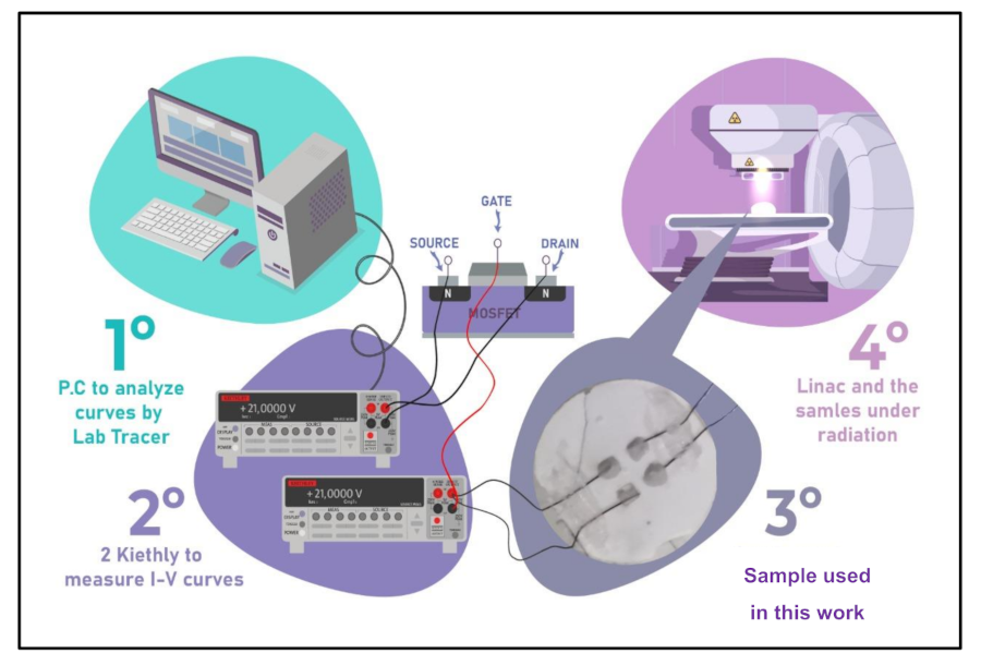
2. Materials and Methods
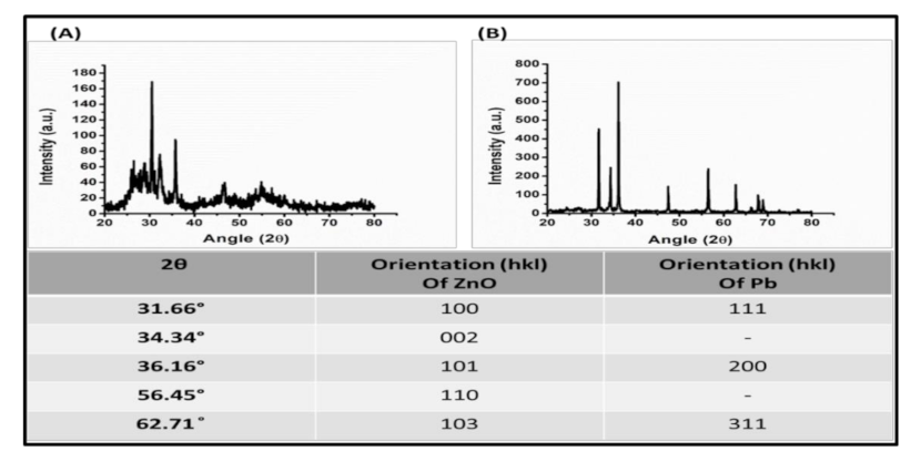
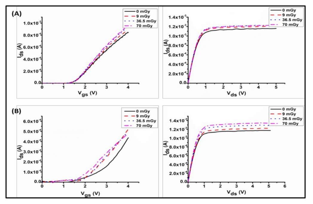
3. Results and Discussion
4. Conclusions
Author Contributions
Funding
Institutional Review Board Statement
Informed Consent Statement
Acknowledgments
Conflicts of Interest
References
- Arshak, K.; Korostynska, O. Response of metal oxide thin film structures to radiation. Mater. Sci. Eng. B 2006, 133, 1–7. [Google Scholar] [CrossRef]
- Thomson, I.; Thomas, R.; Berndt, L. Radiation dosimetry with MOS sensors. Radiat. Prot. Dosim. 1983, 6, 121–124. [Google Scholar] [CrossRef]
- Yin, L.-T.; Chou, J.-C.; Chung, W.-Y.; Sun, T.-P.; Hsiung, S.-K. Study of indium tin oxide thin film for separative extended gate ISFET. Mater. Chem. Phys. 2001, 70, 12–16. [Google Scholar] [CrossRef]
- Ahmed, N.M.; Kabaa, E.A.; Jaafar, M.S.; Omar, A.F. Characteristics of extended-gate field-effect transistor (EGFET) based on porous n-type (111) silicon for use in pH sensors. J. Electron. Mater. 2017, 46, 5804–5813. [Google Scholar] [CrossRef]
- Ristic, G.; Golubovic, S.; Pejovic, M. pMOS dosimeter with two-layer gate oxide operated at zero and negative bias. Electron. Lett. 1994, 30, 295–296. [Google Scholar] [CrossRef]
- Ristić, G.; Jakšić, A.; Pejović, M. pMOS dosimetric transistors with two-layer gate oxide. Sens. Actuators A Phys. 1997, 63, 129–134. [Google Scholar] [CrossRef]
- O’Connell, B.; Conneely, C.; McCarthy, C.; Doyle, J.; Lane, W.; Adams, L. Electrical performance and radiation sensitivity of stacked PMOS dosimeters under bulkbias control. IEEE Trans. Nucl. Sci. 1998, 45, 2689–2694. [Google Scholar] [CrossRef]
- Sarrabayrouse, G.; Buchdahl, D.; Polischuk, V.; Siskos, S. Stacked-MOS ionizing radiation dosimeters: Potentials and limitations. Radiat. Phys. Chem. 2004, 71, 737–739. [Google Scholar] [CrossRef]
- Sarrabayrouse, G.; Gessinn, F. Thick oxide MOS transistors for ionizing radiation dose measurement. Radioprotection 1994, 29, 557–572. [Google Scholar] [CrossRef] [Green Version]
- Vettese, F.; Donichak, C.; Bourgeault, P.; Sarrabayrouse, G. Assessment of a new p-MOSFET usable as a doserate insensitive gamma dose sensor. IEEE Trans. Nucl. Sci. 1996, 43, 991–996. [Google Scholar] [CrossRef]
- Pejovic, M.M. P-channel MOSFET as a sensor and dosimeter of ionizing radiation. Facta Univ. Ser. Electron. Energetics 2016, 29, 509–541. [Google Scholar] [CrossRef]
- Sze, S. Semiconductor device development in the 1970’s and 1980’s—A perspective. Proc. IEEE 1981, 69, 1121–1131. [Google Scholar] [CrossRef]
- Gordillo, G.; Calderon, C. Properties of ZnO thin films prepared by reactive evaporation. Sol. Energy Mater. Sol. Cells 2001, 69, 251–260. [Google Scholar] [CrossRef]
- Baydogan, N.; Ozdemir, O.; Cimenoglu, H. The improvement in the electrical properties of nanospherical ZnO: Al thin film exposed to irradiation using a Co-60 radioisotope. Radiat. Phys. Chem. 2013, 89, 20–27. [Google Scholar] [CrossRef]
- Özgür, Ü.; Alivov, Y.I.; Liu, C.; Teke, A.; Reshchikov, M.A.; Dogan, S.; Avrutin, V.; Cho, S.-J.; Morkoc, H. A comprehensive review of ZnO materials and devices. J. Appl. Phys. 2005, 98, 11. [Google Scholar] [CrossRef] [Green Version]
- Kannadasan, N.; Shanmugam, N.; Cholan, S.; Sathishkumar, K.; Viruthagiri, G.; Poonguzhali, R. Optical and electrochemical characteristics of Pb ions doped ZnO nanocrystals. Curr. Appl. Phys. 2014, 14, 1760–1766. [Google Scholar] [CrossRef]
- Kannadasan, N.; Shanmugam, N.; Sathishkumar, K.; Cholan, S.; Ponnguzhali, R.; Viruthagiri, G. Optical behavior and sensor activity of Pb ions incorporated ZnO nanocrystals. Spectrochim. Acta Part A Mol. Biomol. Spectrosc. 2015, 143, 179–186. [Google Scholar] [CrossRef] [PubMed]
- Ali, A.M.A.; Ahmed, N.M.; Kabir, N.A.; Almessiere, M.A. Multilayer ZnO/Pb/G thin film based extended gate field effect transistor for low dose gamma irradiation detection. Nucl. Instrum. Methods Phys. Res. Sect. A Accel. Spectrometers Detect. Assoc. Equip. 2021, 987, 164833. [Google Scholar] [CrossRef]
- Khan, F.M.; Gibbons, J.P. Khan’s the Physics of Radiation Therapy; Lippincott Williams & Wilkins: Philadelphia, PA, USA, 2014. [Google Scholar]
- Korostynska, O.; Hickey, G.; Forde, E. Ozone and gamma radiation sensing properties of In2O3: ZnO: SnO2 thin films. Microsyst. Technol. 2008, 14, 557–566. [Google Scholar] [CrossRef]
- Ali, A.M.A.; Ahmed, N.M.; Kabir, N.A.; Mohammad, S.M. Investigation on the characteristics of ZnO and ZnO-Pb structure for gamma radiation detection. J. Phys. Conf. Ser. 2020, 1535, 012028. [Google Scholar]
- Taherniya, A.; Raoufi, D. Thickness dependence of structural, optical and morphological properties of sol-gel derived TiO2 thin film. Mater. Res. Express 2018, 6, 016417. [Google Scholar] [CrossRef]
- Arshak, K.; Corcoran, J.; Korostynska, O. Gamma radiation sensing properties of TiO2, ZnO, CuO and CdO thick film pn-junctions. Sens. Actuators A Phys. 2005, 123, 194–198. [Google Scholar] [CrossRef]
- El-Mallawany, R.; Abousehly, A.; El-Rahamani, A.A.; Yousef, E. Radiation effect on the ultrasonic attenuation and internal friction of tellurite glasses. Mater. Chem. Phys. 1998, 52, 161–165. [Google Scholar] [CrossRef]
- Arshak, K.; Korostynska, O.; Harriss, J. /spl gamma/-radiation dosimetry using screen printed nickel oxide thick films. In Proceedings of the 23rd International Conference on Microelectronics, Nis, Yugoslavia, 12–15 May 2002; IEEE: Piscataway, NJ, USA, 2002. [Google Scholar]
- Pejović, M.; Ciraj-Bjelac, O.; Kovačević, M.; Rajović, Z.; Ilić, G. Sensitivity of P-channel MOSFET to X-and gamma-ray irradiation. Int. J. Photoenergy 2013, 2013, 158403. [Google Scholar] [CrossRef]
- Pejović, M.M.; Pejović, M.M.; Jakšić, A.B. Radiation-sensitive field effect transistor response to gamma-ray irradiation. Nucl. Technol. Radiat. Prot. 2011, 26, 25–31. [Google Scholar] [CrossRef]
- Asensio, L.; Carvajal, M.A.; Lopez-Villanueva, J.A.; Vilches, M.; Lallena, A.M.; Palma, A.J. Evaluation of a low-cost commercial mosfet as radiation dosimeter. Sens. Actuators A Phys. 2006, 125, 288–295. [Google Scholar] [CrossRef] [Green Version]
- Lavallée, M.C.; Gingras, L.; Beaulieu, L. Energy and integrated dose dependence of MOSFET dosimeter sensitivity for irradiation energies between and. Med. Phys. 2006, 33, 3683–3689. [Google Scholar] [CrossRef]
- Zhu, R.-Y. Radiation damage in scintillating crystals. Nucl. Instrum. Methods Phys. Res. Sect. A Accel. Spectrometers Detect. Assoc. Equip. 1998, 413, 297–311. [Google Scholar] [CrossRef] [Green Version]
- Pacchioni, G.; Pescarmona, P. Structure and stability of oxygen vacancies on sub-surface, terraces, and low-coordinated surface sites of MgO: An ab initio study. Surf. Sci. 1998, 412, 657–671. [Google Scholar] [CrossRef]
- Pacchioni, G. AB initio Theory of Point Defects in SiO2. In Defects in SiO2 and Related Dielectrics: Science and Technology; Springer: Berlin/Heidelberg, Germany, 2000; pp. 161–195. [Google Scholar]
- Holmes-Siedle, A.; Ravotti, F.; Glaser, M. The dosimetric performance of RADFETs in radiation test beams. In Proceedings of the 2007 IEEE Radiation Effects Data Workshop, Honolulu, HI, USA, 23–27 July 2007; IEEE: Piscataway, NJ, USA, 2007. [Google Scholar]
- Dozier, C.; Fleetwood, D.M.; Brown, D.B.; Winokur, P.S. An evaluation of low-energy X-ray and cobalt-60 irradiations of MOS transistors. IEEE Trans. Nucl. Sci. 1987, 34, 1535–1539. [Google Scholar] [CrossRef]


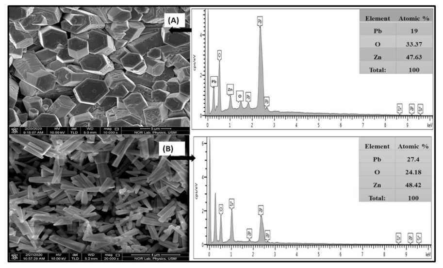
| Sample | TF Particle Size (nm) | Disk Particle Size (nm) | Effective Atomic Number |
|---|---|---|---|
| ZnO-Pb | 6.97 | 15.97 | 72.5 |
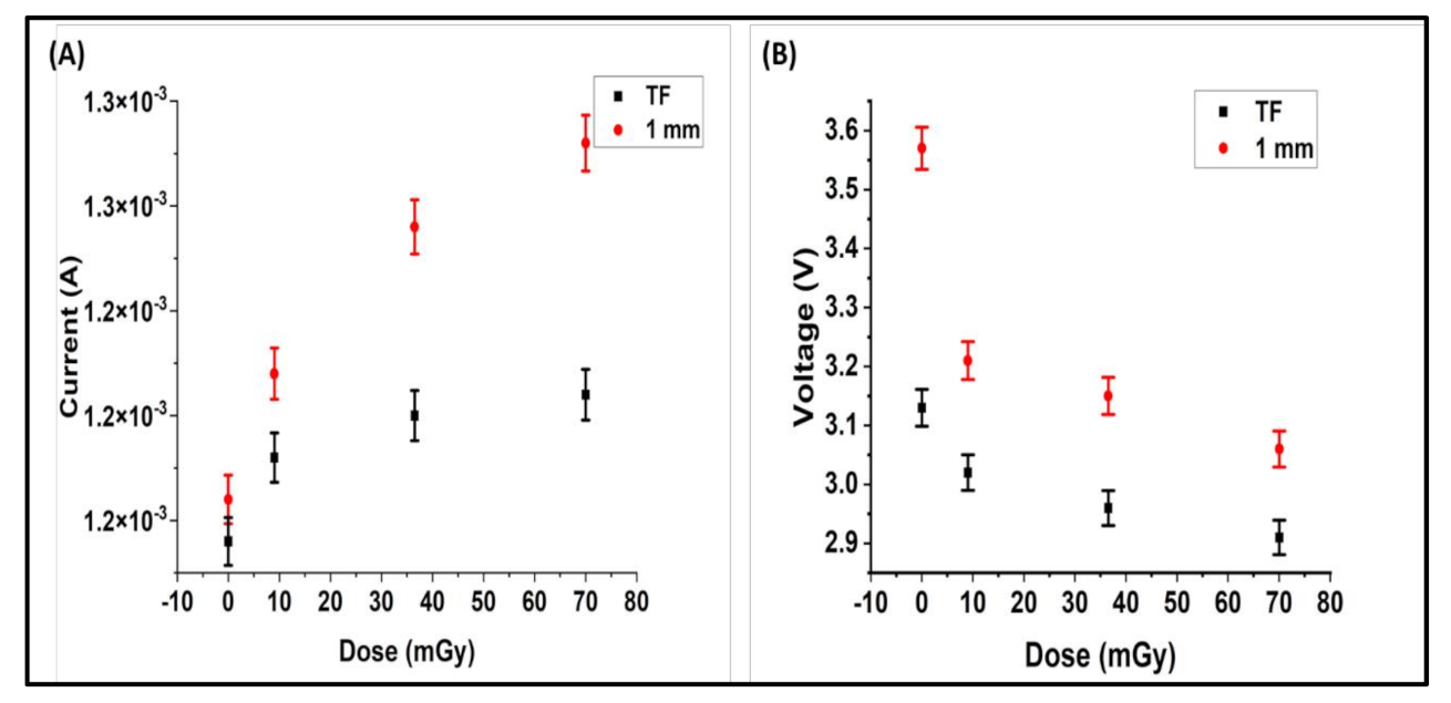
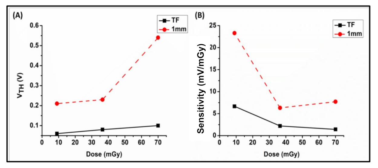
| Sample | Absorbed Dose (mGy) | Linearity % | Threshold Voltage (mV) | Sensitivity | |
|---|---|---|---|---|---|
| (mV/mGy) | (µA/mGy) | ||||
| TF ZnO-Pb | 9 | 94.5 | 60 | 6.66 | 1.05 |
| 36.5 | 80 | 2.19 | |||
| 70 | 100 | 1.42 | |||
| 1 mm disk ZnO-Pb | 9 | 96.5 | 210 | 23.3 | 2.28 |
| 36.5 | 230 | 6.30 | |||
| 70 | 540 | 7.71 | |||
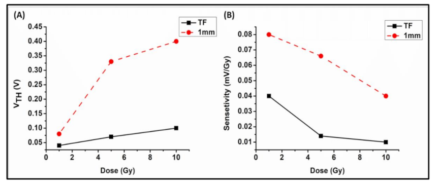
| Sample | Absorbed Dose (Gy) | Linearity (%) | Threshold Voltage (mV) | Sensitivity | |
|---|---|---|---|---|---|
| (mV/Gy) | (µA/Gy) | ||||
| TF ZnO-Pb | 1 | 90.4 | 0.04 | 0.04 | 5.80 |
| 5 | 0.07 | 0.014 | |||
| 10 | 0.1 | 0.01 | |||
| 1 mm disk ZnO-Pb | 1 | 96.8 | 0.08 | 0.08 | 21.5 |
| 5 | 0.33 | 0.066 | |||
| 10 | 0.4 | 0.04 | |||
Publisher’s Note: MDPI stays neutral with regard to jurisdictional claims in published maps and institutional affiliations. |
© 2021 by the authors. Licensee MDPI, Basel, Switzerland. This article is an open access article distributed under the terms and conditions of the Creative Commons Attribution (CC BY) license (https://creativecommons.org/licenses/by/4.0/).
Share and Cite
Ahmed Ali, A.M.; Ahmed, N.M.; Kabir, N.A.; Ali, M.K.M.; Akhdar, H.; Aldaghri, O.A.; Ibnaouf, K.H.; Sulieman, A. Investigation of X-ray Radiation Detectability Using Fabricated ZnO-PB Based Extended Gate Field-Effect Transistor as X-ray Dosimeters. Appl. Sci. 2021, 11, 11258. https://doi.org/10.3390/app112311258
Ahmed Ali AM, Ahmed NM, Kabir NA, Ali MKM, Akhdar H, Aldaghri OA, Ibnaouf KH, Sulieman A. Investigation of X-ray Radiation Detectability Using Fabricated ZnO-PB Based Extended Gate Field-Effect Transistor as X-ray Dosimeters. Applied Sciences. 2021; 11(23):11258. https://doi.org/10.3390/app112311258
Chicago/Turabian StyleAhmed Ali, Amal Mohamed, Naser M. Ahmed, Norlaili A. Kabir, Mohammed Khalil Mohammed Ali, Hanan Akhdar, Osamah A. Aldaghri, Khalid Hassan Ibnaouf, and Abdelmoneim Sulieman. 2021. "Investigation of X-ray Radiation Detectability Using Fabricated ZnO-PB Based Extended Gate Field-Effect Transistor as X-ray Dosimeters" Applied Sciences 11, no. 23: 11258. https://doi.org/10.3390/app112311258
APA StyleAhmed Ali, A. M., Ahmed, N. M., Kabir, N. A., Ali, M. K. M., Akhdar, H., Aldaghri, O. A., Ibnaouf, K. H., & Sulieman, A. (2021). Investigation of X-ray Radiation Detectability Using Fabricated ZnO-PB Based Extended Gate Field-Effect Transistor as X-ray Dosimeters. Applied Sciences, 11(23), 11258. https://doi.org/10.3390/app112311258