Article

Defect Processes in Halogen Doped SnO2

1
Institute of Nanoscience and Nanotechnology (INN), National Center for Scientific Research Demokritos, 15341 Agia Paraskevi, GR-11635 Athens, Greece
2
Faculty of Engineering, Environment and Computing, Coventry University, Priory Street, Coventry CV1 5FB, UK
3
Theoretical and Physical Chemistry Institute, National Hellenic Research Foundation, Vass. Constantinou 48, GR-11635 Athens, Greece
4
Department of Materials, Imperial College, London SW7 2AZ, UK
*
Author to whom correspondence should be addressed.
Appl. Sci. 2021, 11(2), 551; https://doi.org/10.3390/app11020551
Submission received: 11 December 2020 / Revised: 29 December 2020 / Accepted: 5 January 2021 / Published: 8 January 2021
(This article belongs to the Special Issue 10th Anniversary of Applied Sciences: Invited Papers in Materials)

Abstract

:
In the present study, we performed density functional theory calculations (DFT) to investigate structural changes and their impact on the electronic properties in halogen (F, Cl, Br, and I) doped tin oxide (SnO2). We performed calculations for atoms intercalated either at interstitial or substitutional positions and then calculated the electronic structure and the optical properties of the doped SnO2. In all cases, a reduction in the bandgap value was evident, while gap states were also formed. Furthermore, when we insert these dopants in interstitial and substitutional positions, they all constitute a single acceptor and donor, respectively. This can also be seen in the density of states through the formation of gap states just above the valence band or below the conduction band, respectively. These gap states may contribute to significant changes in the optical and electronic properties of SnO2, thus affecting the metal oxide’s suitability for photovoltaics and photocatalytic devices. In particular, we found that iodine (I) doping of SnO2 induces a high dielectric constant while also reducing the oxide’s bandgap, making it more efficient for light-harvesting applications.

1. Introduction

SnO2 is a wide bandgap, n-type semiconductor that adopts a tetragonal crystal structure [1,2,3,4,5,6]. Doping is also used to increase further its electrical conductivity as well as its transparency in the visible region [4,5,6]. SnO2 is mainly used as an opacifier of glazes [1], polishing powder [2], protective polymer coating [3], as a functional material in the solar cell technology [4], transparent conducting oxide [5,6] and gas sensor [7]. Recently Zhao et al. [8] demonstrated that a NO gas sensor based on Sn2O3 has an improved selectivity to NO, NO2, and CO gases [8]. Wang et al. [9] have shown that Sn3O4 in ultrathin SnO2 nanosheets exhibits great performance for Li-ion storage for battery technology. Furthermore, there are many experiments that examine the effect of halogen doping in SnO2 thin films with fluorine (F) being the most commonly used dopant because it significantly increases the conductivity and transparency of SnO2, hence making it appropriate for use as the transparent electrode in several classes of optoelectronics [10,11,12,13,14]. These include the sol-gel preparation of F:SnO2 nanostructures [11], studies on the structural characteristics, and the changes through the fluorine doping using X-ray diffraction (XRD) techniques [12] as well as deposition methods, such us spray pyrolysis [13] and chemical vapor deposition [14,15] for producing the F:SnO2. Regarding the F doping mechanism, several studies on F-doped SnO2 nanopowders using X-ray diffraction (XRD) analysis, transmission electron microscopy (TEM), X-ray photoelectron spectroscopy (XPS), and Fourier transformed infrared spectroscopy (FTIR) [16] revealed that at low concentration, F atoms occupy oxygen vacancy sites as substitutional dopants, but for higher concentrations F atoms site in interstitial positions in the host lattice. Moreover, few reports have also demonstrated the effects of chlorine (Cl), bromine (Br), and I doping in SnO2. Abass et al. [17,18,19], using several experiments with emphasis on optical and electrical properties, found pronounced improvements in these properties by halogen doping. Agashe et al. [20] also studied the electrical properties of sprayed deposited SnO2 films and showed that when replacing F dopants with Br, conductivity was reduced.
Except for experimental studies, there are also many theoretical research efforts using DFT that examine the role of defects such as F, Sb, and Cl in substitutional positions in SnO2 [21,22,23,24,25,26,27]. They revealed that such doping contributes to the formation of single donor states; however, the effect of interstitially doped SnO2 has not been studied yet. Additionally, the influence of other halogen dopants (besides F, Cl) in SnO2 and the corresponding changes in the oxide’s band structure and optical properties have not been systematically investigated yet. In most previously published DFT studies, the bandgap is significantly underestimated within the range 1 eV–2 eV [27,28,29]. This is a common problem when DFT calculations on wide bandgap semiconductors are conducted [30,31]. As a result, a number of methods have been developed in order to calculate more accurately the bandgap of these materials, with the Hubbard + U correction method and the computationally demanding but more accurate hybrid pseudopotentials being the most commonly used. Many researchers have applied the Hubbard + U method for the d orbitals of Sn, but still, the band gap was substantially underestimated (2.5 eV). In the case of hybrid pseudopotentials, although the band gap reaches the correct experimental value of 3.7 eV [32], the computational cost is very high, and this is why the majority of these researchers use a small number of atoms in their unit cells [33].
In the present study, we investigate the halogen doping of the bulk SnO2 using DFT in order to examine changes in the electronic structure as well as improvements in the photocatalytic properties of SnO2. To achieve such an endeavor, we apply hybrid DFT calculations. With this method, the bandgap reaches the correct value of 3.35 eV and it is in good agreement with similar DFT works [34]. We examined all the possible defect sites for the halogen dopants and we also calculated the minimum energies for these dopants being at interstitial positions and the changes in the electrical properties. Using the total density of states (DOS) and the projected density of states (pDOS), we analyzed the minimum energy sites of the defects and their effect on the bandgap. Furthermore, we predicted the optical properties of all the doping cases and we compared our results with the available experimental data.

2. Methodology

For the DFT calculations, we used the Cambridge Serial Total Energy Package (CASTEP) [35,36]. DFT calculations were performed using the Local Density Approximation (LDA) exchange-correlation Functional [37] with ultrasoft pseudopotentials [38]. The cutoff energy that met the convergence criteria was chosen at 800 eV and also for the geometry optimization of a 48 atom supercell, a 2 × 2 × 3 Monkhorst-Pack (MP) k-points set [39] was selected with the Broyden-Fletcher-Goldfard-Shanno (BFGS) method. As it was previously described, to consider the effects of the localized electrons, we used the hybrid functional PBE0 [39], which overcomes the LDA band gap error. Lastly, the DOS calculations were performed using a 3 × 3 × 3 k points mesh and the pDOS were performed using a k point mesh of 7 × 7 × 7. The convergence criteria for our analyses were chosen as 0.05 eV/Å for the Max force tolerance, 0.001 Å for the Max displacement tolerance, 0.1 GPa for the Max stress tolerance, and 2.0 × 10⁻⁵ eV/atom for the SCF tolerance.

3. Results

3.1. Structural Properties

SnO2 has a rutile structure and it belongs to the space group of P42/mmm (space group no 136) of the tetragonal system. The calculated lattice parameters of the unit cell are a = b = 4.717 Å and c = 3.189 Å (α = β = γ = 90°), in good agreement with the experimental results (a = b = 4.737 Å and c = 3.186 Å) [40]. In Figure 1a–h, the geometry of doped SnO2 structures is presented for the examined dopants (F, Cl, Br, and I) in substitutional and interstitial positions, where in each case the local distortion of the lattice is shown. The respective lattice parameters are presented in Table 1. An increase of cell dimensions due to the halogen incorporation in the SnO2 lattice is observed, as the substitution of oxygen with a larger atom (all halogens have a larger atomic radius than oxygen) will distort the lattice, increasing total volume, more so in the case of interstitial doping. It is interesting to note that in the case of iodine at an interstitial position, Ii, the cell increases in volume as both a and b increase, but the c parameter decreases. The anisotropic changes in the lattice parameters upon the introduction of the I atom is due to the reduction in the c-direction of the Sn-Ii bond length (3.31 Å) as compared to the Sn-I bond before our optimization (3.40 Å).

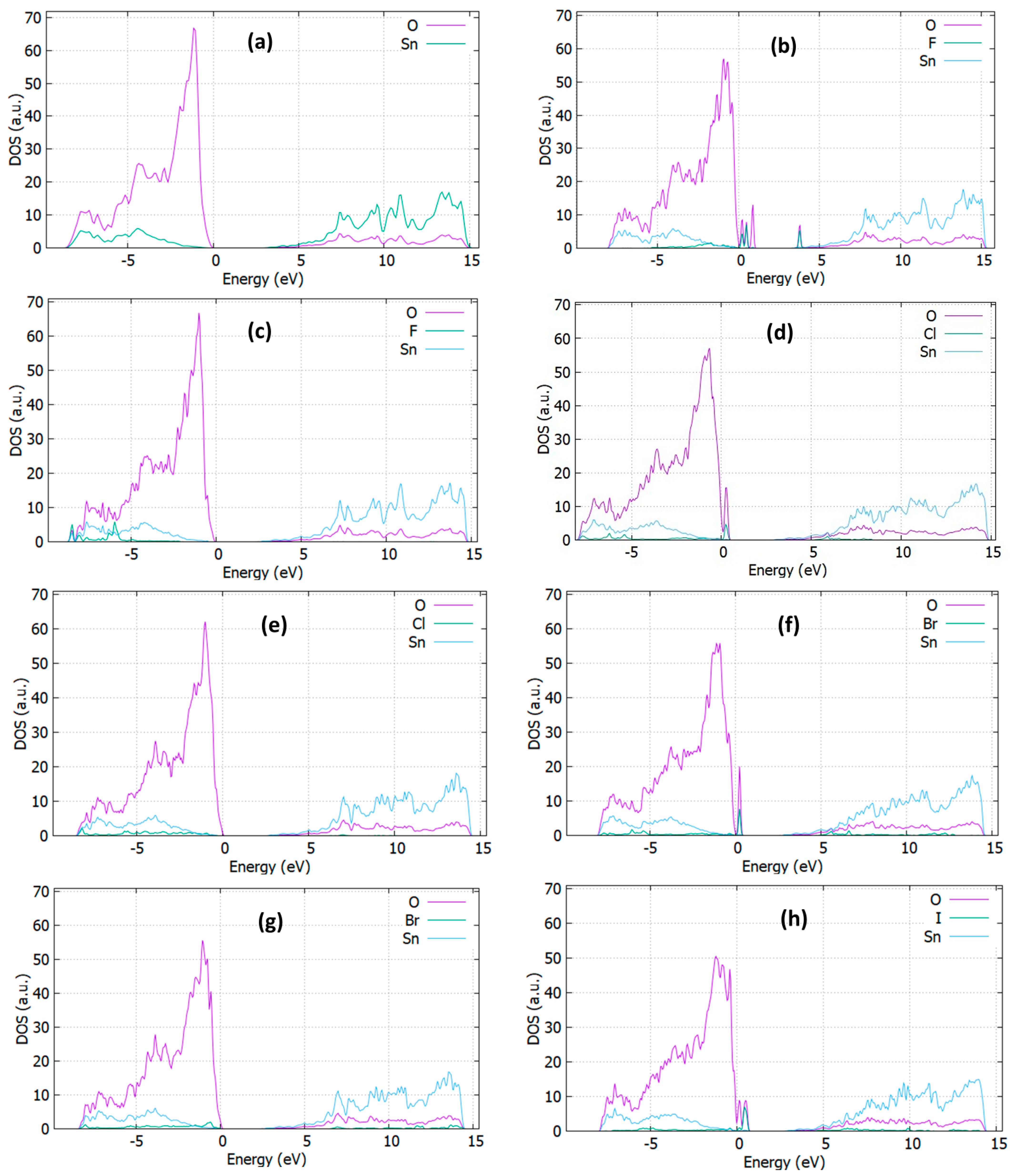
3.2. Electrical Properties

We examine the effect of halogen doping on the electronic properties and band gap of SnO2 by calculating the Density of States (DOS) of perfect and doped SnO2.
The bandgap of the undoped SnO2 is calculated using the PBE0 functional, at 3.35 eV (Figure 2a) close (but still underestimated) to the experimental value of 3.7 eV [32], in agreement with other theoretical studies [41,42,43]. As it is observed from Figure 2b, the F interstitial in SnO2 gives rise to energy states inside the band gap, near the band edges with a small reduction of 0.2 eV of the bandgap width, calculated at 3.12 eV (Figure 2b). When F is situated in an O-substitutional position, the bandgap is notably reduced to 2.90 eV without the presence of gap states (Figure 2c).
Regarding the Cl doping, in the case of interstitial doping, Cli: SnO2, the bandgap is further reduced to 2.85 eV with gap states present near the valence band. When Cl is at an O-substitutional position, Clo, a more significant bandgap reduction occurs, to 2.70 eV (Figure 2d,e). In a previous DFT research on F and Cl doped TiO2 [44], we also observed a significant bandgap reduction when a Cl atom was inserted in an interstitial position.
Regarding the effect of a Br interstitial intercalation (Figure 2f), the calculated bandgap is reduced to 2.90 eV with gap states near the valence band edge (minimum) are created. In comparison, in the case of substitutional Bro, the bandgap reaches a value of 2.71 eV (Figure 2g). It is evident that regarding the electronic structure, Br doping has the same effect as Cl doping in terms of bandgap reduction.
Lastly, I interstitial and substitutional doping is examined. We calculated that the bandgap is reduced to a value of 2.62 eV for the interstitial and 2.61 eV for the substitutional case, respectively, while states near the valence band are again presented. In this case, the substitutional doping has a smaller bandgap value than the interstitial case. This can be attributed to the states that are created to the valence band edge, which is due to the hybridization of the 2p orbitals of the nearest oxygen atom with the iodine 5p orbitals. As iodine is larger than the other halogens, even in the substitutional position, its orbitals are mixing with the nearest oxygen atom, giving rise to the states near the valence band. These results indicate that halogen interstitial dopants serve as single acceptors when they are intercalated within the SnO2 host lattice. Such gap states near the oxide’s valence band maximum and those near the conduction band position may act as shallow and deep acceptors, respectively, hence contributing to performance enhancements of devices based on doped SnO2. However, the gap states may also act as traps for the photogenerated carriers in specific photovoltaic devices such as organic and halide perovskite photovoltaics, thus decreasing the device photocurrent and overall performance.
However, the incorporation of substitutional halogen atoms in oxygen position does not introduce any gap states. This is in stark contrast with the intercalation of interstitial halogens that create some localized perturbations upon the upper valence band and the conduction band of the material. That implies free electrons’ presence contributing to the n-type conductivity, in accordance with experimental observations [45,46,47,48]. The halogen substitutional doping is seen to induce states inside or near the valence band. We believe that this can be explained because in the substitutional doping, the halogen orbitals are not mixing with the nearest Sn-5p or O-2p orbitals. As a result, no hybridized mid-gap states arise.
In Table 2 we have summarized our results. According to these calculations, the minimum value of the calculated bandgap is 2.61 eV for the case of Io doping. It is therefore suggested as the most effective of the halogen SnO2 dopants for photocatalytic applications.
Therefore, it is suggested that this type of doping can be used to develop better photocatalysts.
In Figure 3 and Figure 4, the pDOS for the doped SnO2 are shown. From the pDOS, we can gain important information about the gap states and the contribution of each element’s orbitals to the valence and conduction band. As seen in Figure 3a, which shows the pDOS of the plain SnO2, the valence band is mainly consisting of O-2p and Sn-5p orbitals, whereas the conduction band is created from the Sn-5s, Sn-5p, O-2s, and O-2p. This is in good agreement with previous theoretical studies [41,42]. Referring to Figure 3b, we see that F doped SnO2 has a similar valence and conduction band structure with the undoped SnO2 with a small deviation coming from the contribution of fluorine in the doped oxide. Focusing on the gap states formed near the valence band in the F-doped material, calculations show that it is created due to the hybridization of O-2p with F-2p orbitals (refer to Figure 4a). This is the same phenomenon that we predicted to occur in the case of TiO2 [43] upon doping with interstitial F atoms.
Similarly, in Figure 4b–d the rise of gap states is mainly created by the O-2p and Cl-2p and O-2p and Br-4p and I-5p. This probably indicates that the formation of mid-gap states in halogen doped n-type metal oxides such as SnO2 and TiO2 may have a universal origin. In any case, further investigation is needed, which is beyond the scope of the present manuscript.

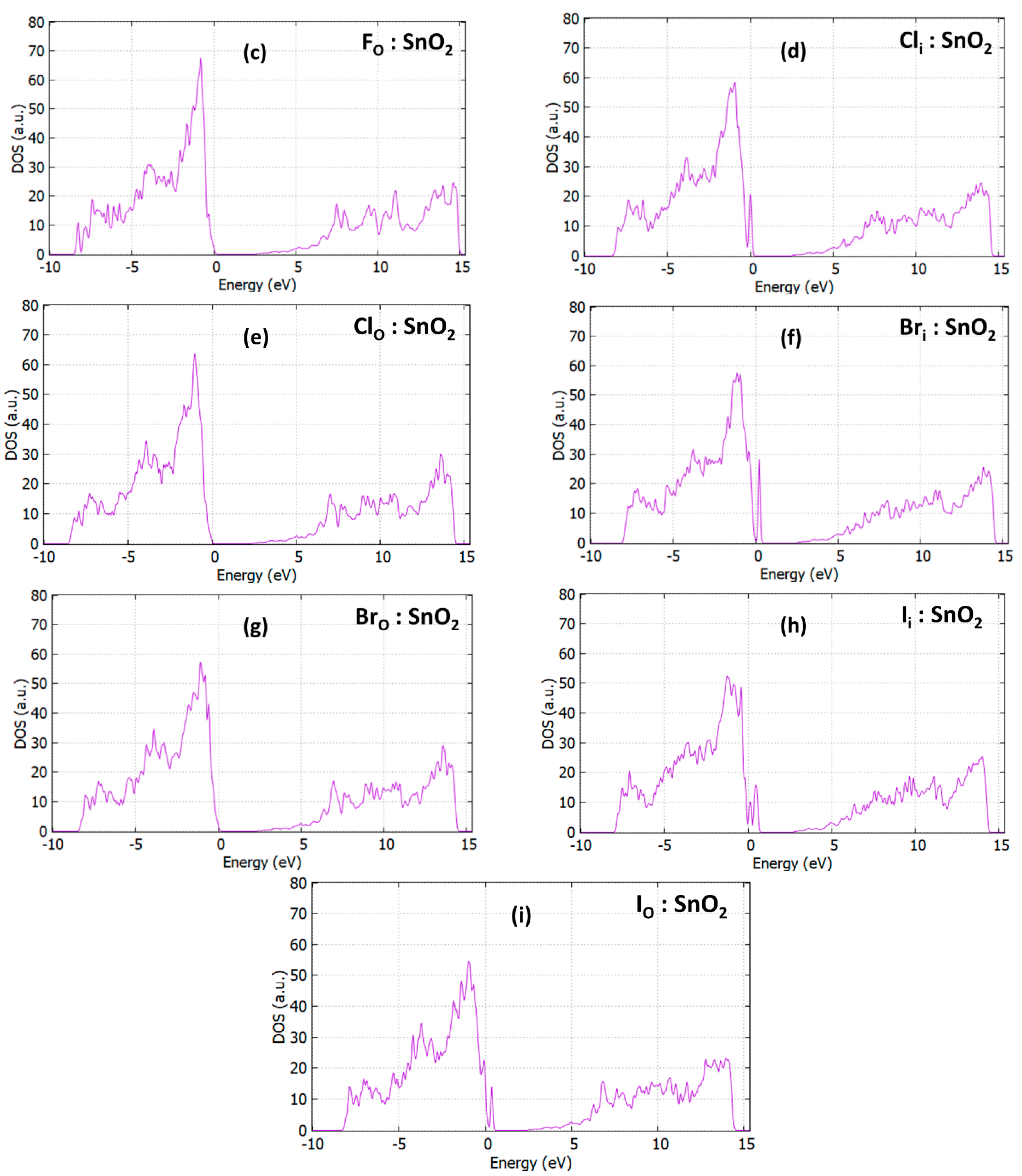
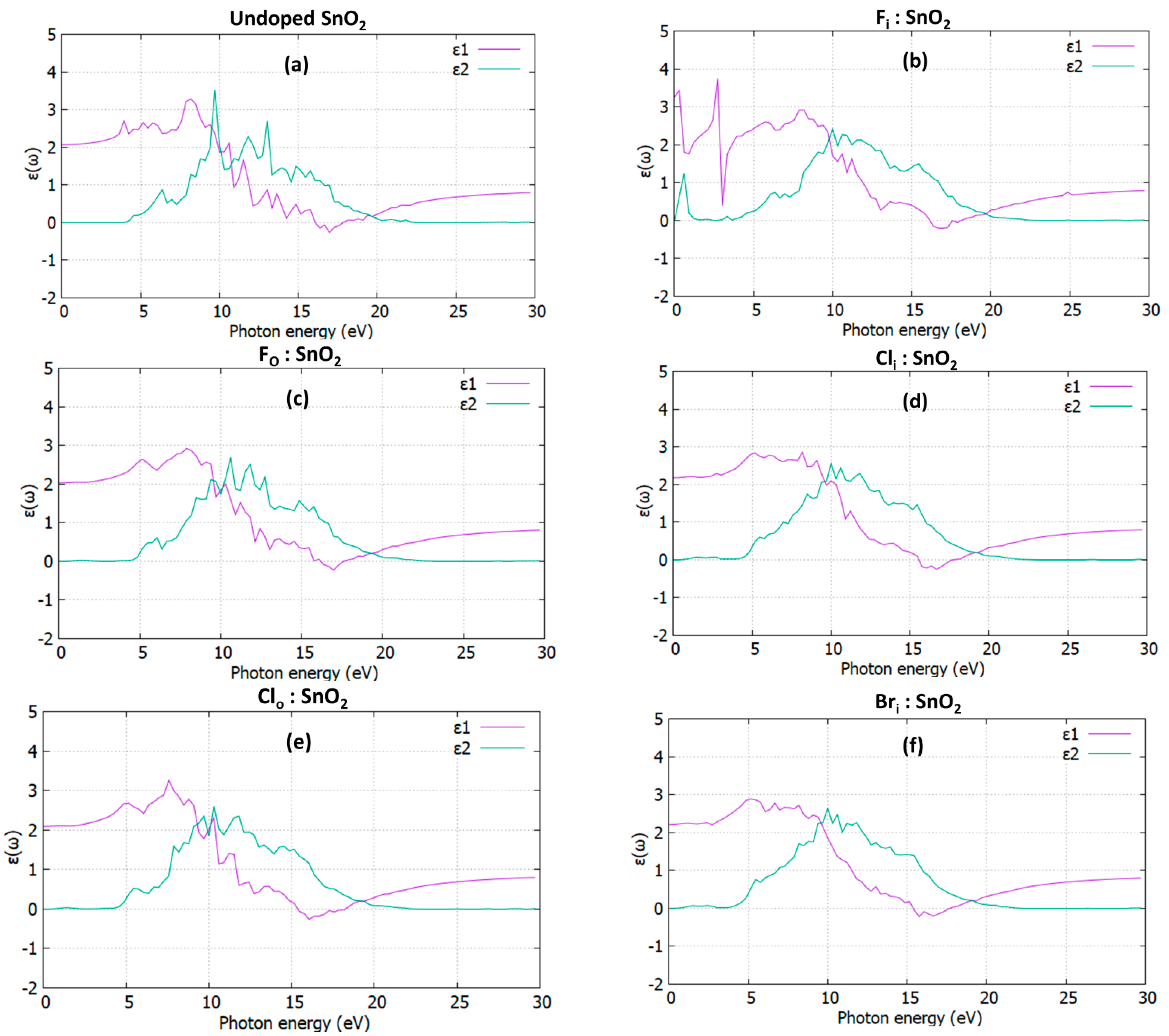
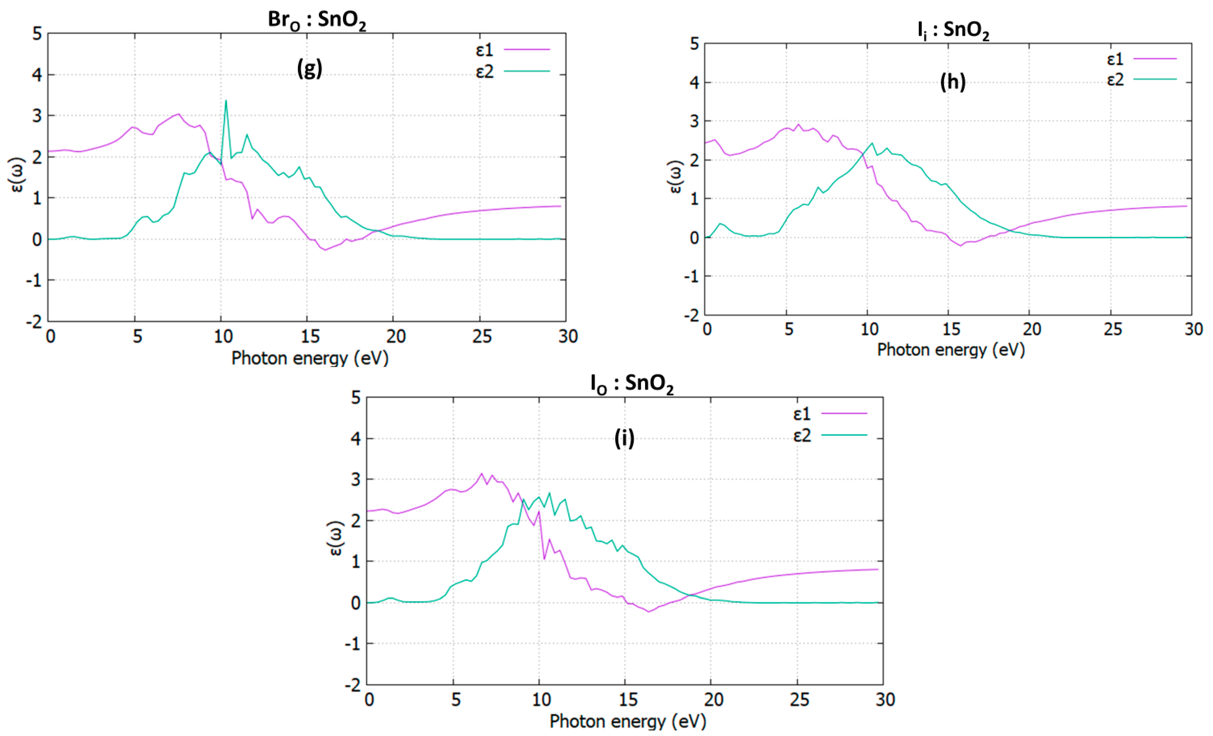
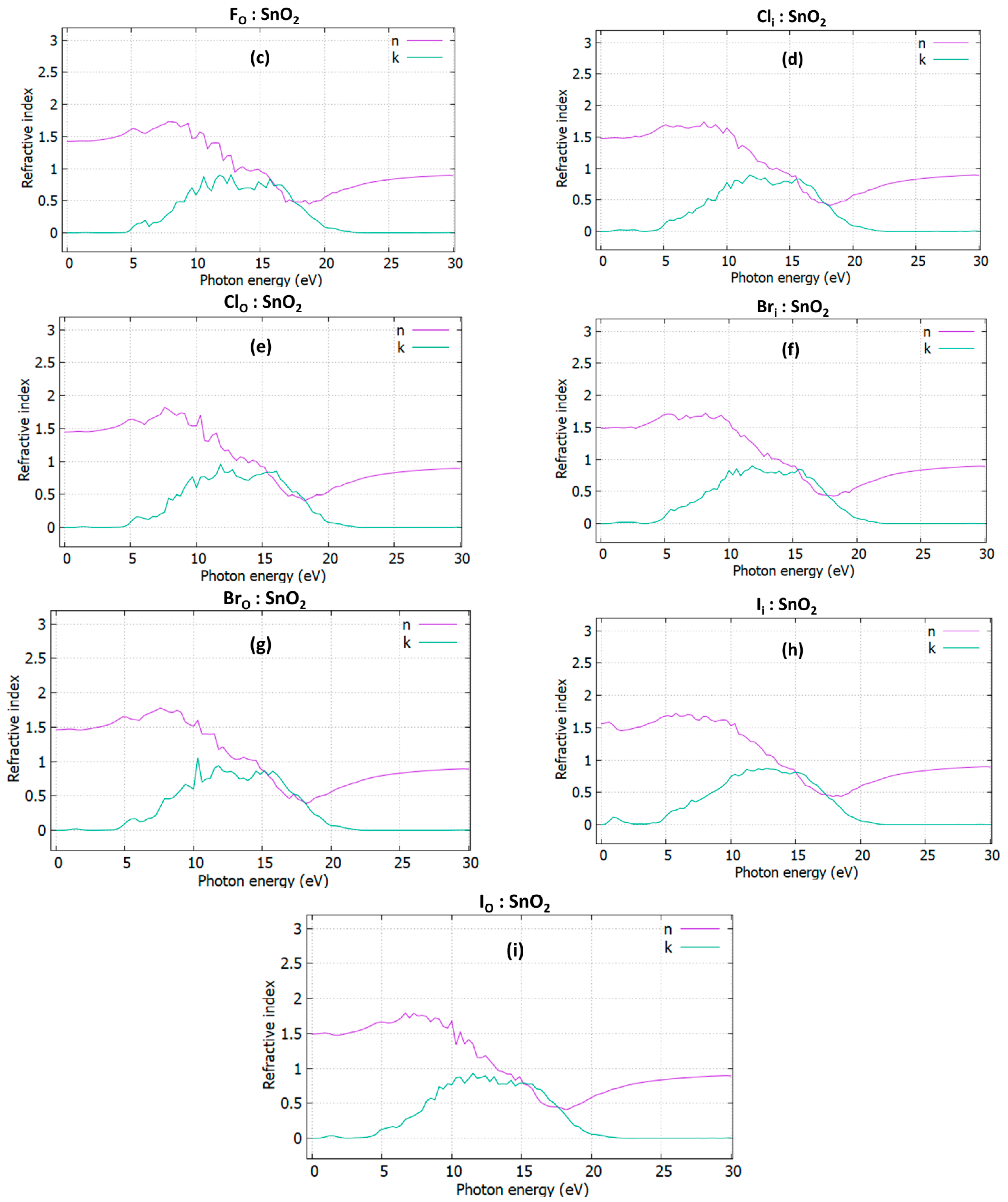
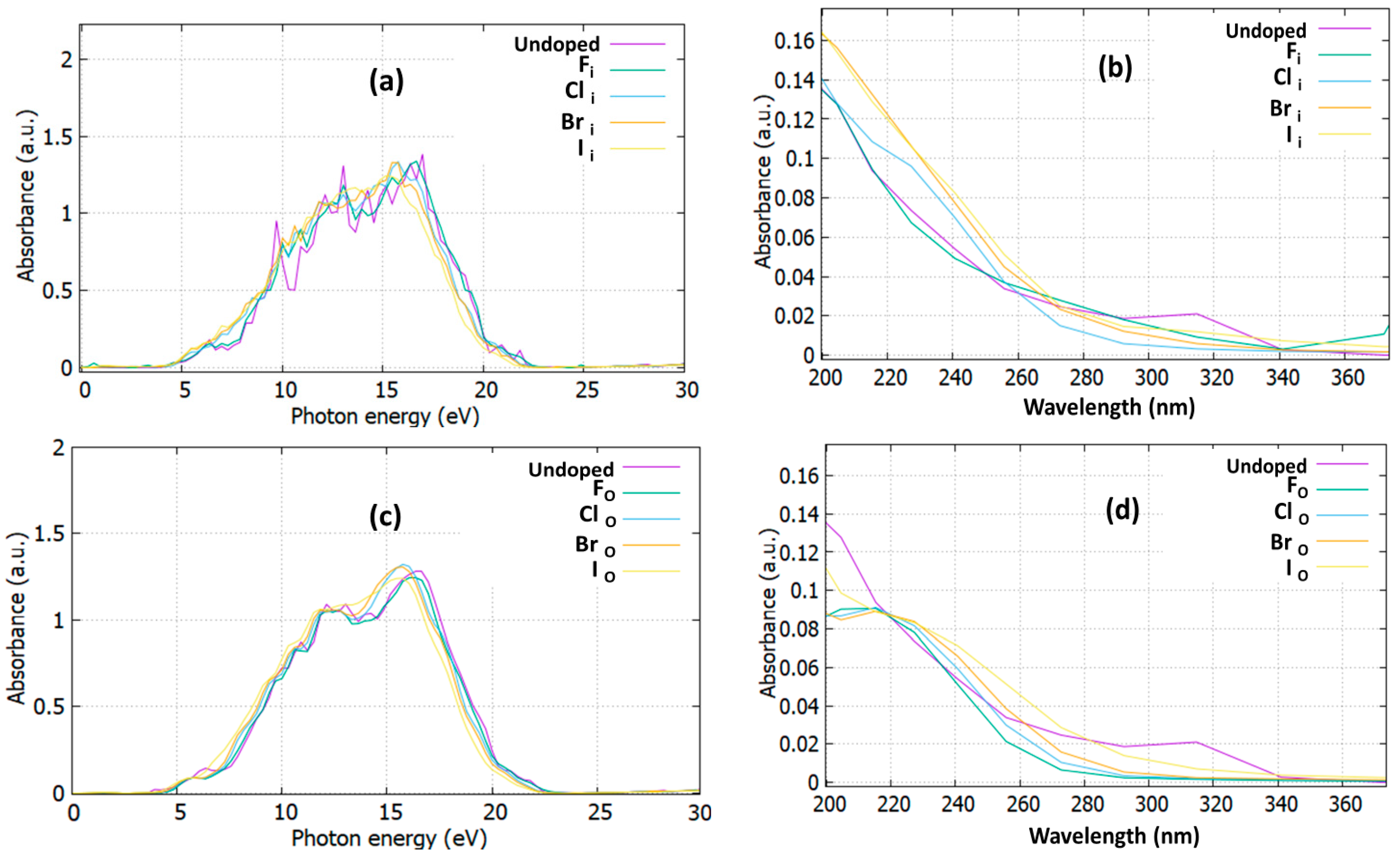
3.3. Optical Properties

The complex dielectric function can provide important information concerning the polarization mechanisms of the solid. The dominant dispersion/absorption mechanisms in the visible and ultraviolet range are caused by electronic excitations, i.e., transitions from occupied to empty electron levels. The dielectric function can describe these transitions.
In Figure 5a, the complex dielectric function of undoped SnO2 is presented. The real part of the dielectric function of the undoped SnO2 is descended as we increase the energy, reaching a maximum at 8.5 eV. The negative value in the energy range from 16–17 eV indicates that SnO2 has metallic properties [49,50]. The probability of photon absorption is calculated through the imaginary part of the dielectric function. Specifically, we observe two major peaks at 10 eV and at 12.5 eV, which are assigned to the electronic interband transition from O-2p to Sn 5p. The dielectric constant for the undoped case is calculated to 2, which agrees well with the experimental value of 1.6 [49] and similar DFT works predict a value of 2 [50]. In Figure 5b–i, all the dielectric functions for the doped cases are shown. It is evident that in the case of the interstitial doping with F, there is a notable improvement to the dielectric constant as it reaches the value of 3.2 from the real part of the dielectric function. The existence of a major peak at 1 eV can be attributed to the electronic transition of F-2p and the Sn-5p in the conduction band. As regards the other interstitial cases, it is predicted that the dielectric constant is almost unchanged except the Ii: SnO2, which shows an improvement, and it reaches a value of 2.7. For the substitutional doping cases, in the case of Io: SnO2, we calculate that the maximum value of the dielectric constant is achieved, which is 2.4.
The calculated refractive index (refer to Figure 6) for the undoped SnO2 is 1.40. This result is more underestimated than the experimental value of 1.70 [51], but agrees well with the value of other DFT studies [50]. The extinction coefficient can be described through the imaginary part of the refractive index, k. The major peak at the imaginary part of the undoped case is located at 12.5 eV. For the interstitial cases, we calculated that Fi shows an increase at the refractive index and reaches a value of 1.8. Afify et al. [52] experimentally predicted that the refractive index of F: SnO2 was between 1.85–2.2, which agrees well with the present study. For the substitutional cases, the refractive index has its maximum value of 1.51 in the case of Io: SnO2. The increase of the refractive index for Fi and Io boosts the antireflectivity (AR) of SnO2 and might be beneficial for application in energy harvesting devices.
Lastly, the absorption co-efficiency is presented in Figure 7. The major peaks range from 5 eV to 22 eV, and it is in good agreement with previous DFT studies [50]. The absorption of pure SnO2 starts at 380 nm, which is somewhat underestimated than the experimental value, which is around 400 nm [52]. It is seen that in the visible region (1.78–3.12 eV), I doped SnO2 has the highest absorption both for the interstitial and the substitutional positions.

4. Conclusions

DFT calculations were performed for halogen doped SnO2 and the effects of the exact kind of doping on the bandgap value and electronic properties were discussed. In this research, interstitial and substitutional halogen defects were examined. In all cases, it was observed that gap states were created from hybridization of O-2p with halogen 1s orbitals. Such energy states are beneficial for the oxide’s photocatalytic activity as they significantly reduce the optical band gap concerning that of undoped SnO2. They can also serve as charge transport paths in a certain type of optoelectronic device, whereas this might be detrimental for the application of halogen-doped oxide as electron transport material in other classes of photovoltaic devices. Iodine doped SnO2 has the lowest bandgap value of 2.60 eV and it is one of the lowest values reported for SnO2. Interestingly, when iodine resides in an oxygen site, it has a better refractive index and absorbance than the other halogen dopants. This makes it a suitable dopant candidate for SnO2-based energy harvesting devices.

Author Contributions

P.-P.F. and N.K. performed the DFT calculations, P.-P.F., N.K., M.V., A.C., wrote the paper, M.V., A.C. and D.D. contributed in the analysis and discussion of the results. All authors have read and agreed to the published version of the manuscript.

Funding

P.-P.F.: M.V., D.D. and A.C. are grateful for LRF ICON funding from the Lloyd’s Register Foundation charitable foundation helping to protect life and property by supporting engineering-related education, public engagement and the application of research. A.C. acknowledges support from European Union’s H2020 Programme under Grant Agreement no 824072- HARVESTORE.

Institutional Review Board Statement

Not applicable.

Informed Consent Statement

Not applicable.

Data Availability Statement

Not applicable.

Conflicts of Interest

The authors declare no conflict of interest.

References

  1. Searle, A.B. The Glazer’s Book; The Technical Press: London, UK, 1935. [Google Scholar]
  2. Holleman, A.F.; Wiberg, E. Inorganic Chemistry; Academic Press: Cambridge, MA, USA, 2001. [Google Scholar]
  3. Greenwood, N.N.; Earnshaw, A. Chemistry of the Elements; Elsevier: Amsterdam, The Netherlands, 2012. [Google Scholar]
  4. Tountas, M.; Topal, Y.; Kus, M.; Ersöz, M.; Fakis, M.; Argitis, P.; Vasilopoulou, M. Water-Soluble Lacunary Polyoxometalates with Excellent Electron Mobilities and Hole Blocking Capabilities for High Efficiency Fluorescent and Phosphorescent Organic Light Emitting Diodes. Adv. Funct. Mater. 2016, 26, 2655–2665. [Google Scholar] [CrossRef]
  5. Batzill, M.; Diebold, U. The Surface and Materials Science of Tin Oxide. Prog. Surf. Sci. 2005, 79, 47–154. [Google Scholar] [CrossRef]
  6. Fortunato, E.; Ginley, D.; Hosono, H.; Paine, D.C. Transparent conducting oxides for photovoltaics. MRS Bull. 2007, 32, 242–247. [Google Scholar] [CrossRef] [Green Version]
  7. Göpel, W.; Schierbaum, K.D. SnO2 sensors: Current status and future prospects. Sens. Actuators B Chem. 1995, 26, 1–12. [Google Scholar] [CrossRef]
  8. Zhao, J.; Tan, R.; Shen, W.; Yang, Y.; Guo, Y.; Li, J.; Zhou, Z.; Jian, J.; Song, W. Highly selective Sn2O3-based sensors for NO detection. Mater. Lett. 2012, 84, 94–96. [Google Scholar] [CrossRef]
  9. Wang, C.; Du, G.; Ståhl, K.; Huang, H.; Zhong, Y.; Jiang, J.Z. Ultrathin SnO2 nanosheets: Oriented attachment mechanism, nonstoichiometric defects, and enhanced lithium-ion battery performances. J. Phys. Chem. C 2012, 116, 4000–4011. [Google Scholar] [CrossRef] [Green Version]
  10. Rakhshani, A.E.; Makdisi, Y.; Ramazaniyan, H.A. Electronic and optical properties of fluorine-doped tin oxide films. J. Appl. Phys. 1998, 83, 1049–1057. [Google Scholar] [CrossRef]
  11. Wu, S.; Yuan, S.; Shi, L.; Zhao, Y.; Fang, J. Preparation, characterization and electrical properties of fluorine-doped tin dioxide nanocrystals. J. Coll. Interface Sci. 2010, 346, 12–16. [Google Scholar] [CrossRef]
  12. Garces, F.A.; Budini, N.; Koropecki, R.R.; Arce, R.D. Structural mosaicity and electrical properties of pyrolytic SnO2:F thin films. Thin Solid Films 2013, 531, 172–178. [Google Scholar] [CrossRef]
  13. Elangovan, E.; Ramamurthi, K. A study on low cost-high conducting fluorine and antimony-doped tin oxide thin films. Appl. Surf. Sci. 2005, 249, 183–196. [Google Scholar] [CrossRef]
  14. Yang, J.; Liu, W.; Dong, L.; Li, Y.; Li, C.; Zhao, H. Studies on the structural and electrical properties of F-doped SnO2 film prepared by APCVD. Appl. Surf. Sci. 2011, 257, 10499–10502. [Google Scholar] [CrossRef]
  15. Moholkar, A.V.; Pawar, S.M.; Rajpure, K.Y.; Bhosale, C.H.; Kim, J.H. Effect of fluorine doping onhighly transparent conductive spray deposited nanocrystalline tin oxide thin flms. Appl. Surf. Sci. 2009, 255, 9358–9364. [Google Scholar] [CrossRef]
  16. Suffner, J.; Ágoston, P.; Kling, J.; Hahn, H. Chemical vapor synthesis of fluorine-doped SnO2 (FTO) nanoparticles. J. Nanopart. Res. 2010, 12, 2579–2588. [Google Scholar] [CrossRef]
  17. Abass, A.K. Electrical and optical properties of chlorine doped SnO2 coatings. Solid State Commun. 1987, 61, 507–510. [Google Scholar] [CrossRef]
  18. Abass, A.K.; Bakr, H.; Jassim, S.A.; Fahad, T.A. Electrical and optical properties of chemically deposited SnO2: I coatings. Sol. Energy Mater. 1988, 17, 425–431. [Google Scholar] [CrossRef]
  19. Abass, A.K.; Al-Liabi, N.A.; Taha, W.A. Optical properties of bromine-doped SnO2 coatings for solar applications. Phys. Status Solidi (a) 1988, 106, 613–618. [Google Scholar] [CrossRef]
  20. Agashe, C.; Major, S.S. Effect of F, Cl and Br doping on electrical properties of sprayed SnO2 films. J. Mater. Sci. Lett. 1996, 15, 497–499. [Google Scholar] [CrossRef]
  21. Peng-Fei, L.; Yue, S.; Zhong-Yuan, Y.; Long, Z.; Qiong-Yao, L.; Shi-Jia, L.M.; Li-Hong, H.; Yu-Min, L. Electronic structure and optical properties of antimony-doped SnO2 from first-principle study. Commun. Theor. Phys. 2012, 57, 145. [Google Scholar]
  22. Canestraro, C.D.; Roman, L.S.; Persson, C. Polarization dependence of the optical response in SnO2 and the effects from heavily F doping. Thin Solid Films 2009, 517, 6301–6304. [Google Scholar] [CrossRef]
  23. Rivera, R.; Marcillo, F.; Chamba, W.; Puchaicela, P.; Stashans, A. SnO2 physical and chemical properties due to the impurity doping. Lect. Notes Eng. Comp. 2013, 2, 814–818. [Google Scholar]
  24. Velikokhatnyi, O.I.; Kumta, P.N. Ab-initio study of fluorine-doped tin dioxide: A prospective catalyst support for water electrolysis. Physica B 2011, 406, 471–477. [Google Scholar] [CrossRef]
  25. Golovanov, V.; Golovanova, V.; Kuisma, M.; Rantala, T.T. Electron spin resonance parameters of cation vacancies in tin dioxide doped with fluorine and hydrogen. J. Appl. Phys. 2013, 114, 143907. [Google Scholar] [CrossRef]
  26. Oshima, M.; Yoshino, K. Structural and Electronic Structure of SnO2 by the First-Principle Study. Mater. Sci. Forum 2012, 725, 265–268. [Google Scholar] [CrossRef]
  27. Govaerts, K.; Partoens, B.; Lamoen, D. Extended homologous series of Sn–O layered systems: A first-principles study. Solid State Comm. 2016, 243, 36–43. [Google Scholar] [CrossRef] [Green Version]
  28. Marcillo, F.; Stashans, A. DFT calculations of tin dioxide crystals containing heavily-doped fluorine. J. Theor. Comput. Chem. 2014, 13, 1450069. [Google Scholar] [CrossRef]
  29. Perdew, J.P.; Levy, M. Physical content of the exact Kohn-Sham orbital energies: Band gaps and derivative discontinuities. Phys. Rev. Lett. 1983, 51, 1884. [Google Scholar] [CrossRef]
  30. Sham, L.J.; Schlüter, M. Density-functional theory of the energy gap. Phys. Rev. Lett. 1983, 51, 1888. [Google Scholar] [CrossRef]
  31. Thangaraju, B. Structural and electrical studies on highly conducting spray deposited fluorine and antimony doped SnO2 thin films from SnCl2 precursor. Thin Solid Films 2002, 402, 71–78. [Google Scholar] [CrossRef] [Green Version]
  32. Zervos, M.; Lathiotakis, N.; Kelaidis, N.; Othonos, A.; Tanasa, E.; Vasile, E. Epitaxial Highly Ordered Sb:SnO2 Nanowires Grown by the Vapor Liquid Solid Mechanism on m-, r- and a-Al2O3. Nanoscale Adv. 2019, 1, 1980–1990. [Google Scholar] [CrossRef] [Green Version]
  33. Deng, H.X.; Li, S.S.; Li, J. Quantum confinement effects and electronic properties of SnO2 quantum wires and dots. J. Phys. Chem. C 2010, 114, 4841–4845. [Google Scholar] [CrossRef]
  34. Payne, M.C.; Teter, M.P.; Allan, D.C.; Arias, T.A.; Joannopoulos, J.D. CASTEP 4.2 Academic version, licensed under the UKCP-MSI Agreement. Rev. Mod. Phys. 1992, 64, 1045–1097. [Google Scholar] [CrossRef] [Green Version]
  35. Segall, M.D.; Lindan, P.J.; Probert, M.A.; Pickard, C.J.; Hasnip, P.J.; Clark, S.J.; Payne, M.C. First-principles simulation: Ideas, illustrations and the CASTEP code. J. Phys. Cond. Matter 2002, 14, 2717–2744. [Google Scholar] [CrossRef]
  36. Ceperley, D.M.; Alder, B.J. Exchange-correlation potential and energy for density-functional calculation. Phys. Rev. Lett. 1980, 45, 567–581. [Google Scholar]
  37. Vanderbilt, D. Soft self-consistent pseudopotentials in a generalized eigenvalue formalism. Phys. Rev. B 1990, 41, 7892–7895. [Google Scholar] [CrossRef]
  38. Monkhorst, H.J.; Pack, J.D. Special points for Brillouin-zone integrations. Phys. Rev. B 1976, 13, 5188–5192. [Google Scholar] [CrossRef]
  39. Paier, J.; Marsman, M.; Hummer, K.; Kresse, G.; Gerber, I.C.; Angyan, J.G. Screened hybrid density functionals applied to solids. J. Chem. Phys. 2006, 124, 154709. [Google Scholar] [CrossRef] [PubMed] [Green Version]
  40. Xu, J.; Huang, S.; Wang, Z. First principle study on the electronic structure of fluorine-doped SnO2. Solid State Commun. 2009, 149, 527–531. [Google Scholar] [CrossRef]
  41. Yahla, H.; Boukra, A.; Belhakem, M.; Lippens, P.E. First-principles calculations of the electronic structure and Mössbauer parameters of Sb-doped SnO2. Solid State Commun. 2009, 149, 2202–2206. [Google Scholar] [CrossRef]
  42. Borges, P.D.; Scolfaro, L.M.; Alves, H.W.L.; da Silva, E.F. DFT study of the electronic, vibrational, and optical properties of SnO2. Theor. Chem. Acc. 2009, 126, 39–44. [Google Scholar] [CrossRef]
  43. Filippatos, P.P.; Kelaidis, N.; Vasilopoulou, M.; Davazoglou, D.; Lathiotakis, N.N.; Chroneos, A. Defect processes in F and Cl doped anatase TiO2. Sci. Rep. 2019, 9, 19970. [Google Scholar] [CrossRef] [PubMed]
  44. Ramaiah, K.S.; Raja, V.S. Structural and electrical properties of fluorine doped tin oxide films prepared by spray-pyrolysis technique. Appl. Surf. Sci. 2006, 253, 1451–1458. [Google Scholar] [CrossRef]
  45. Yadav, A.A.; Masumdar, E.U.; Moholkar, A.V.; Neumann-Spallart, M.; Rajpure, K.Y.; Bhosale, C.H. Electrical, structural and optical properties of SnO2:F thin films: Effect of the substrate temperature. J. Alloys Compd. 2009, 488, 350–355. [Google Scholar] [CrossRef]
  46. Elangovan, E.; Ramamurthi, K. Studies on micro-structural and electrical properties of spray-deposited fluorine-doped tin oxide thin films from low-cost precursor. Thin Solid Films 2005, 476, 231–236. [Google Scholar] [CrossRef]
  47. Chinnappa, L.; Ravichandran, K.; Saravanakumar, K.; Muruganantham, G.; Sakthivel, B. The combined effects of molar concentration of the precursor solution and fluorine doping on the structural and electrical properties of tin oxide films. J. Mater. Sci. Mater. Electron. 2001, 22, 1827–1834. [Google Scholar] [CrossRef]
  48. Bakr, N.A.; Salman, S.A.; Ali, M.N. Effect of Fluorine Doping on Structural and Optical Properties of SnO2 Thin Films Prepared by Chemical Spray Pyrolysis Method. Adv. Mater. 2006, 5, 23. [Google Scholar] [CrossRef] [Green Version]
  49. Tingting, S.; Fuchun, Z.; Weihu, Z. Density functional theory study on the electronic structure and optical properties of SnO2. Rare Met. Mat. Eng. 2015, 44, 2409–2414. [Google Scholar] [CrossRef]
  50. Khan, A.F.; Mehmood, M.; Aslam, M.; Ashraf, M. Characteristics of electron beam evaporated nanocrystalline SnO2 thin films annealed in air. Appl. Surf. Sci. 2010, 256, 2252–2258. [Google Scholar] [CrossRef]
  51. Afify, H.H.; Momtaz, R.S.; Badawy, W.A.; Nasser, S.A. Some physical properties of fluorine-doped SnO2 films prepared by spray pyrolysis. J. Mater. Sci. Mater. Electron. 1991, 2, 40–45. [Google Scholar] [CrossRef]
  52. Doyan, A.; Susilawati; Imawanti, Y.D. Synthesis and Characterization of SnO2 thin layer with a doping Aluminum is deposited on Quartz Substrates. AIP Conf. Proc. 2017, 1801, 020005. [Google Scholar]
Figure 1. (a) Fo: SnO2, (b) Fi: SnO2, (c) Clo: SnO2, (d) Cli: SnO2, (e) Bro: SnO2, (f) Bri: SnO2, (g) Io: SnO2, (h) Ii: SnO2.
Applsci 11 00551 g001aApplsci 11 00551 g001b
Figure 2. The Density of States (DOS) of the (a) undoped SnO2, (b) Fi doped SnO2, (c) Fo doped SnO2, (d) Cli doped SnO2, (e) Clo doped SnO2, (f) Bri doped SnO2, (g) BrO doped SnO2, (h) Ii doped SnO2, and (i) IO doped SnO2.
Applsci 11 00551 g002aApplsci 11 00551 g002b
Figure 3. pDOS graphs of (a) undoped SnO2, (b) Fi doped SnO2, (c) Fo doped SnO2, (d) Cli doped SnO2, (e) Clo doped SnO2, (f) Bri doped SnO2, (g) BrO doped SnO2, (h) Ii doped SnO2, and (i) IO doped SnO2.
Applsci 11 00551 g003aApplsci 11 00551 g003b
Figure 4. (a) The gap states of the Fi doped SnO2; (b) The gap states of the Cli doped SnO2; (c) The gap states of Bri doped SnO2; (d) The gap states of Ii doped SnO2.
Applsci 11 00551 g004
Figure 5. The dielectric function of the (a) undoped SnO2, (b) Fi doped SnO2, (c) Fo doped SnO2, (d) Cli doped SnO2, (e) Clo doped SnO2, (f) Bri doped SnO2, (g) BrO doped SnO2, (h) Ii doped SnO2, and (i) IO doped SnO2.
Applsci 11 00551 g005aApplsci 11 00551 g005b
Figure 6. The refractive index of the (a) plain SnO2, (b) Fi doped SnO2, (c) Fo doped SnO2, (d) Cli doped SnO2, (e) Clo doped SnO2, (f) Bri doped SnO2, (g) BrO doped SnO2, (h) Ii doped SnO2, and (i) IO doped SnO2.
Applsci 11 00551 g006aApplsci 11 00551 g006b
Figure 7. The absorption for (a) interstitially doped SnO2 for all the energy spectrum, (b) interstitially doped SnO2 as a function of the wavelength, (c) substitutionally doped SnO2 for all the energy spectrum, (d) substitutionally doped SnO2 as a function of the wavelength.
Applsci 11 00551 g007
Table 1. The computed lattice parameters and cell volumes for every doping case.
a (Å)b (Å)c (Å)Vol (Å3)
SnO24.7174.7173.18970.956
Fi: SnO24.7394.7153.19571.390
Fo: SnO24.7354.7353.20571.857
Cli: SnO24.7894.7903.20173.429
CloSnO24.7784.7783.21373.350
Bri: SnO24.7954.8453.19474.202
Bro: SnO24.7954.7953.21873.988
Ii: SnO25.0554.8303.16577.276
Io: SnO24.8404.8403.21575.313
Table 2. Band gap values for every halogen doping case.
Halogen DopantsBand Gap
Interstitial DopingSubstitutional Doping
F3.122.90
Cl2.852.70
Br2.902.71
I2.622.61
Publisher’s Note: MDPI stays neutral with regard to jurisdictional claims in published maps and institutional affiliations.

