
Power Sharing Control in a Grid-Tied DC Microgrid: Controller Hardware in the Loop Validation

 ,
,  and
and 
Abstract
:1. Introduction
2. MGIS: Description, Modeling, and Design
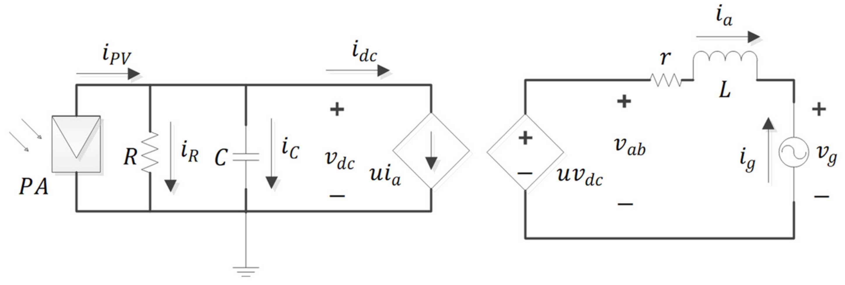
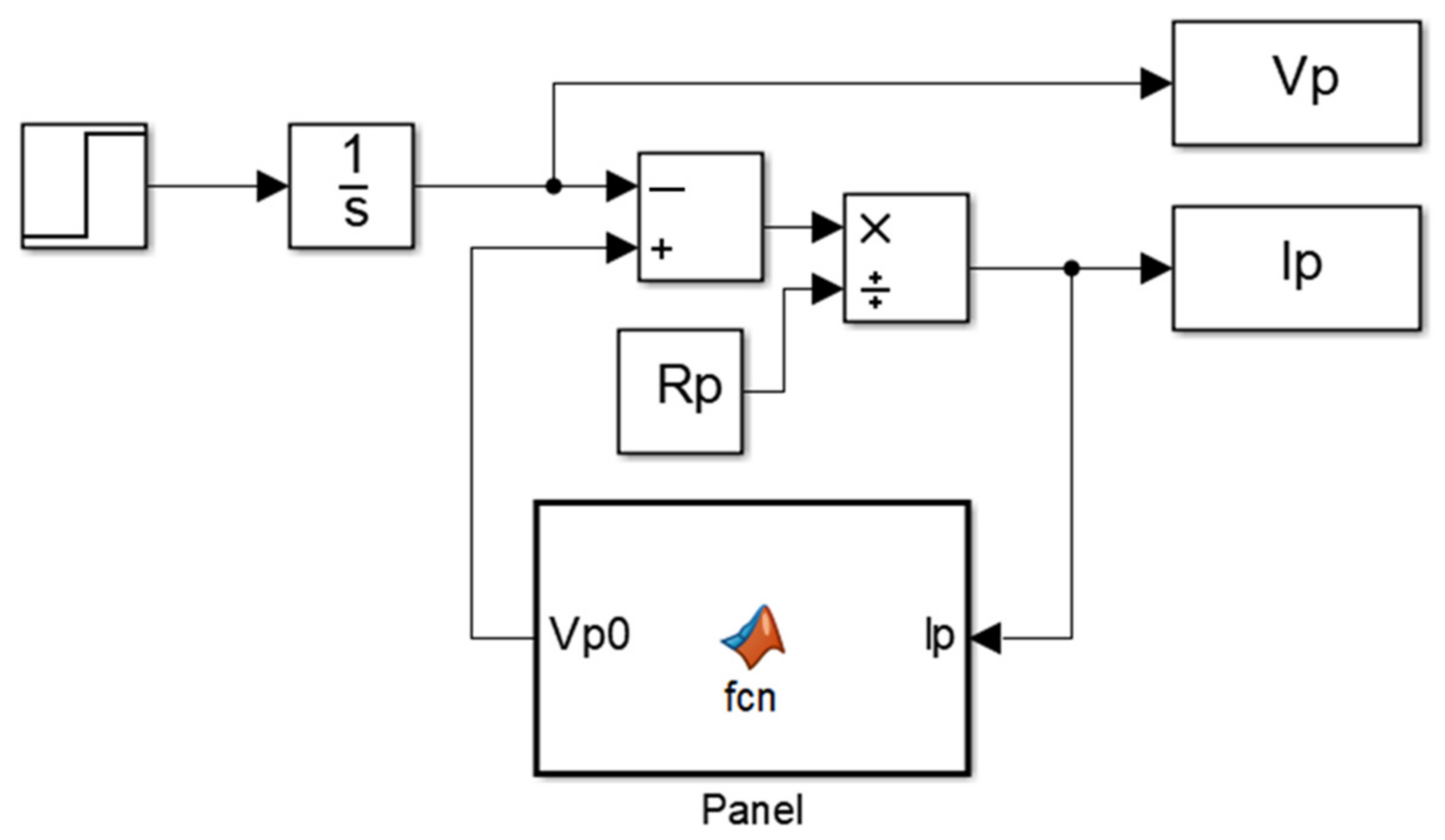
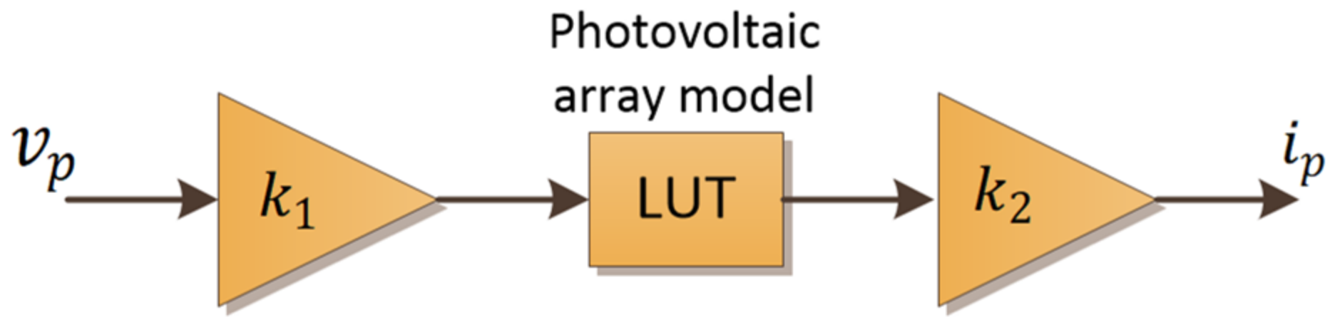
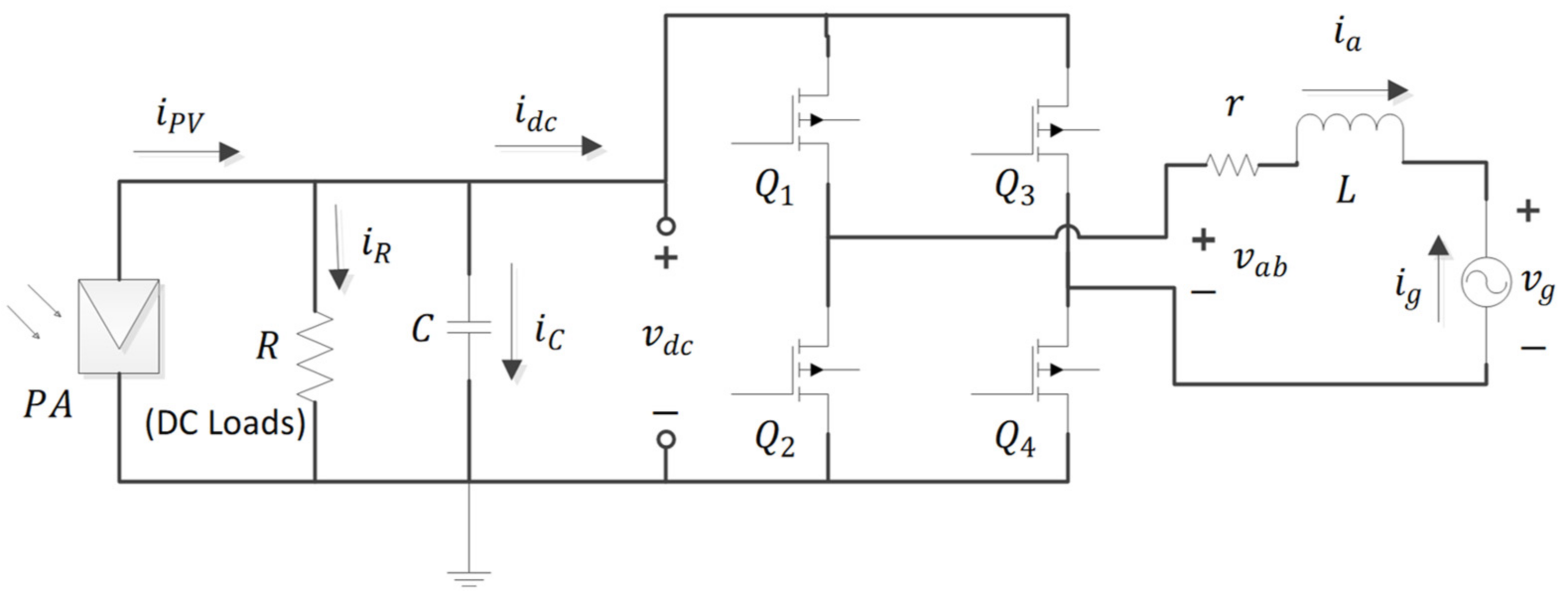
2.1. Photovoltaic Array Description and Modelling
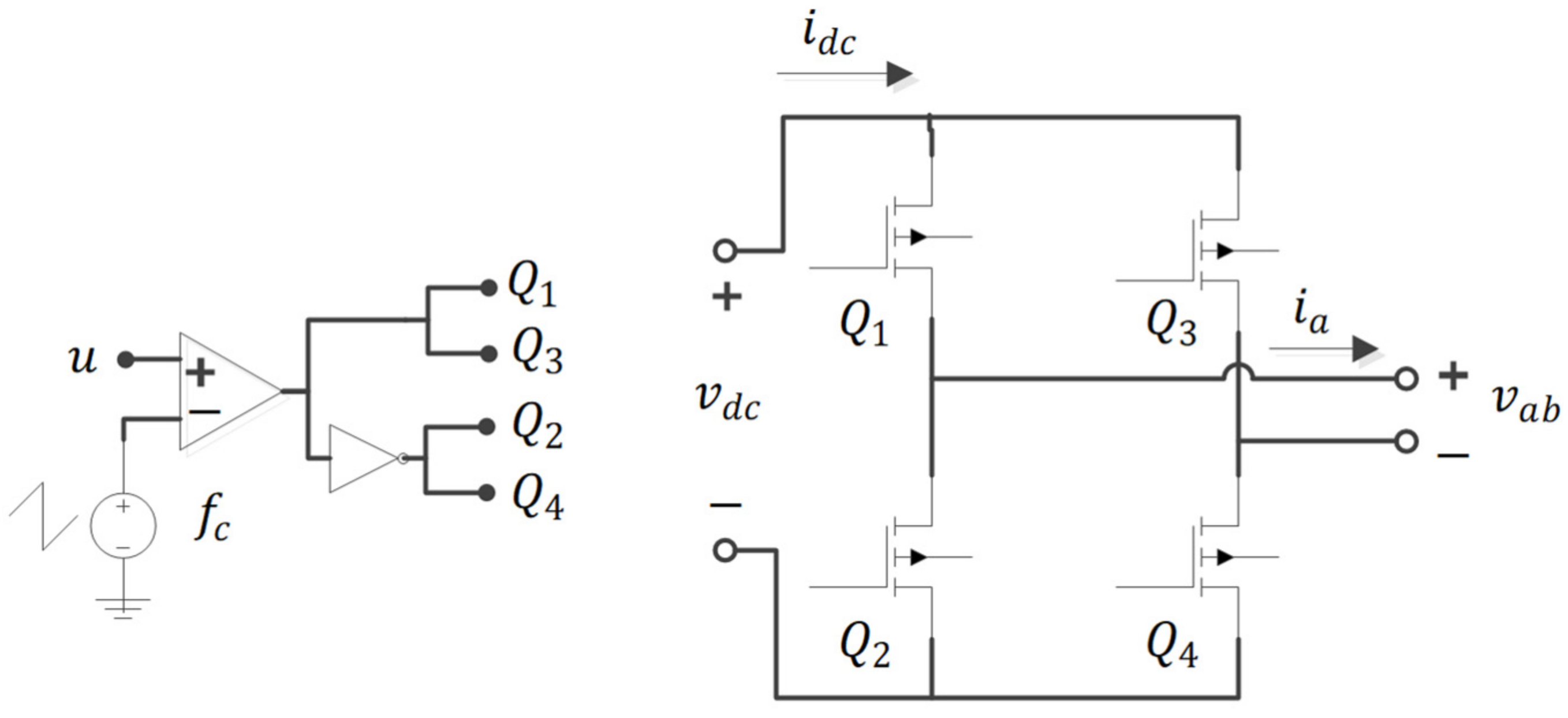
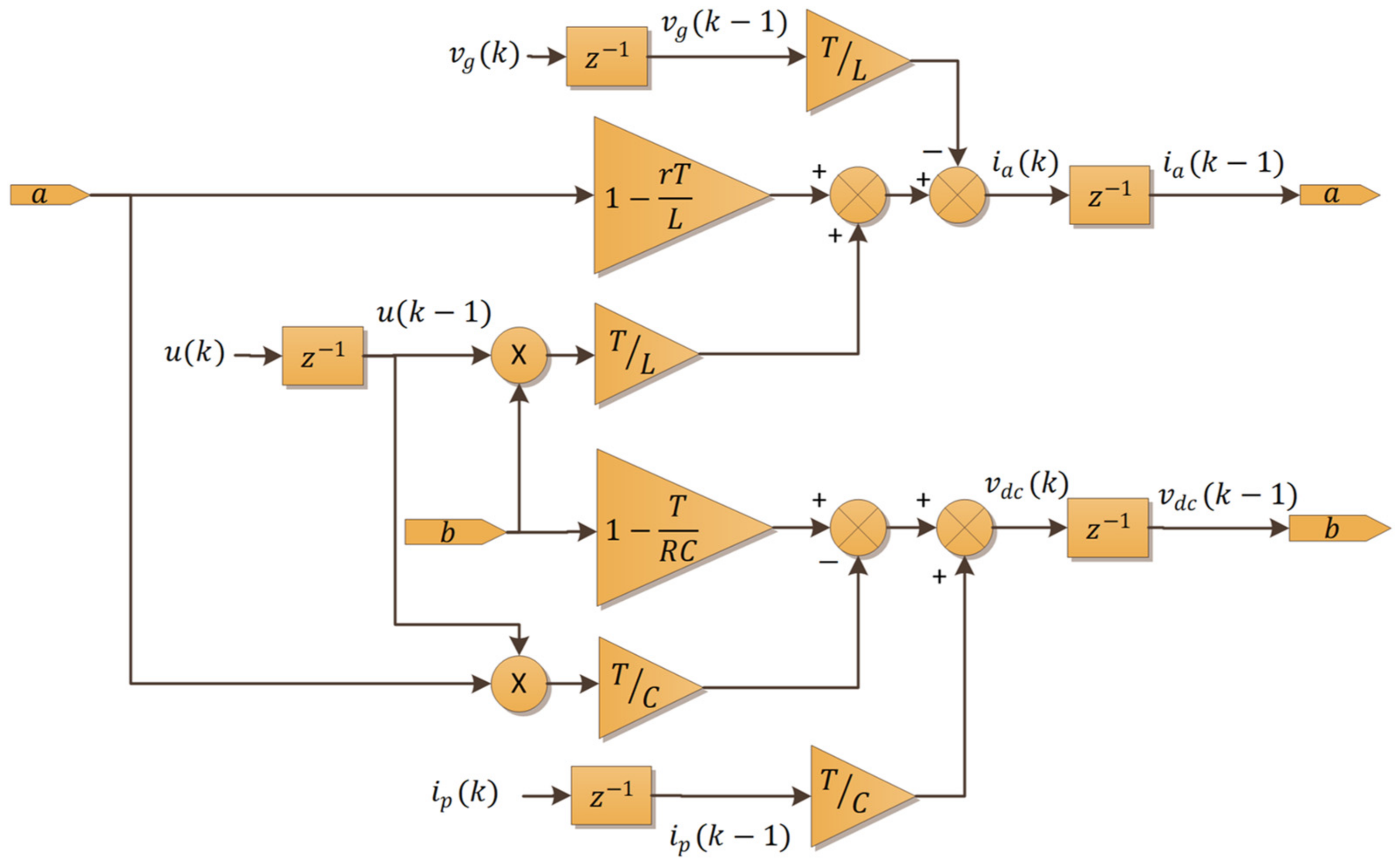
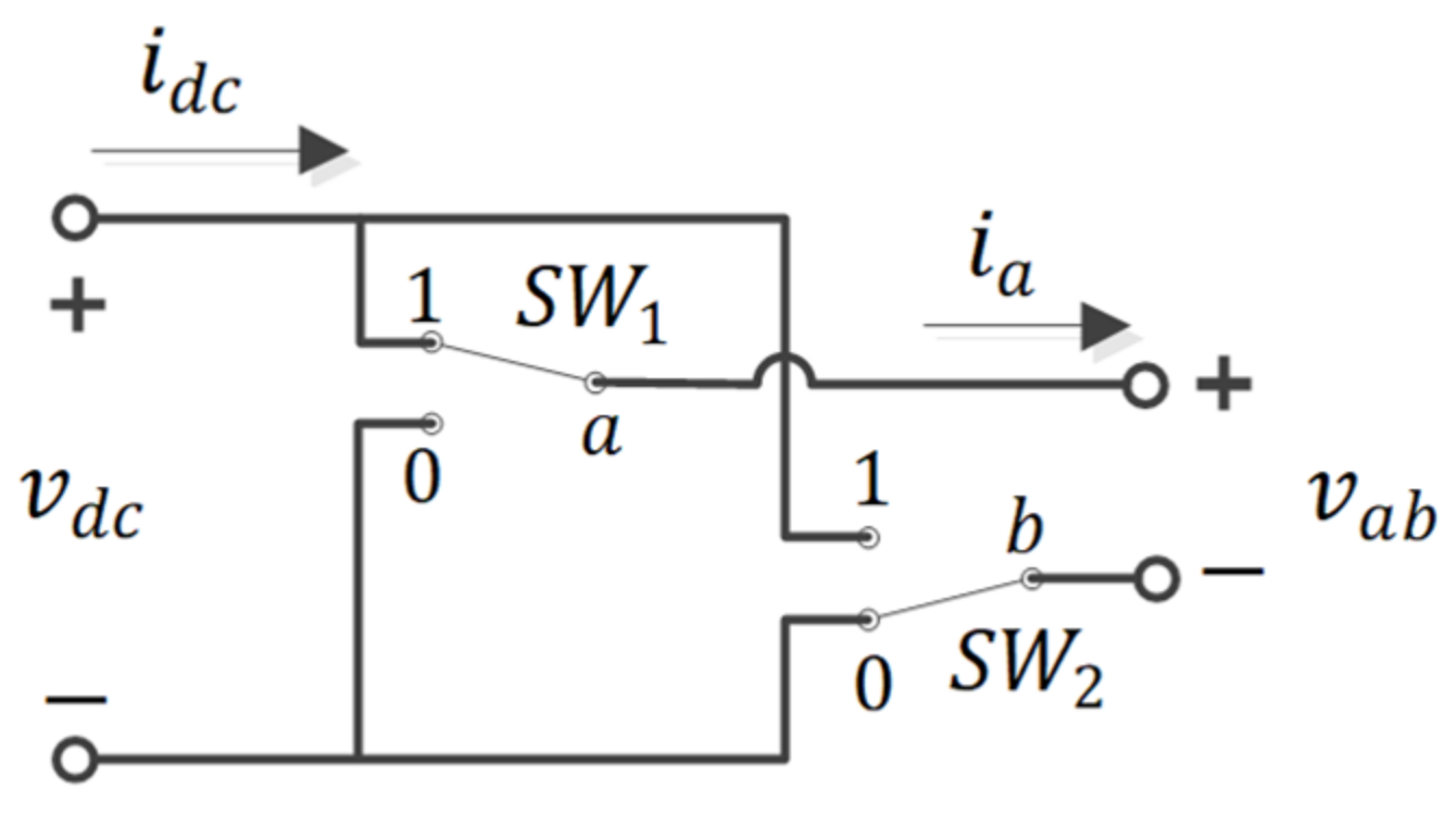
2.2. H Full Bridge Converter Description and Modeling
2.3. H Full Bridge Converter Design
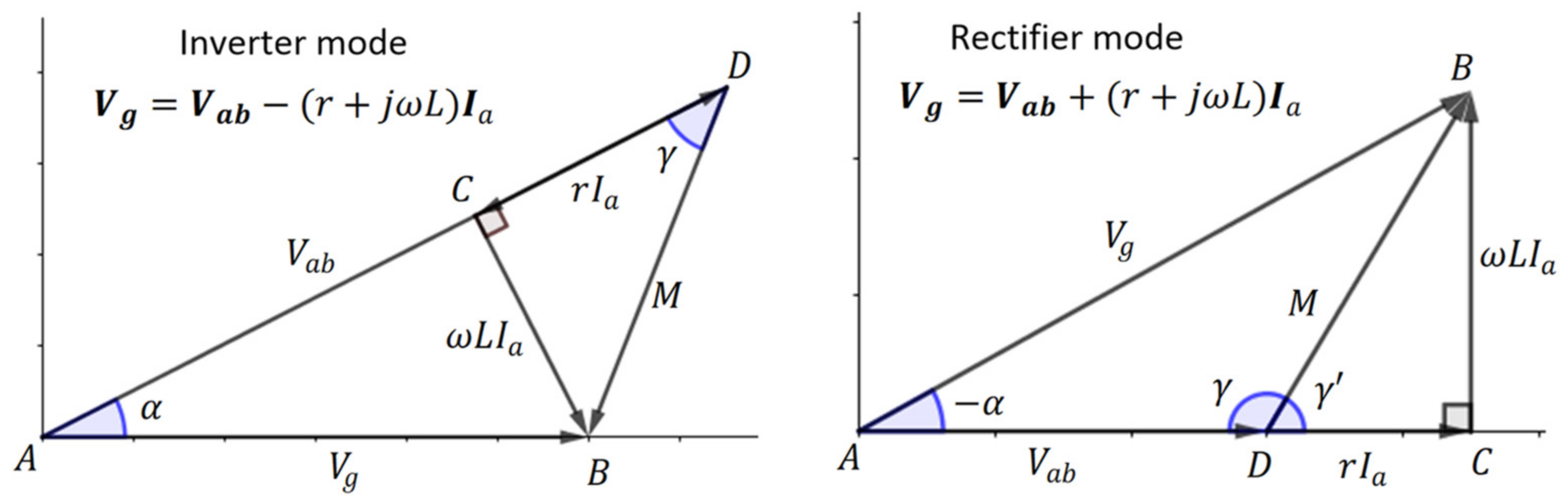
2.4. Open Loop Main Grid Interconnection System Response
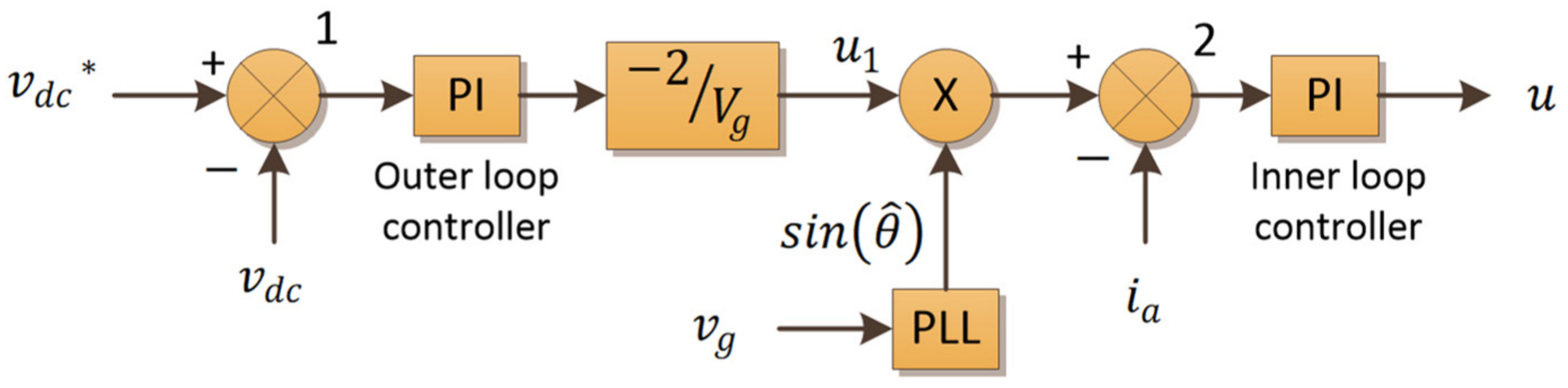
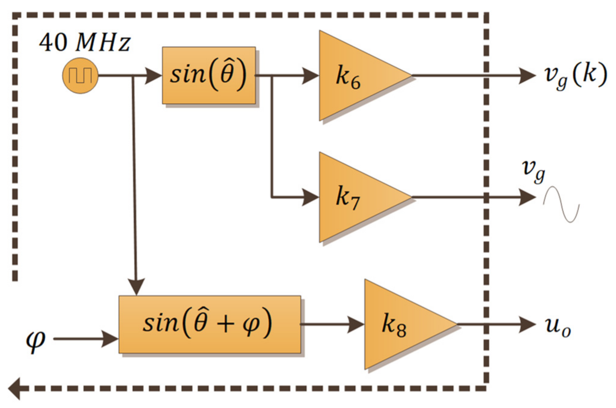
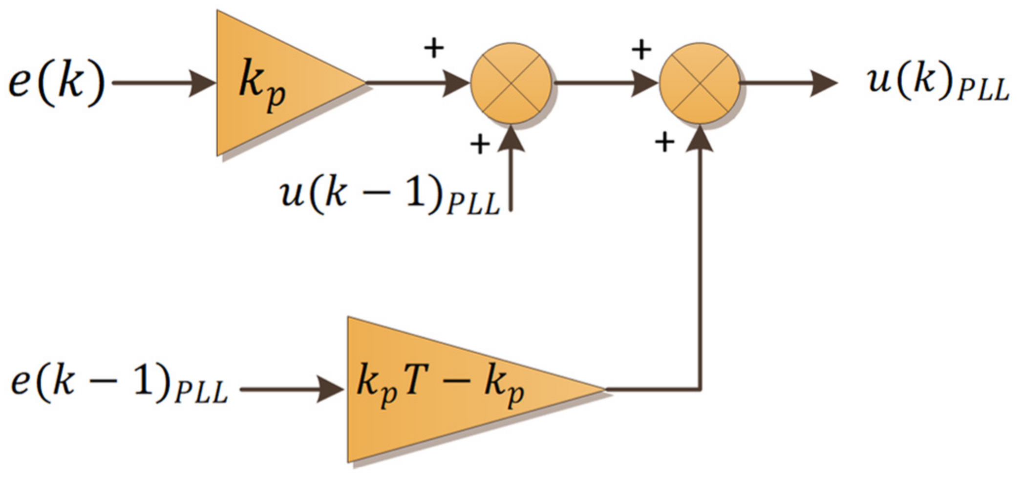
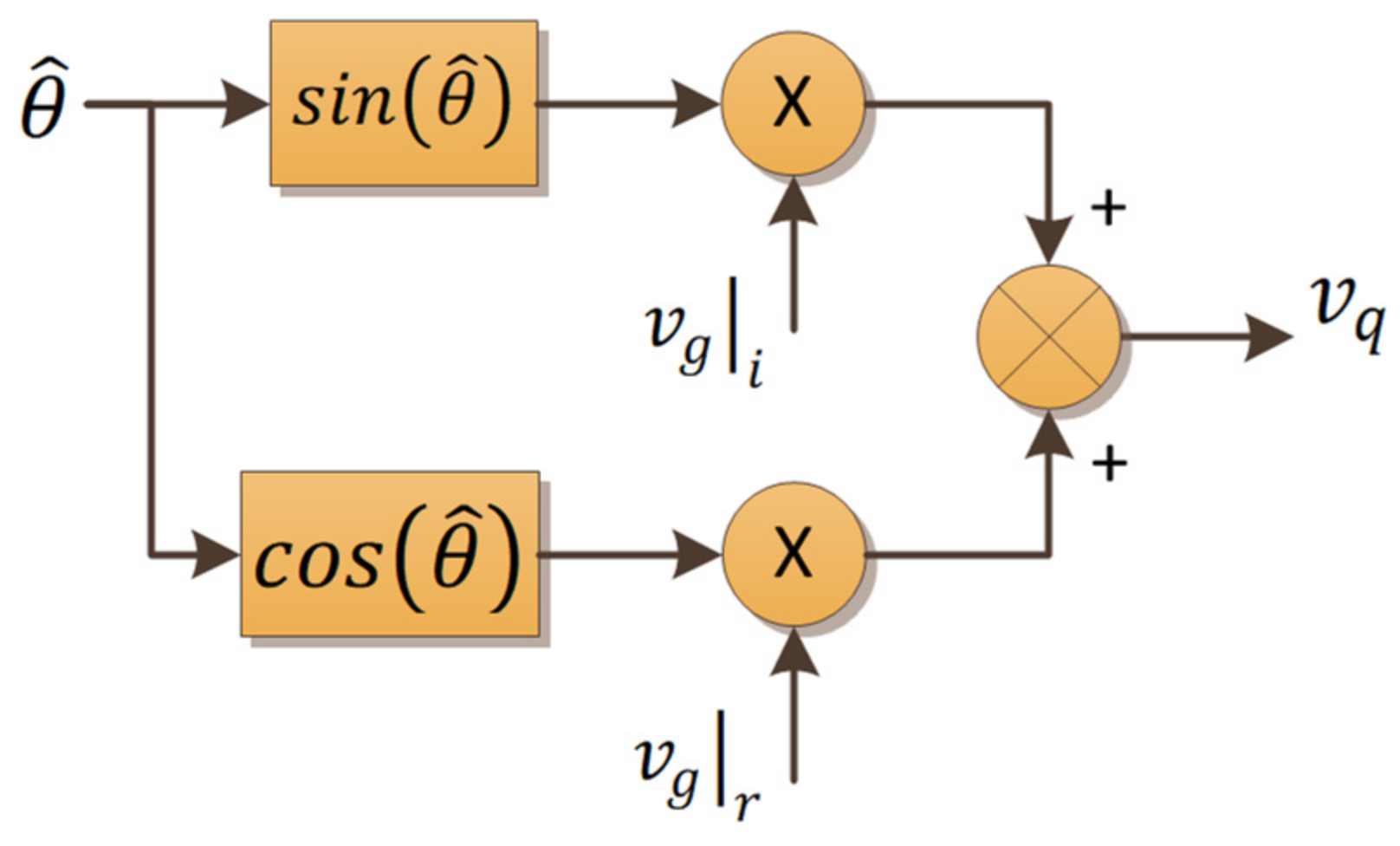
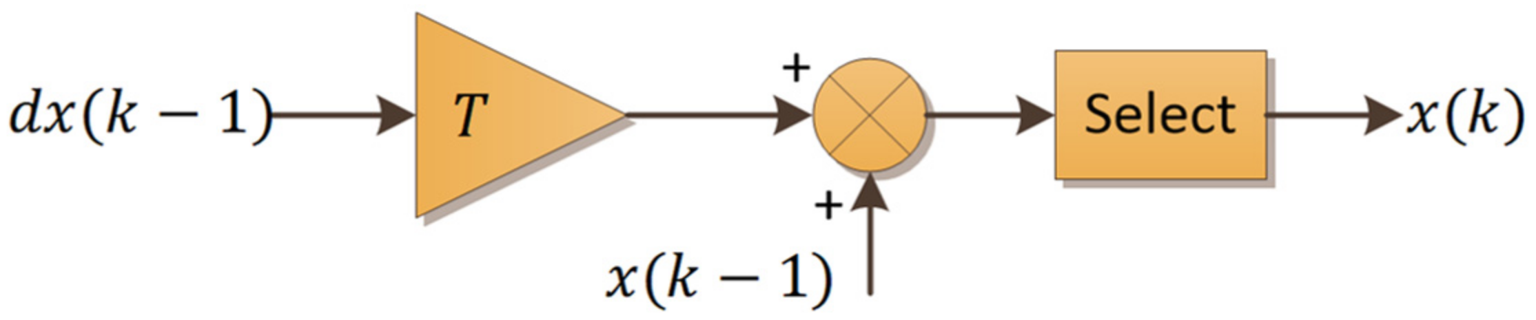
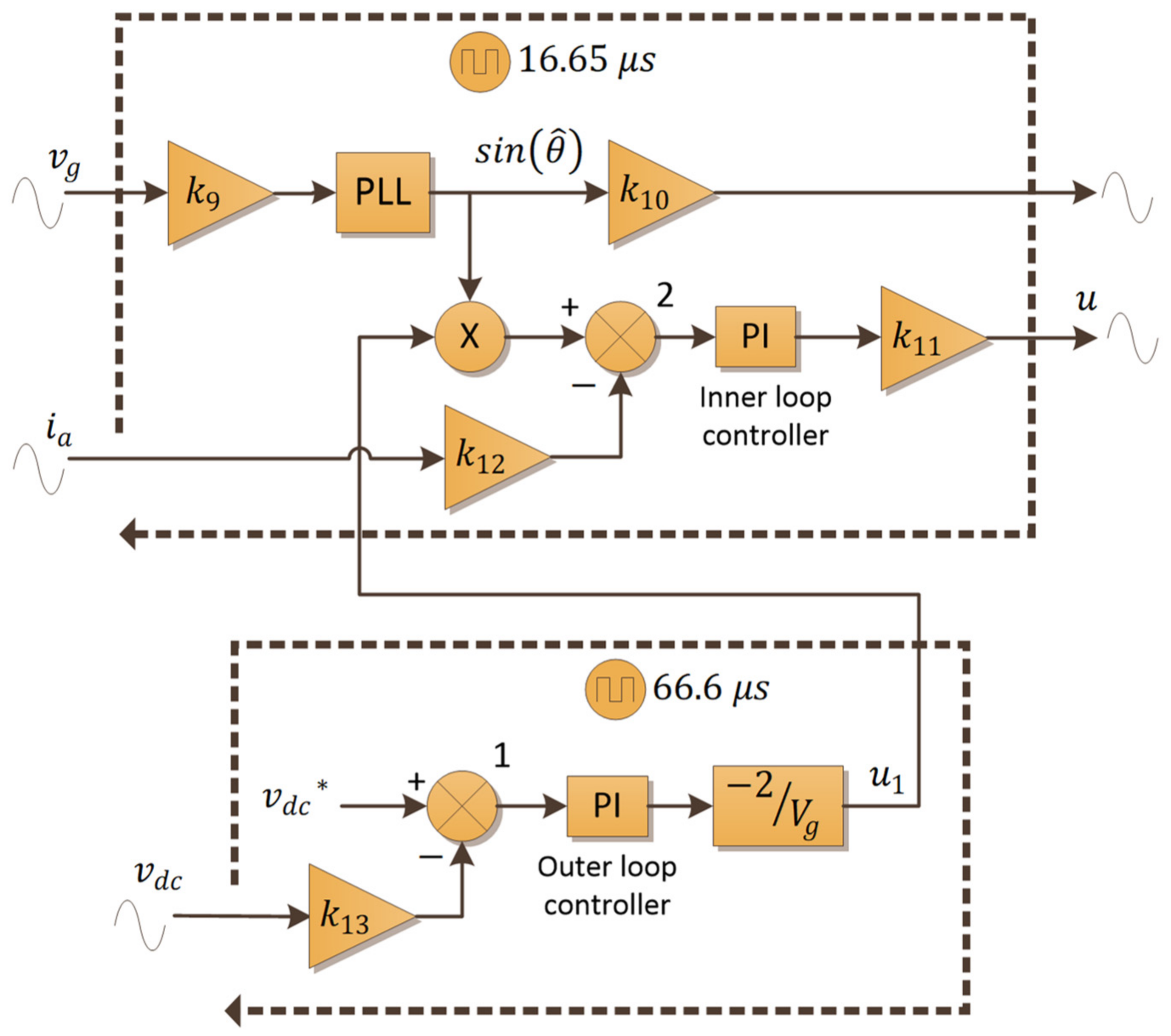
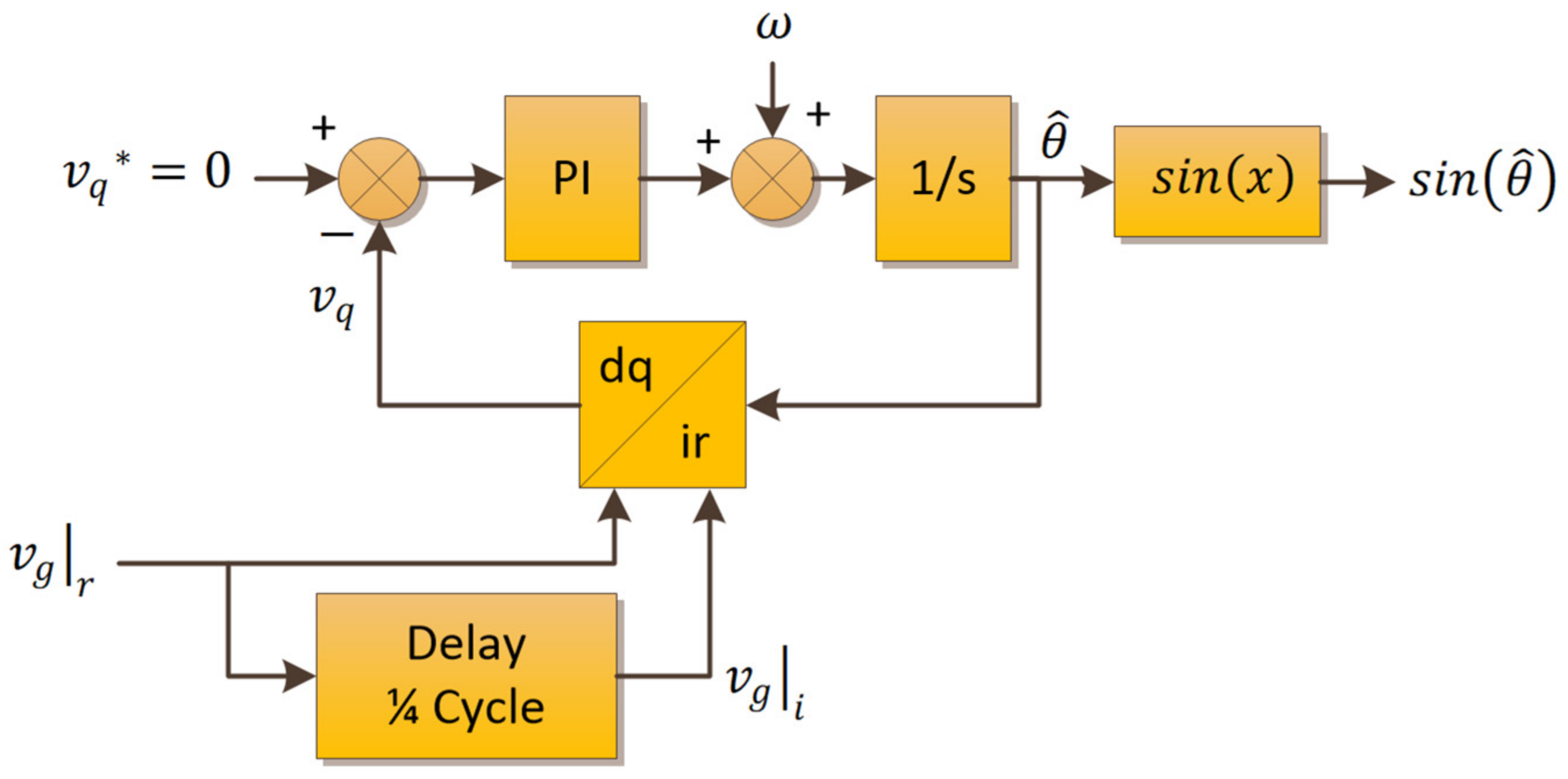
2.5. Controller Description
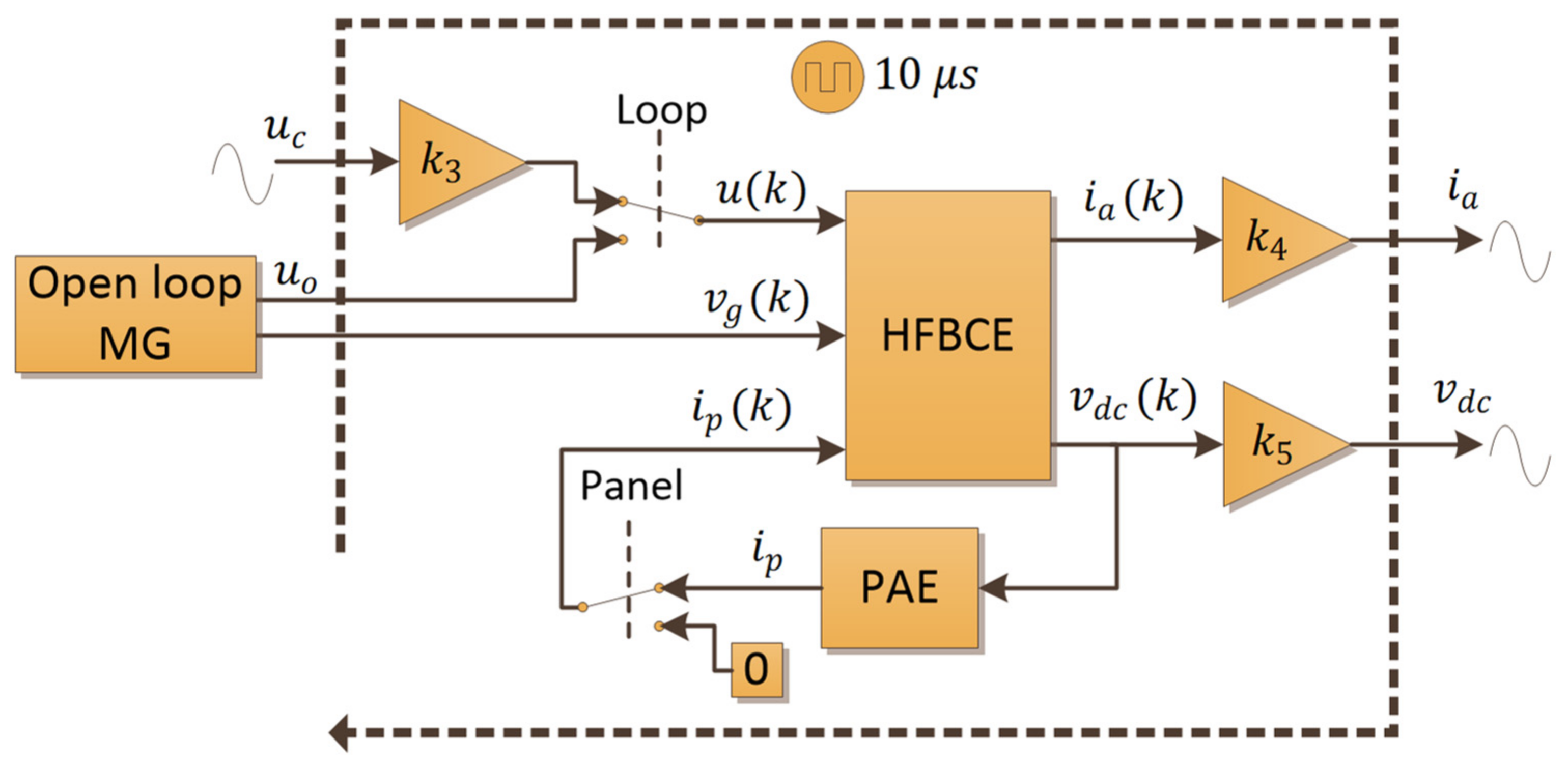
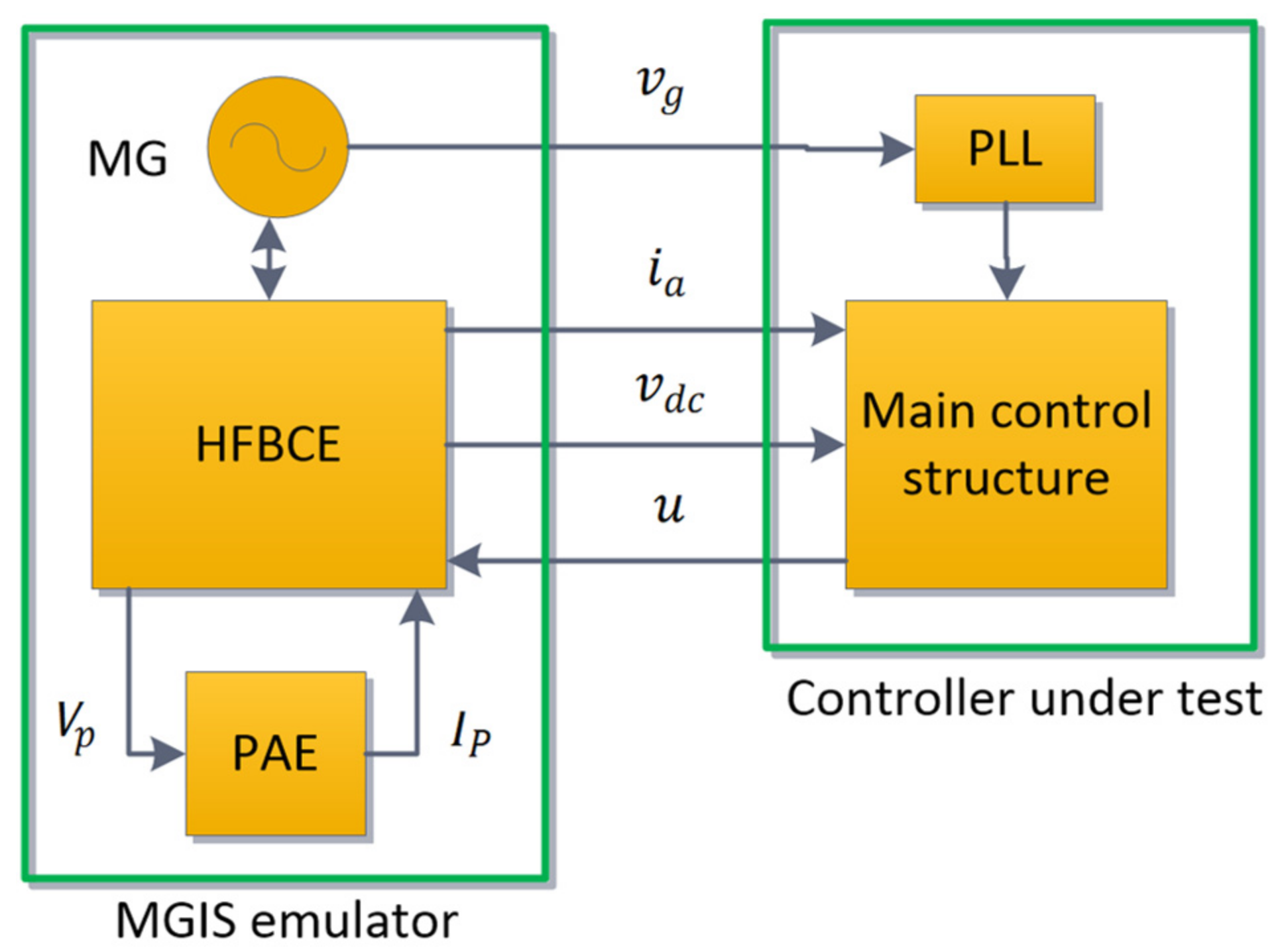
3. HIL Implementation
3.1. C-HIL Platform
3.2. Photovoltaic Array Emulator Implementation
3.3. H Full Bridge Converter Emulator Implementation
3.4. Main Grid Interconnection System Emulator Implementation
3.5. Open Loop
3.6. Main Grid Interconnection System Emulator Real Time Processor
3.7. Controller
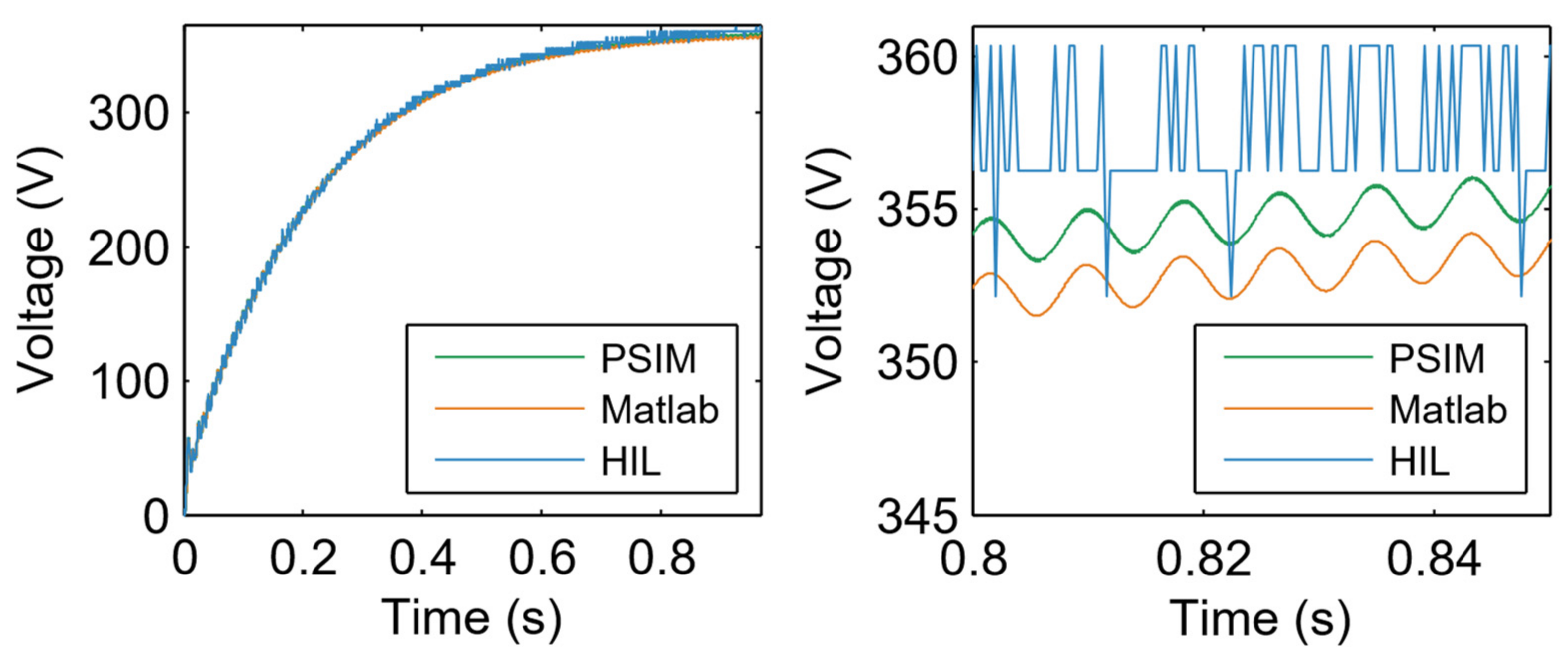
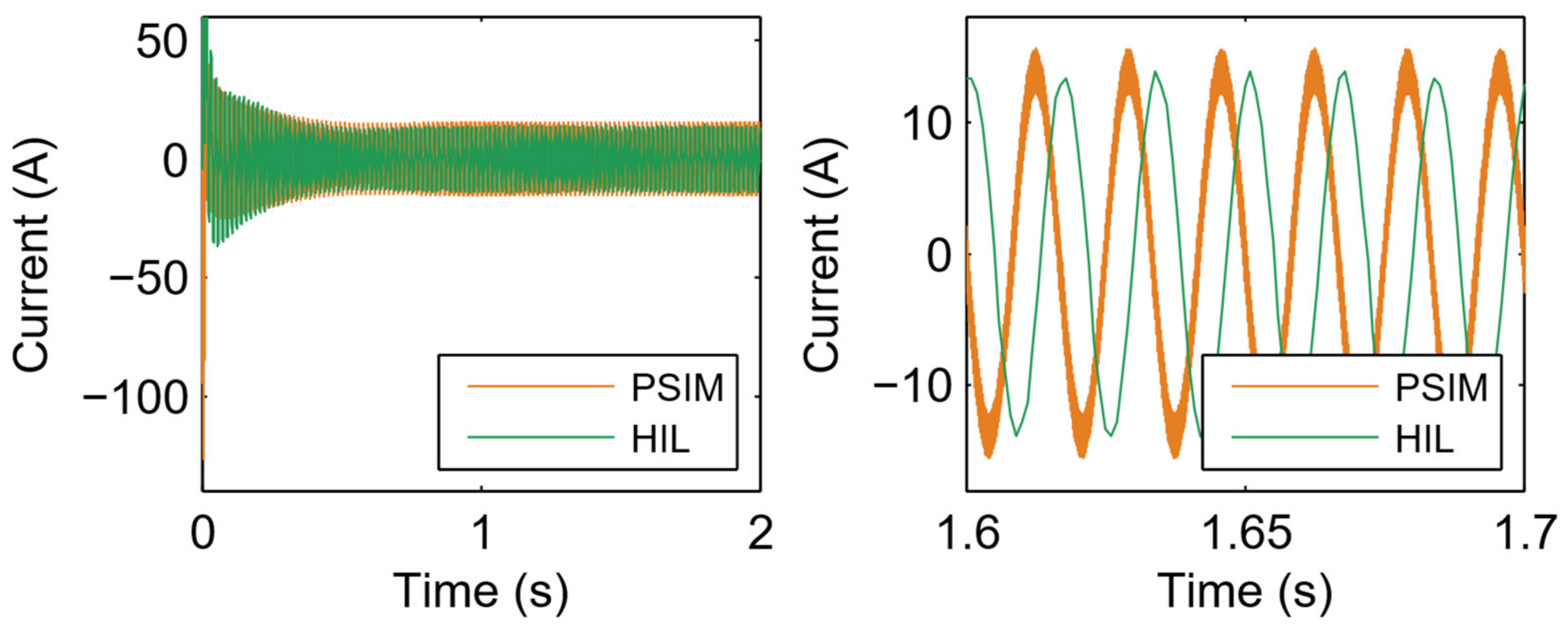
4. Results
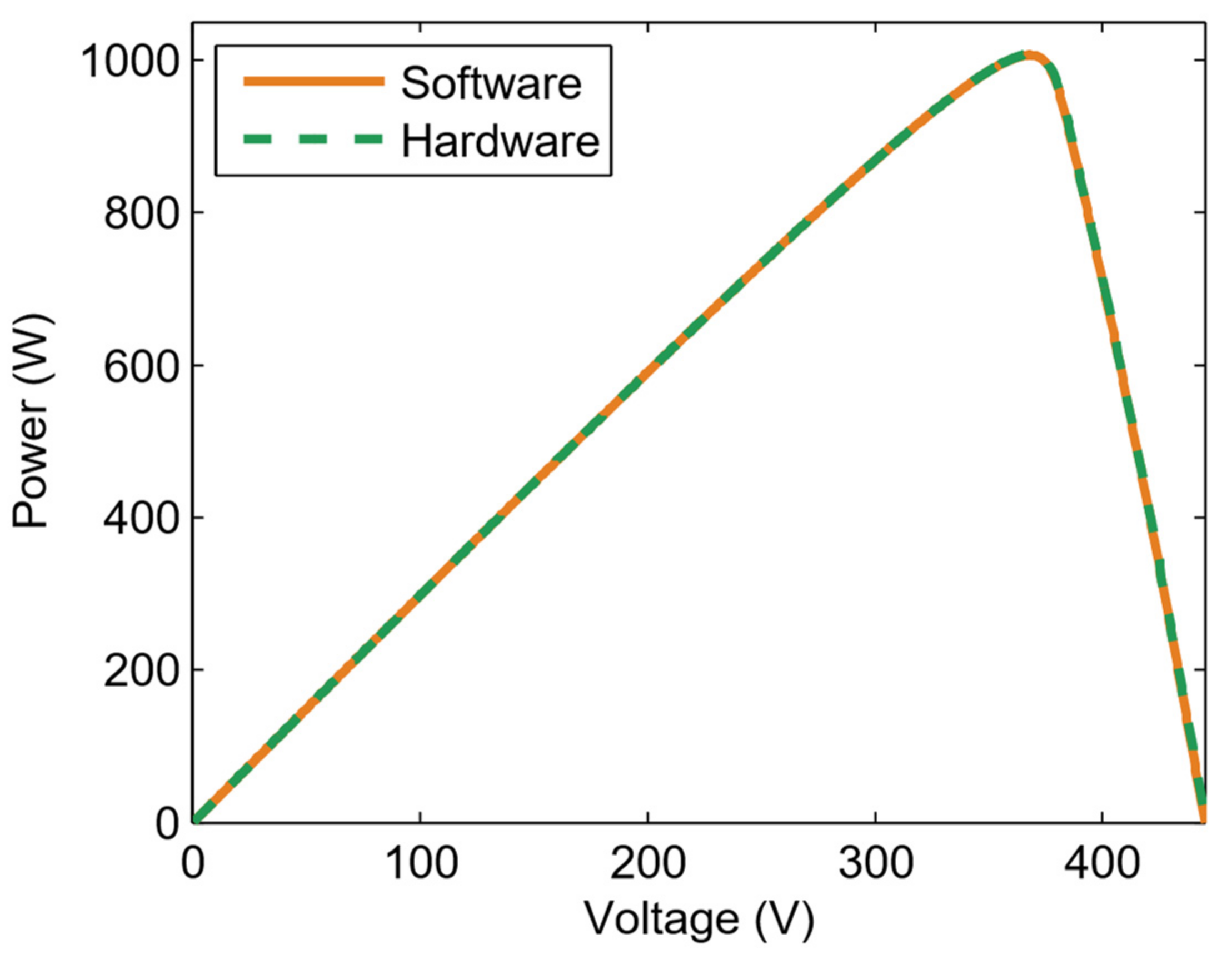
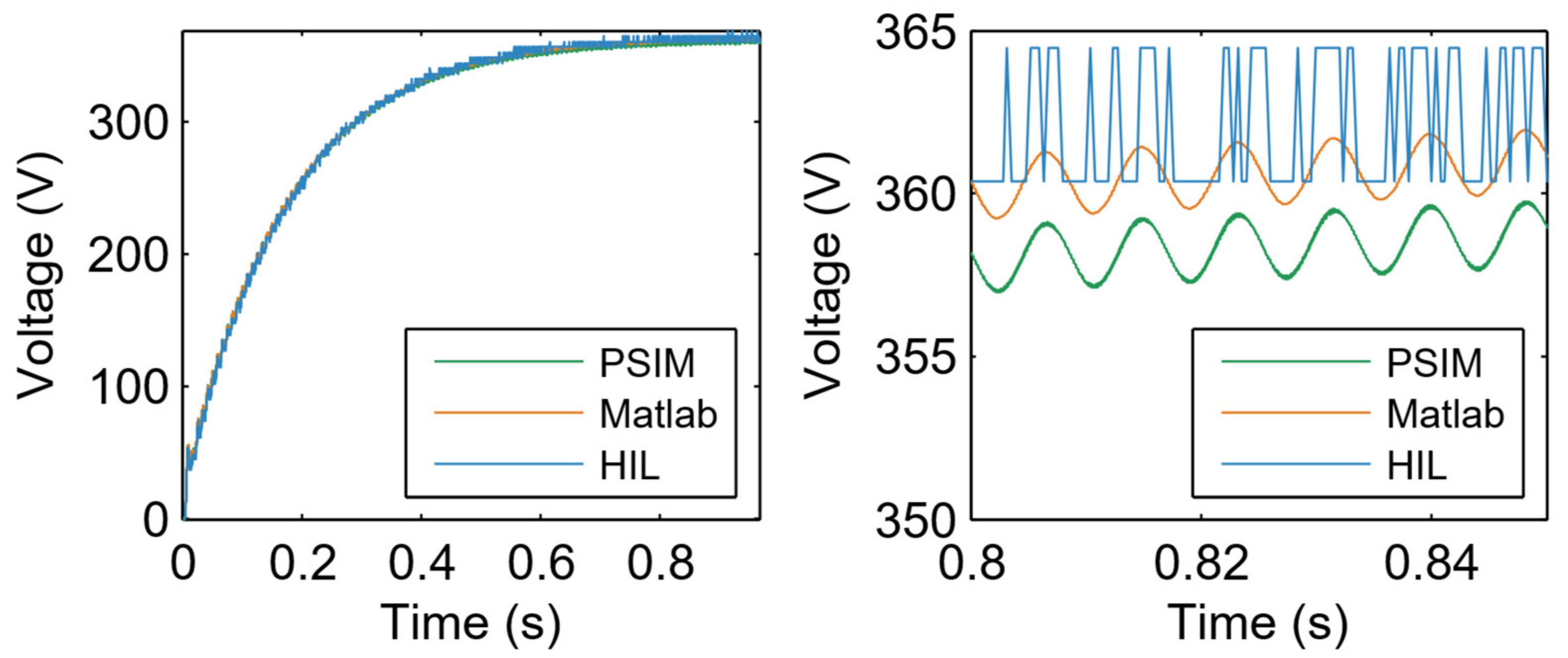
4.1. Photovoltaic Array
4.2. Open Loop Rectifier
4.3. Open Loop Inverter
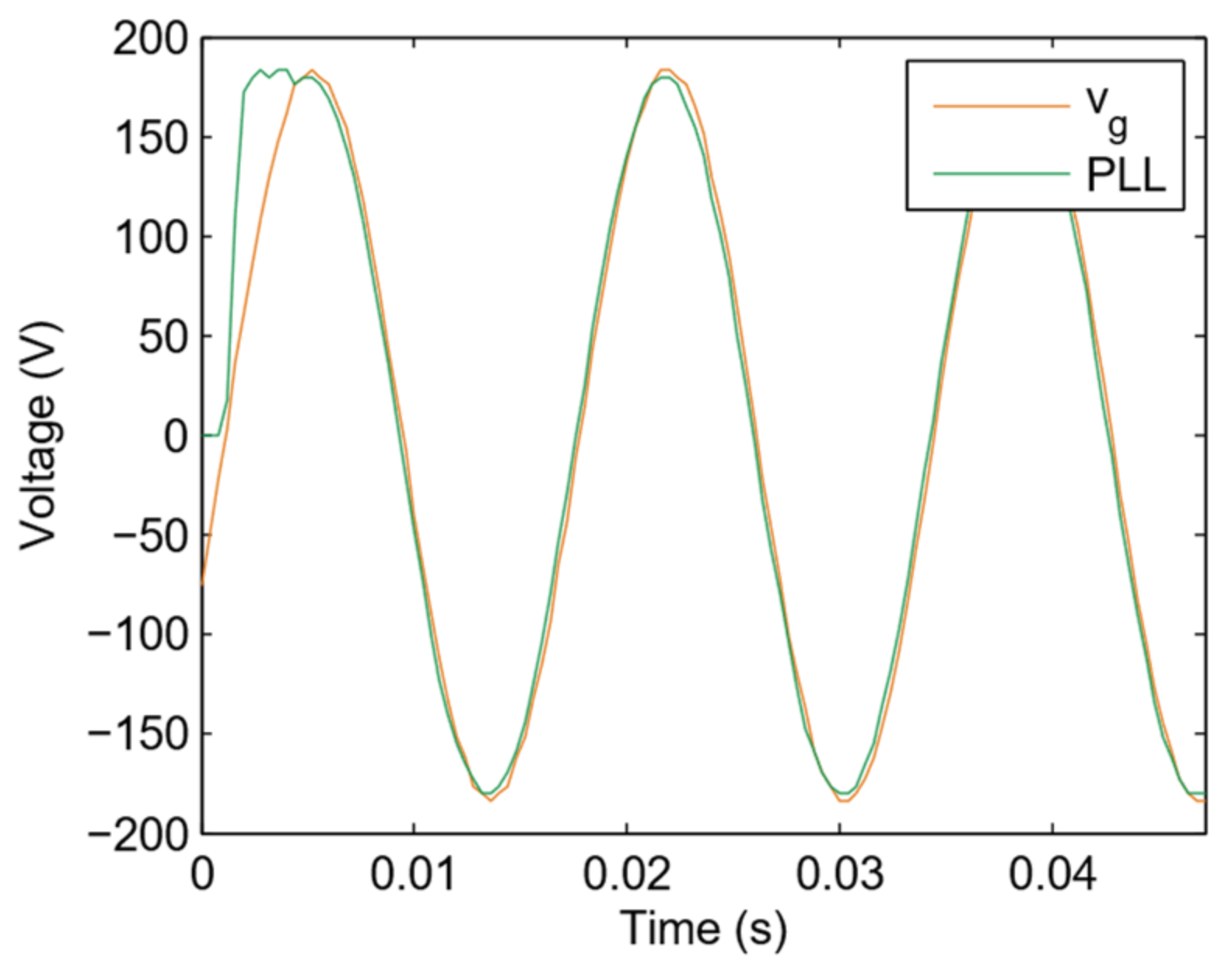
4.4. PLL
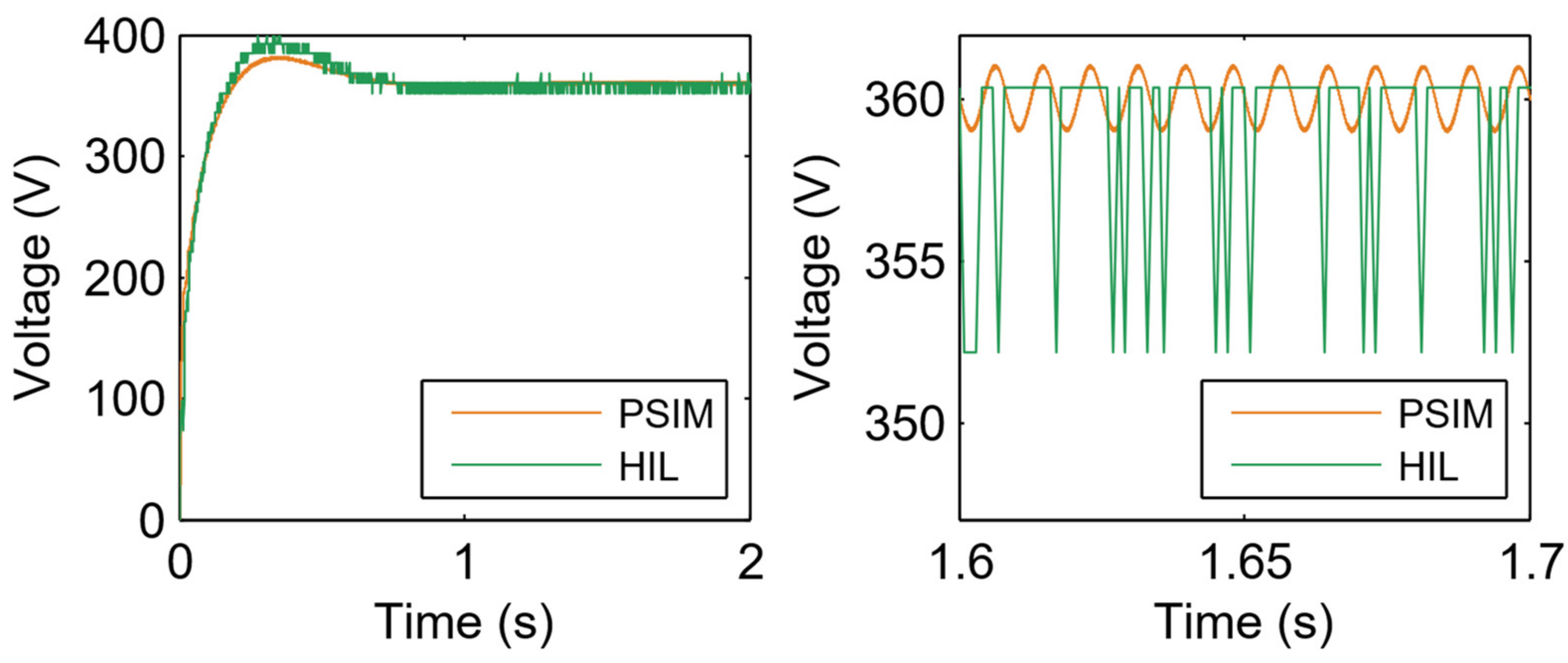
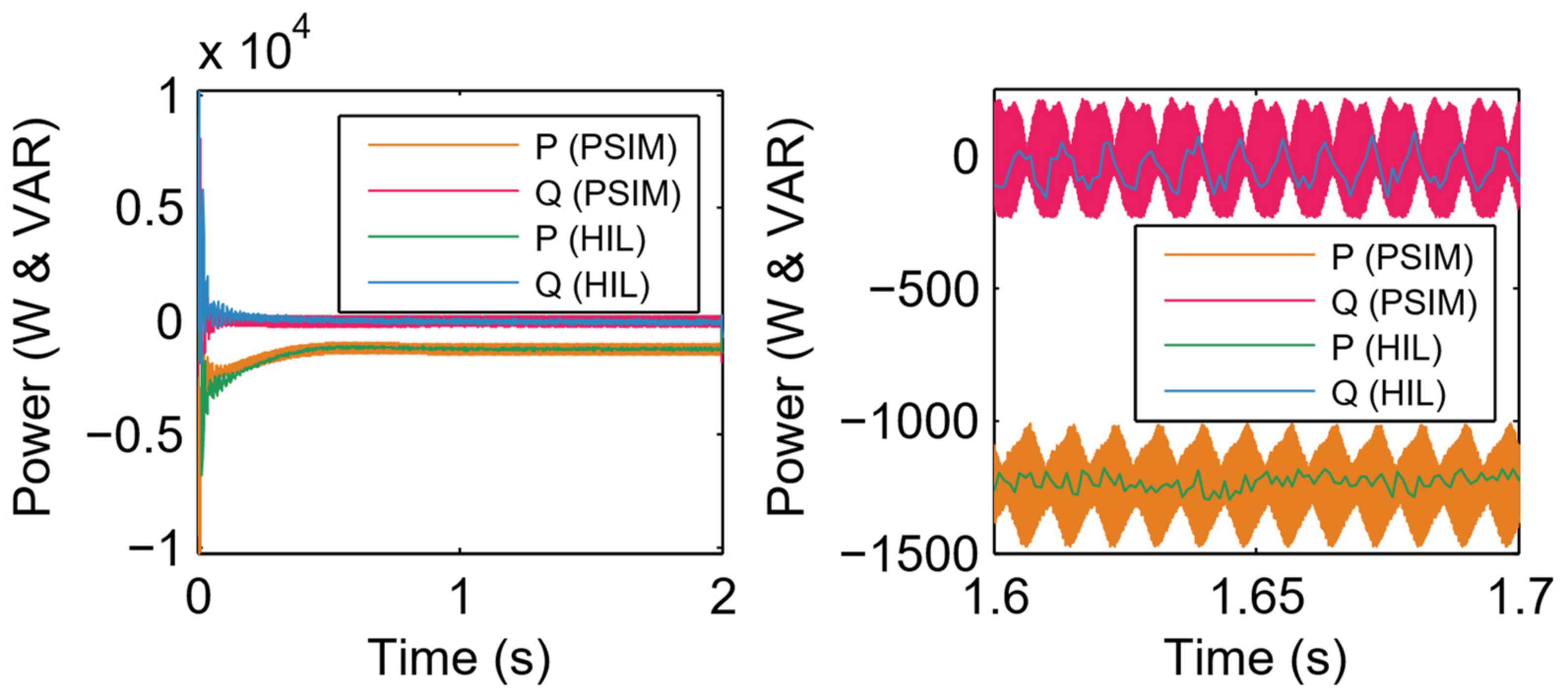
4.5. Closed Loop Rectifier
- Fundamental frequency : 60 Hz 13.85 Apk.
- Switching frequency : 9600 Hz 1.27 Apk, represents 9.22% of the fundamental peak value.
- High-frequency components: : 9480 Hz / 9720 Hz 0.112 Apk, represents 0.8% of the fundamental peak value; : 19140 Hz / 19260 Hz 0.1811 Apk, represents 1.3% of the fundamental peak value.
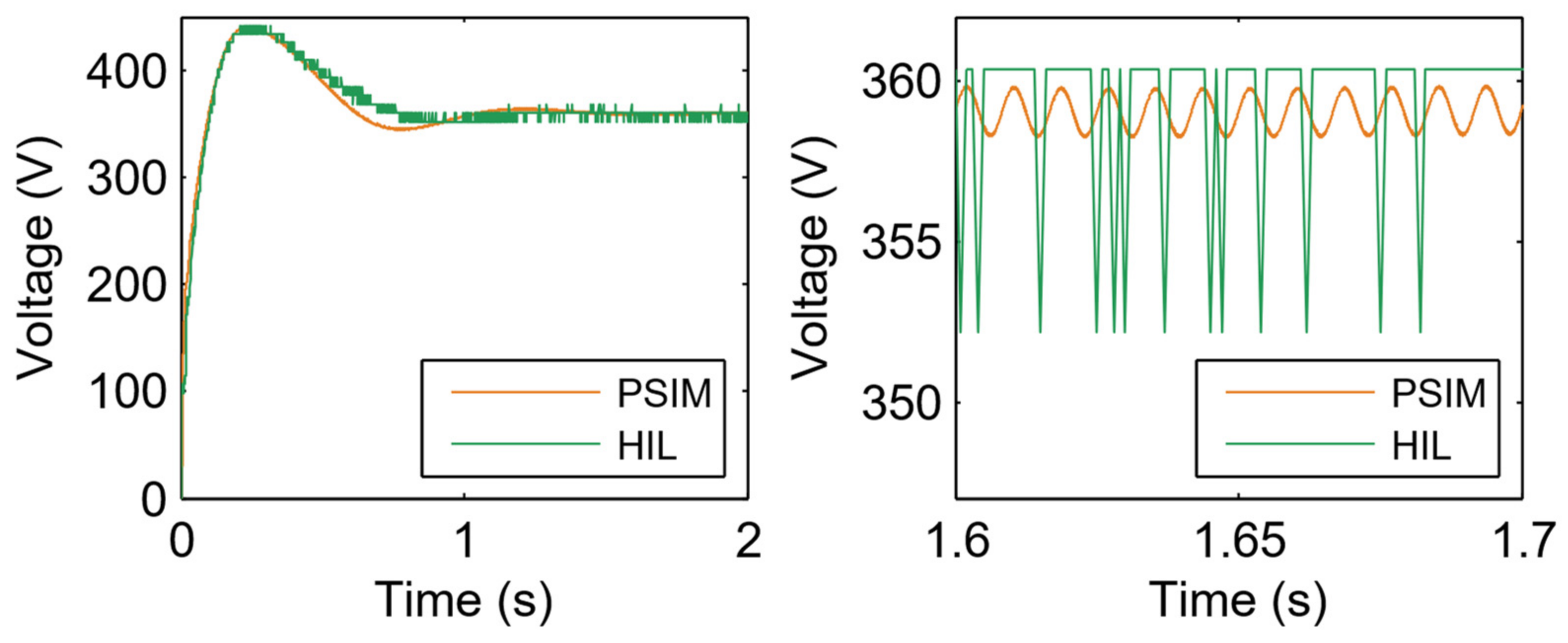
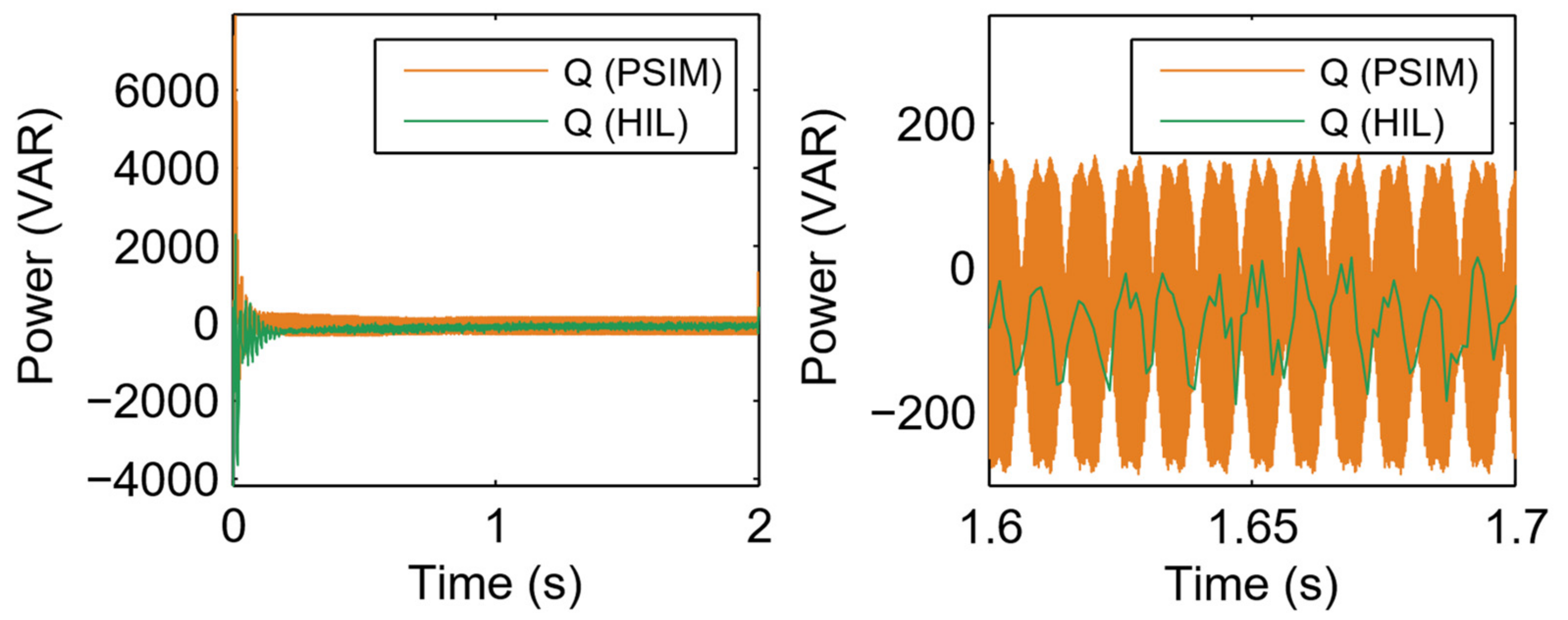
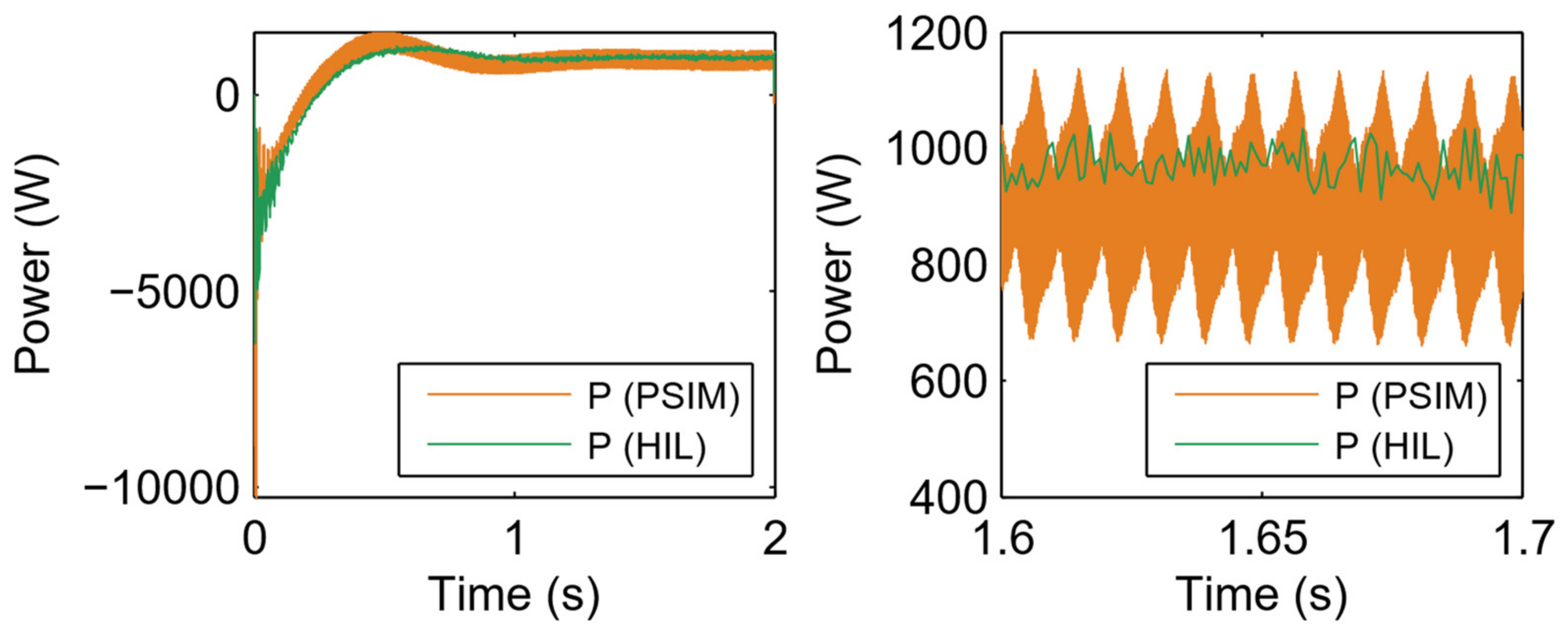
4.6. Closed Loop Inverter
- Fundamental component (): 60 Hz 10.00 Apk.
- Switching frequency (): 9600 Hz 1.31 Apk, represents 13.1% of the fundamental frequency peak value.
- High-frequency components: : 9480 Hz / 9720 Hz 0.1376 Apk, represents 1.37% of the fundamental frequency peak value; : 19140 Hz / 19260 Hz 0.17 Apk, represents 1.7% of the fundamental frequency peak value.
5. Conclusions
Author Contributions
Funding
Institutional Review Board Statement
Informed Consent Statement
Data Availability Statement
Conflicts of Interest
References
- Yao, S.; Zhang, S.; Zhang, X. Renewable energy, carbon emission and economic growth: A revised environmental Kuznets Curve perspective. J. Clean. Prod. 2019, 235, 1338–1352. [Google Scholar] [CrossRef]
- Hirsch, A.; Parag, Y.; Guerrero, J. Microgrids: A review of technologies, key drivers, and outstanding issues. Renew. Sustain. Energy Rev. 2018, 90, 402–411. [Google Scholar] [CrossRef]
- Pannala, S.; Patari, N.; Srivastava, A.K.; Padhy, N.P. Effective Control and Management Scheme for Isolated and Grid Connected DC Microgrid. IEEE Trans. Ind. Appl. 2020, 56, 6767–6780. [Google Scholar] [CrossRef]
- Rana, M.J.; Abido, M.A. Energy management in DC microgrid with energy storage and model predictive controlled AC–DC converter. IET Gener. Transm. Distrib. 2017, 11, 3694–3702. [Google Scholar] [CrossRef]
- Wang, Y.; Nguyen, T.L.; Xu, Y.; Tran, Q.T.; Caire, R. Peer-to-peer control for networked microgrids: Multi-layer and multi-agent architecture design. IEEE Trans. Smart Grid 2020, 11, 4688–4699. [Google Scholar] [CrossRef]
- Shi, D.; Lin, P.; Wang, Y.; Chu, C.C.; Xu, Y.; Wang, P. Deception Attack Detection of Isolated DC Microgrids Under Consensus-Based Distributed Voltage Control Architecture. IEEE J. Emerg. Sel. Top. Circuits Syst. 2021, 11, 155–167. [Google Scholar] [CrossRef]
- Vigneysh, T.; Kumarappan, N. Grid interconnection of renewable energy sources using multifunctional grid-interactive converters: A fuzzy logic based approach. Electr. Power Syst. Res. 2017, 151, 359–368. [Google Scholar] [CrossRef]
- Šimek, P.; Valouch, V. Generalized predictive power control for grid-connected converter. Int. J. Electr. Power Energy Syst. 2021, 125, 106380. [Google Scholar] [CrossRef]
- Aryani, D.R.; Kim, J.S.; Song, H. Interlink converter with linear quadratic regulator based current control for hybrid AC/DC microgrid. Energies 2017, 10, 1799. [Google Scholar] [CrossRef] [Green Version]
- Shan, Y.; Hu, J.; Chan, K.W.; Fu, Q.; Guerrero, J.M. Model Predictive Control of Bidirectional DC–DC Converters and AC/DC Interlinking Converters—A New Control Method for PV-Wind-Battery Microgrids. IEEE Trans. Sustain. Energy 2019, 10, 1823–1833. [Google Scholar] [CrossRef]
- Li, P.; Guo, T.; Zhou, F.; Yang, J.; Liu, Y. Nonlinear coordinated control of parallel bidirectional power converters in an AC/DC hybrid microgrid. Int. J. Electr. Power Energy Syst. 2020, 122, 106208. [Google Scholar] [CrossRef]
- Zheng, X.; Gao, F.; Ali, H.; Liu, H. A Droop Control Based Three Phase Bidirectional AC-DC Converter for More Electric Aircraft Applications. Energies 2017, 10, 400. [Google Scholar] [CrossRef] [Green Version]
- Shen, X.; Tan, D.; Shuai, Z.; Luo, A. Control Techniques for Bidirectional Interlinking Converters in Hybrid Microgrids: Leveraging the advantages of both ac and dc. IEEE Power Electron. Mag. 2019, 6, 39–47. [Google Scholar] [CrossRef]
- Lu, B.; Wu, X.; Figueroa, H.; Monti, A. A low-cost real-time hardware-in-the-loop testing approach of power electronics controls. IEEE Trans. Ind. Electron. 2007, 54, 919–931. [Google Scholar] [CrossRef]
- Oh, Y.J.; Lee, J.K.; Liu, H.C.; Cho, S.; Lee, J.; Lee, H.J. Hardware-in-the-Loop Simulation for active control of tramcars with independently rotating wheels. IEEE Access 2019, 7, 71252–71261. [Google Scholar] [CrossRef]
- Hogan, D.; Albiol-Tendillo, L.; Kelleher, B.; Valdivia-Guerrero, V.; Foley, R. Rapid-prototyping and hardware-in-the-loop laboratory platform for development and testing of electro-mechanical actuator controls. J. Eng. 2019, 2019, 4133–4137. [Google Scholar] [CrossRef]
- Wang, Q.; Liu, Z.; Tang, Y. Design of a Co-Simulation Platform with Hardware-in-the-Loop for Cyber-attacks on Cyber-Physical Power Systems. In Proceedings of the 2019 IEEE 9th Annual International Conference on CYBER Technology in Automation, Control, and Intelligent Systems (CYBER), Suzhou, China, 29 July–2 August 2019; pp. 430–434. [Google Scholar] [CrossRef]
- De Farias, A.B.C.; Rodrigues, R.S.; Murilo, A.; Lopes, R.V.; Avila, S. Low-cost hardware-in-the-loop platform for embedded control strategies simulation. IEEE Access 2019, 7, 111499–111512. [Google Scholar] [CrossRef]
- Bastos, R.F.; Silva, F.B.; Aguiar, C.R.; Fuzato, G.; Machado, R.Q. Low-cost hardware-in-the-loop for real-time simulation of electric machines and electric drive. IET Electr. Power Appl. 2020, 14, 1679–1685. [Google Scholar] [CrossRef]
- Goni, O.; Sanchez, A.; Todorovich, E.; de Castro, A. Resolution analysis of switching converter models for hardware-in-the-loop. IEEE Trans. Ind. Inform. 2013, 10, 1162–1170. [Google Scholar] [CrossRef]
- Tian, J.; Liu, J.; Shu, J.; Tang, J.; Yang, J. Engineering modelling of wind turbine applied in real-time simulation with hardware-in-loop and optimising control. IET Power Electron. 2018, 11, 2490–2498. [Google Scholar] [CrossRef]
- Moussa, I.; Bouallegue, A.; Khedher, A. New wind turbine emulator based on DC machine: Hardware implementation using FPGA board for an open-loop operation. IET Circuits Devices Syst. 2019, 13, 896–902. [Google Scholar] [CrossRef]
- Ye, Q.; Mo, R.; Li, H. Low-frequency resonance suppression of a dual-active-bridge DC/DC converter enabled DC microgrid. IEEE J. Emerg. Sel. Top. Power Electron. 2017, 5, 982–994. [Google Scholar] [CrossRef]
- Doroudchi, E.; Feng, X.; Strank, S.; Hebner, R.E.; Kyyrä, J. Hardware-in-the-loop test for real-time economic control of a DC microgrid. J. Eng. 2019, 2019, 4298–4303. [Google Scholar] [CrossRef]
- Broadmeadow, M.A.H.; Walker, G.R.; Ledwich, G.F. Modular and scalable control and data acquisition system for power hardware in the loop (PHIL) amplifiers. J. Eng. 2019, 2019, 3655–3659. [Google Scholar] [CrossRef]
- Maniatopoulos, M.; Lagos, D.; Kotsampopoulos, P.; Hatziargyriou, N. Combined control and power hardware in-the-loop simulation for testing smart grid control algorithms. IET Gener. Transm. Distrib. 2017, 11, 3009–3018. [Google Scholar] [CrossRef]
- Li, G.; Zhang, D.; Xin, Y.; Jiang, S.; Wang, W.; Du, J. Design of MMC hardware-in-the-loop platform and controller test scheme. CPSS Trans. Power Electron. Appl. 2019, 4, 143–151. [Google Scholar] [CrossRef]
- Bai, H.; Liu, C.; Zhuo, S.; Ma, R.; Paire, D.; Gao, F. FPGA-based device-level electro-thermal modeling of floating interleaved boost converter for fuel cell hardware-in-the-loop applications. IEEE Trans. Ind. Appl. 2019, 55, 5300–5310. [Google Scholar] [CrossRef]
- Kong, L.; Nian, H. Transient Modeling Method for Faulty DC Microgrid Considering Control Effect of DC/AC and DC/DC Converters. IEEE Access 2020, 8, 150759–150772. [Google Scholar] [CrossRef]
- Ghanbari, N.; Bhattacharya, S. Adaptive Droop Control Method for Suppressing Circulating Currents in DC Microgrids. IEEE Open Access J. Power Energy 2020, 7, 100–110. [Google Scholar] [CrossRef]
- Hassan, M.A.; He, Y. Constant Power Load Stabilization in DC Microgrid Systems Using Passivity-Based Control with Nonlinear Disturbance Observer. IEEE Access 2020, 8, 92393–92406. [Google Scholar] [CrossRef]
- Jeung, Y.C.; Le, D.D.; Lee, D.C. Analysis and design of DC-bus voltage controller of energy storage systems in DC microgrids. IEEE Access 2019, 7, 126696–126708. [Google Scholar] [CrossRef]
- Liu, H.; Guo, W.; Cheng, D.; Wang, Y.; Wang, M. Stability and Bifurcation Analysis of DC Microgrid With Multiple Droop Control Sources and Loads. IEEE Trans. Power Electron. 2020, 36, 2361–2372. [Google Scholar] [CrossRef]
- Meng, J.; Wang, Y.; Wang, C.; Wang, H. Design and implementation of hardware-in-the-loop simulation system for testing control and operation of DC microgrid with multiple distributed generation units. IET Gener. Transm. Distrib. 2017, 11, 3065–3072. [Google Scholar] [CrossRef]
- Peng, D.; Huang, M.; Li, J.; Sun, J.; Zha, X.; Wang, C. Large-signal stability criterion for parallel-connected DC–DC converters with current source equivalence. IEEE Trans. Circuits Syst. II Express Briefs 2019, 66, 2037–2041. [Google Scholar] [CrossRef]
- Mardani, M.M.; Vafamand, N.; Khooban, M.H.; Dragičević, T.; Blaabjerg, F. Design of quadratic D-stable fuzzy controller for DC microgrids with multiple CPLs. IEEE Trans. Ind. Electron. 2018, 66, 4805–4812. [Google Scholar] [CrossRef] [Green Version]
- Syed, M.H.; Guillo-Sansano, E.; Wang, Y.; Vogel, S.; Palensky, P.; Burt, G.M.; Xu, Y.; Monti, A.; Hovsapian, R. Real-Time Coupling of Geographically Distributed Research Infrastructures: Taxonomy, Overview and Real-World Smart Grid Applications. IEEE Trans. Smart Grid 2020, 12, 1747–1760. [Google Scholar] [CrossRef]
- Salcedo, R.; Corbett, E.; Smith, C.; Limpaecher, E.; Rekha, R.; Nowocin, J.; Lauss, G.; Fonkwe, E.; Almeida, M.; Gartner, P.; et al. Banshee distribution network benchmark and prototyping platform for hardware-in-the-loop integration of microgrid and device controllers. J. Eng. 2019, 2019, 5365–5373. [Google Scholar] [CrossRef]
- Kleftakis, V.; Lagos, D.; Papadimitriou, C.; Hatziargyriou, N.D. Seamless transition between interconnected and islanded operation of DC Microgrids. IEEE Trans. Smart Grid 2017, 10, 248–256. [Google Scholar] [CrossRef]
- Silva Júnior, D.C.; Oliveira, J.G.; de Almeida, P.M.; Boström, C. Control of a multi-functional inverter in an AC microgrid—Real-time simulation with control hardware in the loop. Electr. Power Syst. Res. 2019, 172, 201–212. [Google Scholar] [CrossRef]
- Belloni, F.; Chiumeo, R.; Gandolfi, C.; Villa, A. Performance test of a PQ universal compensator through Control Hardware in the Loop simulation. In Proceedings of the 2017 6th International Conference on Clean Electrical Power (ICCEP), Santa Margherita Ligure, Italy, 27–29 June 2017; pp. 502–508. [Google Scholar] [CrossRef]
- Dong, D.; Thacker, T.; Cvetkovic, I.; Burgos, R.; Boroyevich, D.; Wang, F.; Skutt, G. Modes of Operation and System-Level Control of Single-Phase Bidirectional PWM Converter for Microgrid Systems. IEEE Trans. Smart Grid 2012, 3, 93–104. [Google Scholar] [CrossRef]
- Pan, Y.; Yang, Y.; Blaabjerg, F. Distributed Control of Islanded Series PV-Battery-Hybrid Systems with Low Communication Burden. In Proceedings of the 2020 IEEE 11th International Symposium on Power Electronics for Distributed Generation Systems (PEDG), Dubrovnik, Croatia, 28 September–1 October 2020; pp. 315–321. [Google Scholar] [CrossRef]
- Kanathipan, K.; Emamalipour, R.; Lam, J. A Single-Switch High-Gain PV Microconverter With Low-Switch-Voltage-to-High-Voltage-Bus Ratio. IEEE Trans. Power Electron. 2020, 35, 9532–9542. [Google Scholar] [CrossRef]
- Pan, Y.; Sangwongwanich, A.; Yang, Y.; Blaabjerg, F. A Series Interharmonic Filter for Cascaded H-bridge PV Inverters. In Proceedings of the 2020 IEEE Energy Conversion Congress and Exposition (ECCE), Detroit, MI, USA, 11–15 October 2020; pp. 341–346. [Google Scholar] [CrossRef]
- Upadhyay, P.; Pulipaka, S.; Sharma, M.; Kumar, R. A proposed maximum power point operating strategy for photovoltaic applications using monthly irradiance estimates. Sol. Energy 2017, 141, 266–277. [Google Scholar] [CrossRef]
- Lin, Z.; Xie, W.; Dong, M.; Lan, J. Research of S3MPR Engineering Application on Space Power Sources. In Proceedings of the 2020 IEEE 4th Information Technology, Networking, Electronic and Automation Control Conference (ITNEC), Chongqing, China, 12–14 June 2020; pp. 817–823. [Google Scholar] [CrossRef]
- Fernandes, D.; Almeida, R.; Guedes, T.; Sguarezi Filho, A.J. State feedback control for DC-photovoltaic systems. Electr. Power Syst. Res. 2017, 143, 794–801. [Google Scholar] [CrossRef]
- Keysight Technologies, Inc. Keysight Technologies Series E4360 Modular Solar Array Simulator. Available online: http://literature.cdn.keysight.com/litweb/pdf/E4360-90001.pdf (accessed on 25 June 2021).
- Sanabria Rojas, J.C.; Barrera Leguizamón, D.M.; Bautista López, D.A.; Jiménez López, F.R. Simulation of the Model, Design and Control of a Current Source Inverter with Unipolar SPWM Modulation. In Proceedings of the 2019 IEEE 15th Brazilian Power Electronics Conference and 5th IEEE Southern Power Electronics Conference (COBEP/SPEC), Santos, Brazil, 1–4 December 2019; pp. 1–5. [Google Scholar] [CrossRef]
- Peng, Y.; Sun, W.; Deng, F. Internal Model Principle Method to Robust Output Voltage Tracking Control for Single-Phase UPS Inverters with Its SPWM Implementation. IEEE Trans. Energy Convers. 2020, 36, 841–852. [Google Scholar] [CrossRef]
- González, O.; Pérez-Ramírez, J.; Beristáin, J.A. Photovoltaic power injection to the grid with reactive power and harmonic compensation using a simple H bridge converter. In Proceedings of the 2015 IEEE Workshop on Power Electronics and Power Quality Applications (PEPQA), Bogota, Colombia, 2–4 June 2015; pp. 1–7. [Google Scholar] [CrossRef]
- Han, Y.; Luo, M.; Zhao, X.; Guerrero, J.M.; Xu, L. Comparative Performance Evaluation of Orthogonal-Signal-Generators-Based Single-Phase PLL Algorithms—A Survey. IEEE Trans. Power Electron. 2016, 31, 3932–3944. [Google Scholar] [CrossRef] [Green Version]
- Crowhurst, B.; El-Saadany, E.F.; Chaar, L.E.; Lamont, L.A. Single-phase grid-tie inverter control using DQ transform for active and reactive load power compensation. In Proceedings of the 2010 IEEE International Conference on Power and Energy, Kuala Lumpur, Malaysia, 29 November–1 December 2010; pp. 489–494. [Google Scholar] [CrossRef]
- Ayop, R.; Tan, C.W. A comprehensive review on photovoltaic emulator. Renew. Sustain. Energy Rev. 2017, 80, 430–452. [Google Scholar] [CrossRef]
- National Instruments, Corp. User Guide and Specifications NI myRIO-1900. Available online: https://www.ni.com/pdf/manuals/376047c.pdf (accessed on 3 January 2021).
- Kumar, G.V.B.; Kaliannan, P.; Padmanaban, S.; Holm-Nielsen, J.B.; Blaabjerg, F. Efective Management System for Solar PV Using Real-Time Data with Hybrid Energy Storage System. Appl. Sci. 2020, 10, 1108. [Google Scholar] [CrossRef] [Green Version]
- Palahalli, H.; Huo, Y.; Gruosso, G. Real Time Simulation of Photovoltaic System Using FPGA. In Proceedings of the 2018 International Symposium on Power Electronics, Electrical Drives, Automation and Motion (SPEEDAM), Amalfi, Italy, 20–22 June 2018; pp. 865–870. [Google Scholar] [CrossRef]
- Palahalli, H.; Ragaini, E.; Gruosso, G. Smart Grid Simulation Including Communication Network: A Hardware in the Loop Approach. IEEE Access 2019, 7, 90171–90179. [Google Scholar] [CrossRef]
- Estrada, L.; Vázquez, N.; Vaquero, J.; De Castro, A.; Arau, J. Real-Time Hardware in the Loop Simulation Methodology for Power Converters Using LabVIEW FPGA. Energies 2020, 13, 373. [Google Scholar] [CrossRef] [Green Version]
- National Instruments, Corp. NI LabVIEW High-Performance FPGA Developer’s Guide. Available online: https://www.ni.com/es-mx/support/documentation/supplemental/13/the-ni-labview-high-performance-fpga-developer-s-guide.html (accessed on 8 January 2021).
- Jenkal, S.; Kourchi, M.; Rachdy, A.; Ajaamoum, M.; Oussalem, O.; Idadoub, H. Design and implementation of an agilent-based platform for PV feature generator based on LUT tables. Mater. Today Proc. 2019, 24, 95–99. [Google Scholar] [CrossRef]
- Levis, C.; O’Loughlin, C.; O’Donnell, T.; Hill, M. A comprehensive state-space model of two-stage grid-connected PV systems in transient network analysis. Int. J. Electr. Power Energy Syst. 2019, 110, 441–453. [Google Scholar] [CrossRef]
- Balato, M.; Costanzo, L.; Gallo, D.; Landi, C.; Luiso, M.; Vitelli, M. Design and implementation of a dynamic FPAA based photovoltaic emulator. Sol. Energy 2016, 123, 102–115. [Google Scholar] [CrossRef]
- Khan, H.S.; Kadri, M.B. Position control of quadrotor by embedded PID control with hardware in loop simulation. In Proceedings of the 2014 17th IEEE International Multi Topic Conference, Karachi, Pakistan, 8–10 December 2014; pp. 395–400. [Google Scholar] [CrossRef]


| 0 | 0 | 0 | 0 | 0 |
| 0 | 1 | –1 | ||
| 1 | 0 | 1 | ||
| 1 | 1 | 0 | 0 | 0 |
| Operation Mode | Variable | Mean Absolute Error | |
|---|---|---|---|
| Open loop rectifier | MATLAB | −0.26 A | |
| −1.47 V | |||
| PSIM | −0.27 A | ||
| −3.75 V | |||
| Open loop inverter | MATLAB | −0.07 A | |
| −4.92 V | |||
| PSIM | −0.06 A | ||
| −3.13 V | |||
| Closed loop rectifier | −0.3 A | ||
| −0.67 V | |||
| −10.79 W | |||
| −45.32 VAR | |||
| Closed loop inverter | −0.05 A | ||
| −0.81 V | |||
| 3.46 W | |||
| 115.89 VAR | |||
Publisher’s Note: MDPI stays neutral with regard to jurisdictional claims in published maps and institutional affiliations. |
© 2021 by the authors. Licensee MDPI, Basel, Switzerland. This article is an open access article distributed under the terms and conditions of the Creative Commons Attribution (CC BY) license (https://creativecommons.org/licenses/by/4.0/).
Share and Cite
Samano-Ortega, V.; Rodriguez-Estrada, H.; Rodríguez-Segura, E.; Padilla-Medina, J.; Aguilera-Alvarez, J.; Martinez-Nolasco, J. Power Sharing Control in a Grid-Tied DC Microgrid: Controller Hardware in the Loop Validation. Appl. Sci. 2021, 11, 9295. https://doi.org/10.3390/app11199295
Samano-Ortega V, Rodriguez-Estrada H, Rodríguez-Segura E, Padilla-Medina J, Aguilera-Alvarez J, Martinez-Nolasco J. Power Sharing Control in a Grid-Tied DC Microgrid: Controller Hardware in the Loop Validation. Applied Sciences. 2021; 11(19):9295. https://doi.org/10.3390/app11199295
Chicago/Turabian StyleSamano-Ortega, Víctor, Heriberto Rodriguez-Estrada, Elías Rodríguez-Segura, José Padilla-Medina, Juan Aguilera-Alvarez, and Juan Martinez-Nolasco. 2021. "Power Sharing Control in a Grid-Tied DC Microgrid: Controller Hardware in the Loop Validation" Applied Sciences 11, no. 19: 9295. https://doi.org/10.3390/app11199295
APA StyleSamano-Ortega, V., Rodriguez-Estrada, H., Rodríguez-Segura, E., Padilla-Medina, J., Aguilera-Alvarez, J., & Martinez-Nolasco, J. (2021). Power Sharing Control in a Grid-Tied DC Microgrid: Controller Hardware in the Loop Validation. Applied Sciences, 11(19), 9295. https://doi.org/10.3390/app11199295