Article

Design of W-Band GaN-on-Silicon Power Amplifier Using Low Impedance Lines

1
Department of Electronic Engineering, Sogang University, Seoul 04107, Korea
2
Agency Defense Development, Daejeon 34075, Korea
3
Spaceborne SAR R&D Laboratory, LIGNex1, Yongin-si 16911, Korea
*
Author to whom correspondence should be addressed.
Appl. Sci. 2021, 11(19), 9017; https://doi.org/10.3390/app11199017
Submission received: 12 September 2021 / Revised: 23 September 2021 / Accepted: 24 September 2021 / Published: 28 September 2021
(This article belongs to the Special Issue Recent Research in Microwave and Millimeter-Wave Components)

Abstract

:
In this paper, a high-power amplifier integrated circuit (IC) in gallium-nitride (GaN) on silicon (Si) technology is presented at a W-band (75–110 GHz). In order to mitigate the losses caused by relatively high loss tangent of Si substrate compared to silicon carbide (SiC), low-impedance microstrip lines (20–30 Ω) are adopted in the impedance matching networks. They allow for the impedance transformation between 50 Ω and very low impedances of the wide-gate transistors used for high power generation. Each stage is matched to produce enough power to drive the next stage. A Lange coupler is employed to combine two three-stage common source amplifiers, providing high output power and good input/output return loss. The designed power amplifier IC was fabricated in the commercially available 60 nm GaN-on-Si high electron mobility transistor (HEMT) foundry. From on-wafer probe measurements, it exhibits the output power higher than 26.5 dBm and power added efficiency (PAE) higher than 8.5% from 88 to 93 GHz with a large-signal gain > 10.5 dB. Peak output power is measured to be 28.9 dBm with a PAE of 13.3% and a gain of 9.9 dB at 90 GHz, which corresponds to the power density of 1.94 W/mm. To the best of the authors’ knowledge, this result belongs to the highest output power and power density among the reported power amplifier ICs in GaN-on-Si HEMT technologies operating at the W-band.

1. Introduction

W-band frequencies, especially higher than 90 GHz, allow for short wavelength and propagation windows for electromagnetic waves. Thus, they are well-suited for high-resolution active imaging, phased array radars, and high-data rate wireless communications [1]. For these commercial and military applications of the W-band, the solid-state high-power amplifiers are one of the key components for low-cost and lightweight wireless transceivers. Instead of the conventional Si-based transistor technologies, the advanced wide-band gap gallium-nitride (GaN) high-electron mobility transistors (HEMTs) are widely adopted in the design of W-band high-power amplifier ICs, because they present high breakdown voltage, which permits high power generation. They also exhibit a high electron saturation velocity, providing high gain at high frequency [1,2].
Therefore, there have been extensive research on the design of high power GaN power amplifier ICs operating even up to W-band frequencies. Recently, it was reported in [3] that 6 W output power was achieved at 95 GHz using the distributed common-source GaN HEMTs. In [4], a high power density of 3.6 W/mm was obtained from 80-nm GaN HEMT at 86 GHz, with an output power of 1.15 W and power added efficiency (PAE) of 12.3%. The W-band GaN power amplifiers can accomplish high PAE as well; for example, the PAE of 21% with output power of 1.66 W at 93 GHz from 100-nm GaN HEMTs [5]. It was also found that a wideband GaN power amplifier IC covering a full W-band was presented using broadband radial stubs, providing output power of 27 dBm and PAE of 6.1% [6].
It is worthwhile to emphasize that the W-band power amplifier ICs mentioned above are based on GaN on silicon carbide (SiC) HEMT technologies [1,2,3,4,5,6,7], where a GaN channel is grown on the SiC substrate with a buffer layer in between [4]. They present the superior performance to GaN-on-Si HEMTs, which are grown on the Si substrate, in terms of output power, power density, and PAE at all frequency ranges [8]. The SiC substrate also exhibits lower loss and better thermal conductivity compared to the Si substrate. However, the former has some drawbacks, such as high fabrication cost and uncompatibility with other Si-based IC technologies.
On the contrary, GaN-on-Si technologies can benefit from the low-cost Si substrate, and they can be easily integrated with other Si-based ICs, thus allowing a high integration and reducing the packaging complexity. Therefore, they can be low-cost solutions for the commercial application. There are several reports on GaN-on-Si power amplifier ICs at millimeter-wave frequencies: a Ka-band 8 W power amplifier in 100-nm GaN HEMT [9], a 40 GHz 12 W power amplifier with a PAE of 30% at 40 GHz (power density of 3.2 W/mm) [10], and a W-band power amplifier in 50 nm GaN HEMT producing output power of 18.3 dBm with power density of 1.35 W/mm at 94 GHz [11]. It can be concluded that the reported GaN-on-Si power amplifiers exhibit the inferior performance to GaN-on-SiC technologies at all frequencies [8]. The performance gap widens at higher frequencies like the W-band. That is, GaN-on-Si power amplifiers have been rarely reported at high frequency such as the W-band. This is because they have several problems such as the poor growth quality of GaN on Si, low thermal conductivity and high substrate loss compared to GaN-on-SiC technologies.
In this work, we design a W-band power amplifier IC using a commercially available GaN-on-Si HEMT technology, achieving high performance in the output power, PAE, and power density. Load-pull simulations are carried out to locate the optimum load impedance of the transistor. In order to reduce the effect of the loss of Si substrate, low-impedance microstrip lines are adopted for the impedance matching networks. They also permit wideband impedance transformation from low input and output impedances of the wide-gate transistors. Common-source FETs are cascaded in three stages with the device size ratio of 1:1:2. Each stage is matched to optimum load impedance to produce enough power to drive the next stage. The detailed design is discussed in Section 2 with the simulation results. The on-wafer measurement results are provided in Section 3.

2. Design of W-Band Power Amplifier in GaN on Si HEMTs

2.1. GaN on Silicon HEMTs

GaN-on-Si HEMTs are known to have the inferior performance to GaN-on-SiC ones when they are applied for the design of millimeter-wave power amplifier ICs. Nonetheless, they have distinct merits in the low-cost commercial applications for massive productions. They can also be potentially integrated with the conventional Si CMOS ICs, further reducing the fabrication cost and packaging complexity. In this work, W-band power amplifier IC is designed using the commercially-available GaN-on-Si HEMT foundry service of which the 60 nm GaN HEMTs provide typical cut-off and maximum oscillation frequency ( f t and f max ) of 150 and 190 GHz, respectively [12]. A breakdown voltage is 25 V, so that drain bias voltage ( V DD ) is set to 10 V for the power amplifier design. Similar f max can be achieved from the longer gate width HEMT for GaN-on-SiC technology. For example, a 100 nm GaN-on-SiC HEMTs provides the f max higher than 200 GHz with a breakdown voltage of 50 V, where higher drain bias voltage of ~15 V was used for the power amplifier [5].
Therefore, the GaN-on-Si power amplifier in this work is supposed to have a lower gain and operate at lower drain bias voltages compared to the GaN-on-SiC HEMT with the same gate length. The low drain bias voltages limit the power performance of power amplifier, because the resulting low load impedance entails the high degradation in output power and efficiency by the loss components in the matching networks such as conductor and dielectric losses of the microstrip lines [13]. Therefore, it is highly required to design low-loss impedance matching networks in GaN-on-Si HEMT power amplifiers.

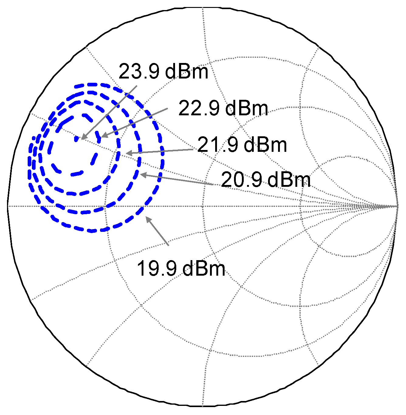
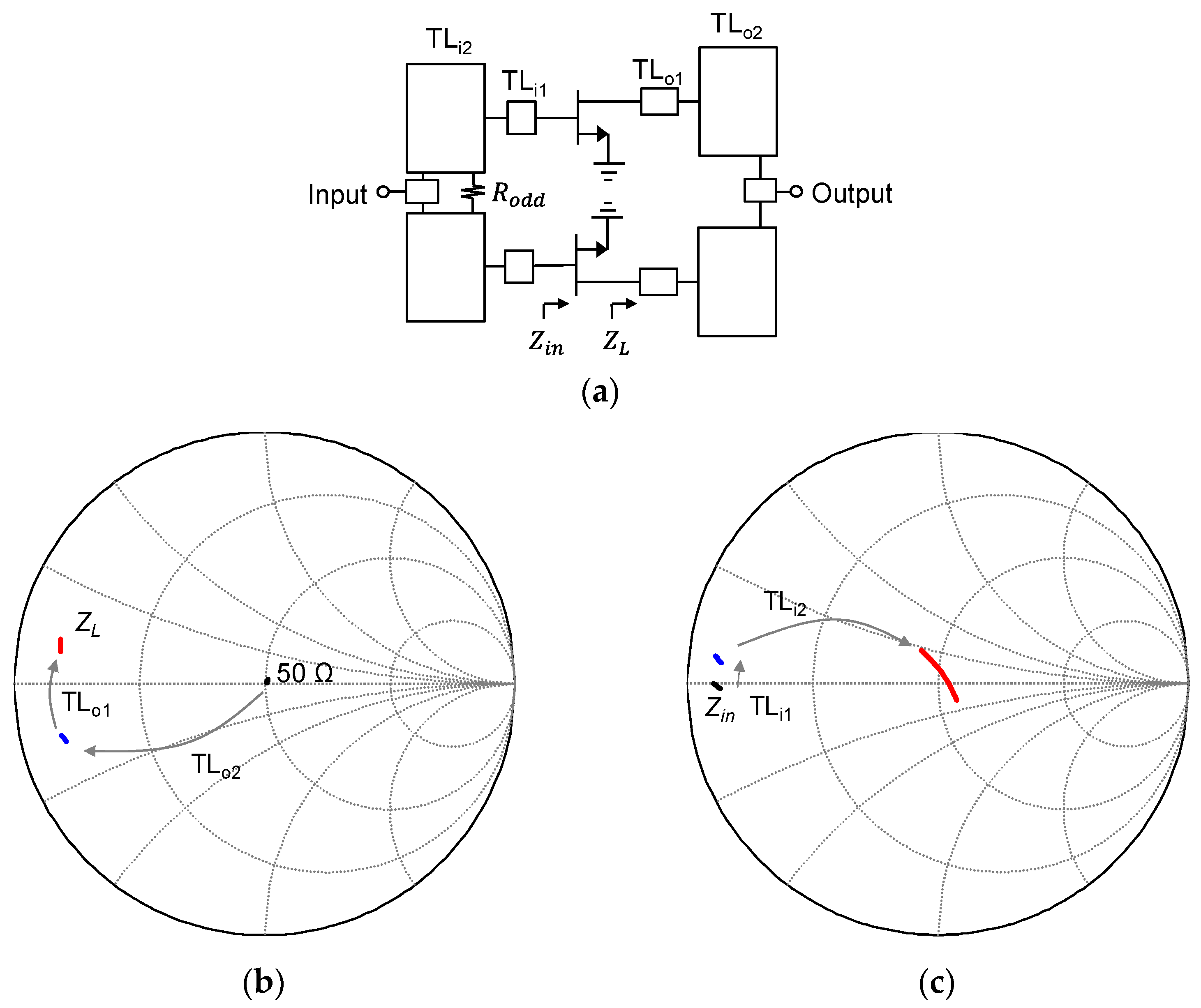
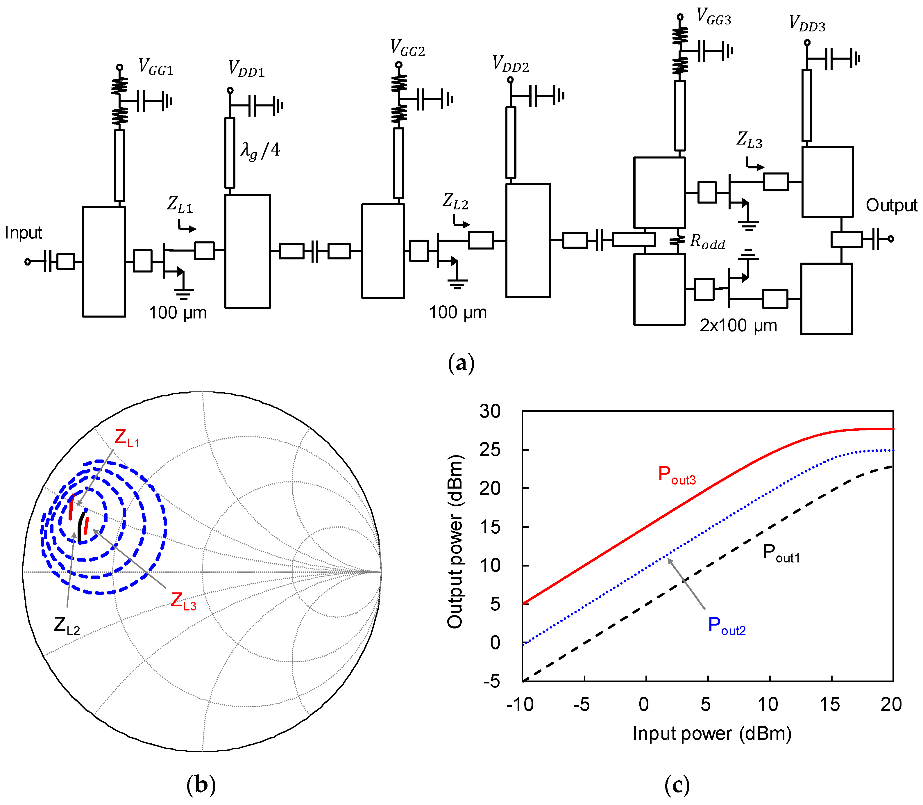
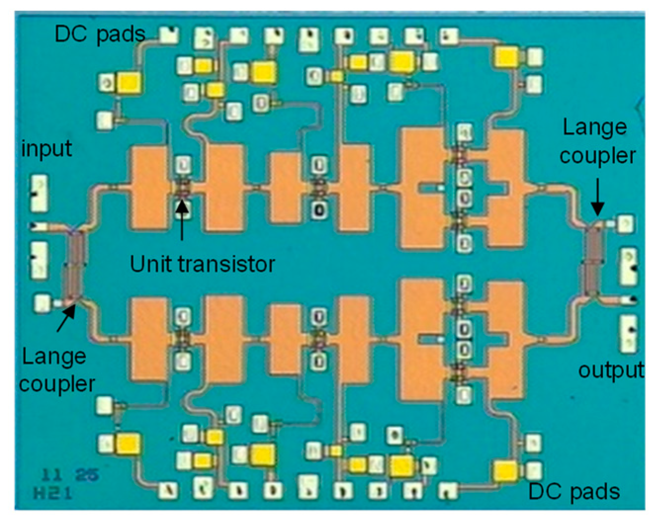
2.2. Design of W-Band Three-Stage Power Amplifier

The HEMT with a 100-μm gate width (four fingers) was selected as a unit transistor for the power amplifier design. It was biased to flow the current ( I DD ) of 45.6 mA at a drain bias voltage ( V DD ) of 10 V. Its optimum load and source impedances were obtained from the load-pull simulation as Z L , opt = 8.2 + j 12.0 Ω, Z S , opt = 5.5 + j 0.7 Ω, respectively, at a center frequency ( f 0 ) of 90 GHz, as illustrated in Figure 1. On this condition, the common-source transistor can deliver an output power of 24.8 dBm with a gain of 3.2 dB at 3-dB gain compression point. Two unit transistors were combined in the final stage for higher output power, which theoretically lowers the input and output impedances by half.
The impedance matching network can be designed using the tapered lines with continuously varying impedance and using the lines with stepped impedances [14]. In this work, the stepped impedance transformation was adopted for the compact design using microstrip lines which are fabricated on a 100 μm-thick high-resistivity Si substrate (loss tangent = 0.015). Note that SiC substrates exhibit a few orders of magnitude higher resistivity than Si one [8,15]. Figure 2 shows the simulated characteristics of the microstrip lines as a function of signal metal width at 90 GHz. As expected, characteristic impedance lowers and guide wavelength shortens as the signal width increases. Therefore, the impedance matching networks consisting of low- Z 0 lines can result in the small physical length. As shown in Figure 2b, the dielectric loss exceeds the conductor loss for the width ≥ 20 μm and remains almost constant. The conductor loss continuously reduces as the width increases. As a result, the low- Z 0 lines with wide metal width ensures lower total loss. Based on this simulation result, the low- Z 0 lines are adopted in this work for the design of low-loss impedance matching networks.
Figure 3a shows the schematic of the final stage, consisting of two 100 μm-wide HEMTs and low- Z 0 lines that were used for the impedance transformation. At the output side, a 50 Ω termination was transformed to low impedance by TLo2 with Z 0 of 28 Ω and moved to the optimum load impedance ( Z L , opt ) by a short TLo1 with a relatively high Z 0 of 62 Ω, as illustrated in Figure 3b. The input was matched to a 50 Ω by using low- Z 0 TLi2 ( Z 0 = 26 Ω) and short TLi1 ( Z 0 = 60 Ω), as demonstrated in Figure 3c. The widths of TLi1 and TLo1 lines were determined by considering those of the gate and drain pads of the HEMT.
In order to achieve enough gain at W-band, two drive stages are added in front of the final stage as shown in Figure 4a. The first and second stages consist of the unit transistors (100 μm-wide HEMT), so that the gate width ratio between stages is 1:1:2. Inter-stage and input matching networks are designed using low-impedance lines (around 20 Ω) as like output matching network. Considering the limited gain of the transistor at f 0 , the load of each transistor (ZL1, ZL2, and ZL3) is matched to the optimum load impedance for each stage to produce high power and fully drive the next stage, as shown in Figure 4b. It is confirmed by Figure 4c that each stage provides almost equal gain around 5.0 dB at low input power, where Pout1, Pout2, and Pout3 are the powers produced by each stage at the drain. This figure also indicates that the final stage is the first to saturate and produces nearly 3-dB higher power than 2nd stage as expected from the gate width ratio. These results confirm that each stage is properly designed to have enough power gain and output power.
Gate and drain bias circuits are designed using the quarter-wave long ( λ g / 4 ) lines with shunt capacitors which are attached to the low- Z 0 lines used for impedance matching, as depicted in Figure 4a. The low-frequency stabilities improved by introducing resistors and capacitors in the gate bias lines. In order to suppress the odd-mode oscillations, the resistor Rodd was inserted between two gate terminals of the final stages.
To double the output power, two of the three-stage power amplifier in Figure 4a were combined using Lange couplers as shown in Figure 5a. The width, spacing, and length of the coupled lines in the Lange coupler were optimized to have an equal power division with a minimum loss and 90° phase difference between two output ports, which is essential to achieve high combining efficiency and good input/output return losses [16]. The isolation was also considered in the design of the Lange coupler to minimize the coupling between two amplifiers, which improves the stability of the entire amplifier [17]. The designed final amplifier exhibits the simulated gain of 14.4 dB with good input and output return loss as shown in Figure 5b. The saturated output power was simulated to be 29.4 dBm with a PAE of 15.4% at 90 GHz as in Figure 5c. There are many low-impedance microstrip lines with very wide signal widths in the designed power amplifier, generating the discontinuities between other components such as narrow-width lines or DC-blocking capacitors. Therefore, a 2.5-dimensional electromagnetic (EM) simulation was carried out using a commercial simulation tool (Momentum in the Keysight Advanced Design System) to optimize the dimensions of the microstrip lines.

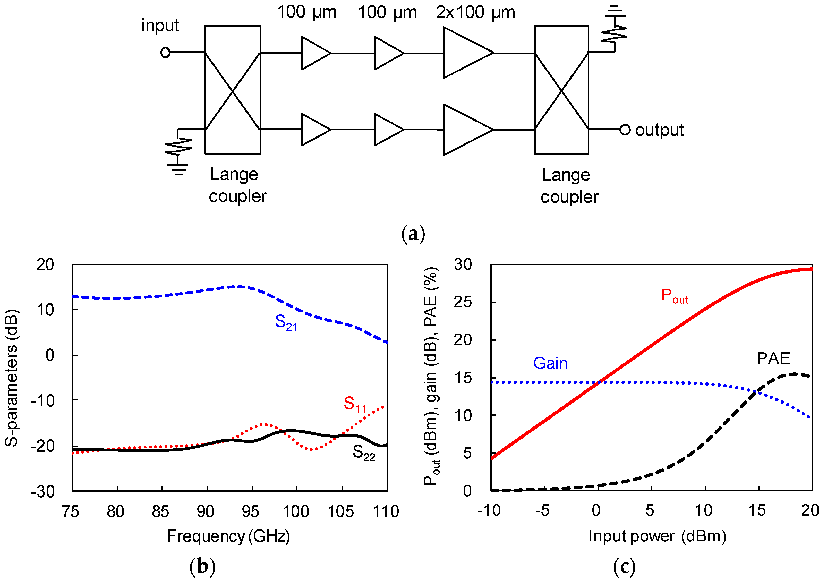
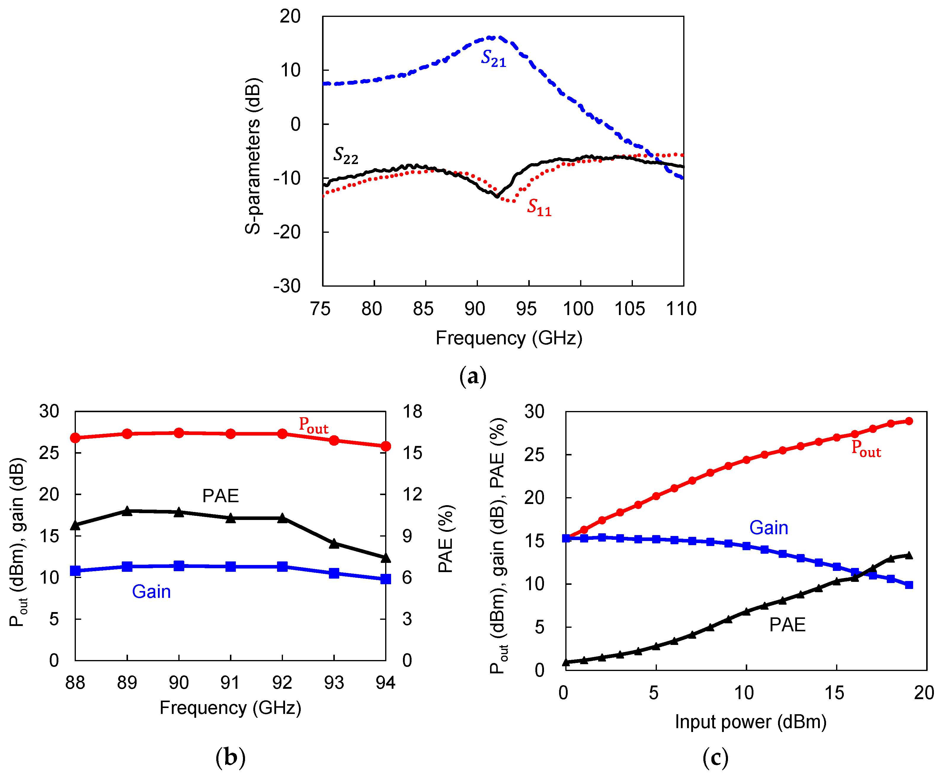
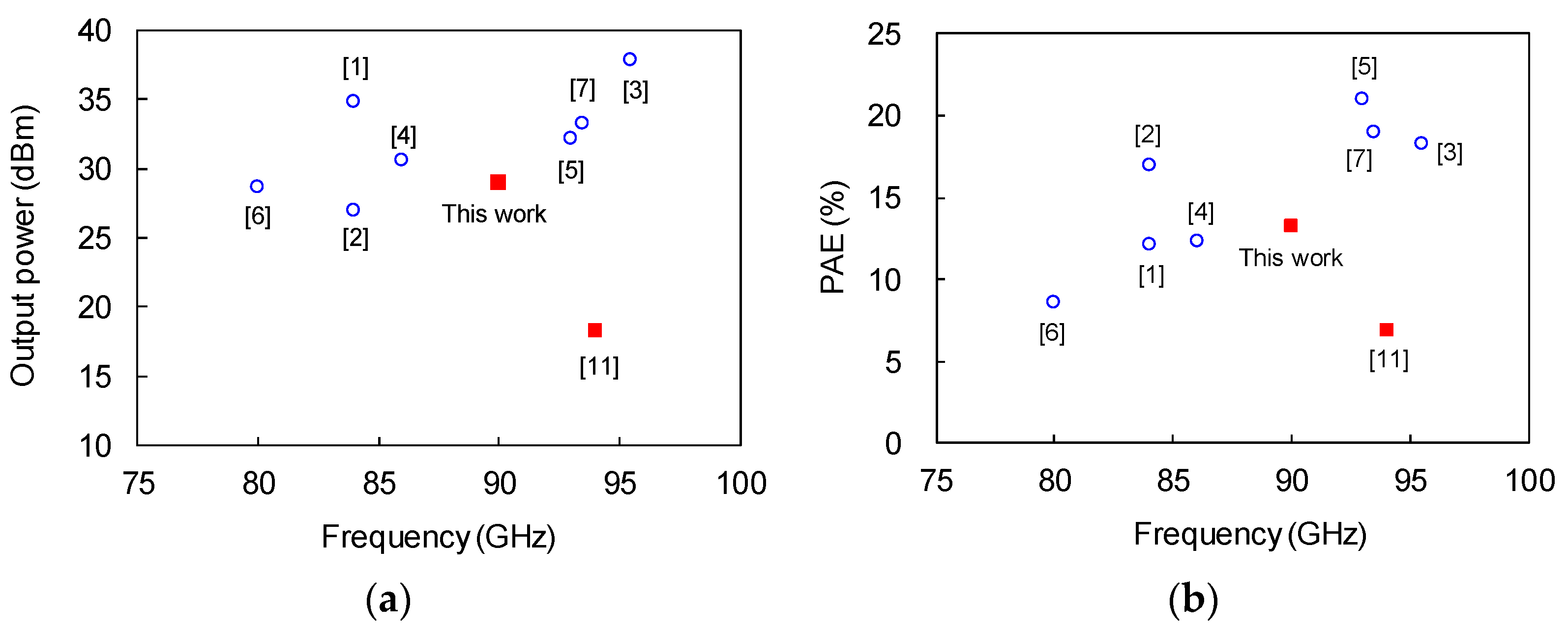
3. Measurement Results

Figure 6 is a graphic representation of the fabricated W-band power amplifier in a 60 nm GaN-on-Si HEMT foundry. Overall chip size is 2.4 mm × 2.0 mm including DC and RF pads. The chip was mounted on the gold-plated copper block by eutetic bonding for a good heat sink. The small- and large-signal performances were measured by on-wafer probing at the drain bias voltage V DD of 10 V. The measured S-parameters are given in Figure 7a. The maximum gain ( S 21 ) of 16.1 dB is achieved at 92.2 GHz with a 3-dB bandwidth of 6.3 GHz from 87.8 to 94.1 GHz, where S 11 and S 22 are better than −8.9 and −9.5 dB, respectively.
The power measurement was performed in the continuous-wave condition. Figure 7b shows the measured output power (Pout), gain, and PAE with frequency. The input power is fixed at 16.0 dBm in this measurement. The measured Pout is higher than 26.5 dBm with gain > 10.5 dB and PAE > 8.5% from 88 to 93 GHz. Figure 7c shows the measured power performance with the input power at 90 GHz. The peak power is as high as 28.9 dBm at an input power of 19.0 dBm, corresponding to the power density of 1.94 W/mm. The peak PAE was measured to be 13.3%. Figure 8 shows the performance comparison between the reported W-band GaN-on-SiC and GaN-on-Si power amplifier ICs. To the best of the authors’ knowledge, the power amplifier IC in this work presents the highest output power and power density performance among the reported GaN-on-Si power amplifier ICs operating at a W-band. It is also worthwhile to note that its output power and PAE performances are comparable to those of GaN-on-SiC power amplifier ICs, even though they are worse, as demonstrated in Figure 8.

4. Conclusions

In this work, the W-band three-stage power amplifier IC was presented using the commercially available GaN-on-Si HEMT foundry. The low impedance lines were utilized in the impedance matching networks to reduce the microstrip losses and thus improve the output power and efficiency. The load of each stage was matched to the optimum impedance to produce enough output power to drive the next stage. In the measurement, the GaN-on-Si power amplifier IC showed the high output power of 28.9 dBm with high power density (1.94 W/mm) and PAE (13.3%) at W-band, which are comparable to the GaN-on-SiC counterpart. This work demonstrates that the GaN-on-Si HEMT technologies can be potentially applied to low-cost solutions for W-band high-power commercial applications.
There is still a need to improve the performance of GaN-on-Si power amplifiers, especially output power per chip. For this purpose, further research will be carried out to combine the larger number of unit transistors using the efficient on-chip power combiners. The thermal design is also required to reduce the performance degradation by the heat generated by the transistors. In addition, the research should be conducted to develop the high-quality epitaxial growth of the GaN channel on the silicon, allowing for similar performance of the GaN-on-SiC transistor.

Author Contributions

Conceptualization, J.J., S.K. and W.K.; methodology, Y.J. and J.K.; software, Y.J. and J.K.; validation, Y.J.; formal analysis, J.K.; data curation, Y.J. and J.J.; writing—original draft preparation, J.J.; writing—review and editing J.J.; visualization, Y.J.; supervision, J.J., S.K. and W.K.; funding acquisition, J.J., S.K. and W.K. All authors have read and agreed to the published version of the manuscript.

Funding

This work was supported by Agency for Defense Development under the contract UC170028FD.

Conflicts of Interest

The authors declare no conflict of interest.

References

  1. Schellenberg, J.M. A 2-W W-Band GaN traveling-wave amplifier with 25-GHz bandwidth. IEEE Trans. Microw. Theory Tech. 2015, 63, 2833–2840. [Google Scholar] [CrossRef]
  2. Micovic, M.; Kurdoghlian, A.; Moyer, H.P.; Hashimoto, P.; Hu, M.; Antcliffe, M.; Willadsen, P.J.; Wong, W.S.; Bowen, R.; Milosavljevic, I.; et al. GaN MMIC PAs for E-Band (71 GHz–95 GHz) Radio. In Proceedings of the 2008 IEEE Compound Semiconductor Integrated Circuits Symposium, Monterey, CA, USA, 12–15 October 2008; pp. 1–4. [Google Scholar] [CrossRef]
  3. Wang, W.; Guo, F.; Chen, T.; Wang, K. 24.8 A W-band power amplifier with distributed common-source GaN HEMT and 4-Way Wilkinson-Lange combiner achieving 6W output power and 18% PAE at 95GHz. In Proceedings of the 2020 IEEE International Solid-State Circuits Conference (ISSCC), San Francisco, CA, USA, 16–20 February 2020; pp. 376–378. [Google Scholar] [CrossRef]
  4. Niida, Y.; Kamada, Y.; Ohki, T.; Ozaki, S.; Makiyama, K.; Minoura, Y.; Okamoto, N.; Sato, M.; Joshin, K.; Watanabe, K. 3.6 W/mm high power density W-band InAlGaN/GaN HEMT MMIC power amplifier. In Proceedings of the 2016 IEEE Topical Conference on Power Amplifiers for Wireless and Radio Applications (PAWR), Austin, TX, USA, 24–27 February 2016; pp. 24–26. [Google Scholar] [CrossRef]
  5. Shaobing, W.; JianFeng, G.; Weibo, W.; Junyun, Z. W-Band MMIC PA with ultrahigh power density in 100-nm AlGaN/GaN Technology. IEEE Trans. Electron. Devices 2016, 63, 3882–3886. [Google Scholar] [CrossRef]
  6. Cwiklinski, M.; Friesicke, C.; Bruckner, P.; Schwantuschke, D.; Wagner, S.; Lozar, R.; Mabler, H.; Quay, R.; Ambacher, O. Full W-Band GaN Power Amplifier MMICs using a novel type of broadband radial stub. IEEE Trans. Microw. Theory Tech. 2018, 66, 5664–5675. [Google Scholar] [CrossRef]
  7. Micovic, M.; Kurdoghlian, A.; Margomenos, A.; Brown, D.F.; Shinohara, K.; Burnham, S.; Milosavljevic, I.; Bowen, R.; Williams, A.; Hashimoto, P.; et al. 9296 GHz GaN power amplifiers. In Proceedings of the 2012 IEEE/MTT-S International Microwave Symposium Digest, Montreal, QC, Canada, 17–22 June 2012; pp. 1–3. [Google Scholar] [CrossRef]
  8. Quay, R.; Schwantuschke, D.; Ture, E.; Van Raay, F.; Friesicke, C.; Krause, S.; Müller, S.; Breuer, S.; Godejohann, B.; Brückner, P. High-Power Microwave GaN/AlGaN HEMTs and MMICs on SiC and silicon substrates for modern radio communication. Phys. Status Solidi 2018, 215, 1–7. [Google Scholar] [CrossRef]
  9. Gasmi, A.; El Kaamouchi, M.; Poulain, J.; Wroblewski, B.; Lecourt, F.; Dagher, G.; Frijlink, P.; Leblanc, R. 10 W power amplifier and 3W transmit/receive module with 3 dB NF in Ka band using a 100nm GaN/Si process. In Proceedings of the 2017 IEEE Compound Semiconductor Integrated Circuit Symposium (CSICS), Miami, FL, USA, 22–25 October 2017; pp. 1–4. [Google Scholar] [CrossRef]
  10. Moron, J.; Leblanc, R.; Lecourt, F.; Frijlink, P. 12W, 30% PAE, 40 GHz power amplifier MMIC using a commercially available GaN/Si process. In Proceedings of the 2018 IEEE/MTT-S International Microwave Symposium-IMS, Philadelphia, PA, USA, 10–15 June 2020; pp. 1457–1460. [Google Scholar] [CrossRef]
  11. Marti, D.; Lugani, L.; Carlin, J.-F.; Malinverni, M.; Grandjean, N.; Bolognesi, R. W-Band MMIC Amplifiers Based on AlInN/GaN HEMTs Grown on Silicon. IEEE Electron. Device Lett. 2016, 37, 1025–1028. [Google Scholar] [CrossRef]
  12. Colangeli, S.; Ciccognani, W.; Longhi, P.E.; Pace, L.; Poulain, J.; Leblanc, R.; Limiti, E. Linear Characterization and Modeling of GaN-on-Si HEMT Technologies with 100 nm and 60 nm Gate Lengths. Electron 2021, 10, 134. [Google Scholar] [CrossRef]
  13. Cripps, S. RF Power Amplifiers for Wireless Communications, 2nd ed.; Artech House: Norwood, MA, USA, 2006; pp. 92–100. ISBN 9781596930193. [Google Scholar]
  14. Li, J. Wideband PCB-to-Connectors Impedance Adapters for Liquid Crystal-based Low-loss Phase Shifters. In Proceedings of the 2020 50th European Microwave Conference (EuMC), Utrecht, The Netherlands, 12–14 January 2021; pp. 546–549. [Google Scholar]
  15. Timothy, B. GaN-on-Silicon-Present capabilities and future directions. In Proceedings of the AIP Conference, Mayan Riviera, Mexico, 28 August–2 September 2016; Volume 1934, pp. 1–10. [Google Scholar] [CrossRef]
  16. Pozar, D. Microwave Engineering, 4th ed.; John Wiley & Sons, Inc.: Hoboken, NJ, USA, 2011; pp. 343–362. ISBN 0470631554. [Google Scholar]
  17. Choe, W.; Kim, S.; Kim, W.; Jeong, J. W-band mixer with high image rejection by mismatch compensation using buffer amplifier. IEEE Access 2020, 8, 5824–5833. [Google Scholar] [CrossRef]
Figure 1. Load-pull contours for output power of 100 μm-wide HEMT at 90 GHz.
Applsci 11 09017 g001
Figure 2. Simulated characteristics of the microstrip line as a function of signal width at 90 GHz. (a) Characteristic impedance Z 0 and wavelength λ g . (b) Attenuation per a wavelength ( λ g ).
Applsci 11 09017 g002
Figure 3. Design of final stage (two 100 μm-wide HEMTs in parallel). (a) Circuit schematic. Impedance trajectories of (b) output matching and (c) input matching networks from 88 to 92 GHz.
Applsci 11 09017 g003
Figure 4. Design of three-stage power amplifier. (a) Circuit schematic. (b) Load impedance of each stage of designed amplifier (from 88 to 92 GHz) on top of load-pull contours at 90 GHz. (c) Simulated output power of each stage as a function of input power at 90 GHz.
Applsci 11 09017 g004
Figure 5. Design of final three-stage power amplifier using Lange couplers. (a) Circuit schematic. (b) Simulated S-parameters. (c) Simulated output power, gain, and PAE as a function of input power at 90 GHz.
Applsci 11 09017 g005
Figure 6. Fabricated W-band power amplifier IC using 60 nm GaN-on-Si HEMT foundry (chip size: 2.4 mm × 2.0 mm).
Applsci 11 09017 g006
Figure 7. Measurement results. (a) S-parameters. (b) Output power, gain, and PAE versus frequency with input power of 16.0 dBm. (c) Pout, gain, and PAE versus input power at a frequency of 90 GHz.
Applsci 11 09017 g007
Figure 8. Comparison of the reported W-band GaN power amplifier ICs (circles: GaN-on-SiC, squares: GaN-on-Si). (a) Output power versus frequency. (b) PAE versus frequency.
Applsci 11 09017 g008
Publisher’s Note: MDPI stays neutral with regard to jurisdictional claims in published maps and institutional affiliations.

