Article

In Situ X-ray Measurements to Follow the Crystallization of BaTiO3 Thin Films during RF-Magnetron Sputter Deposition

1
Deutsches Elektronen-Synchrotron, Notkestr. 85, 22607 Hamburg, Germany
2
SLAC National Accelerator Laboratory, 2575 Sand Hill Road, Menlo Park, CA 94025, USA
3
European XFEL, Holzkoppel 4, 22869 Schenefeld, Germany
4
Department of Chemistry, Aarhus University, Langelandsgade 140, 8000 Aarhus C, Denmark
5
2nd. Institute of Physics B and JARA-FIT, RWTH Aachen University, Otto-Blumenthal-Str. 1, D-52074 Aachen, Germany
*
Author to whom correspondence should be addressed.
Appl. Sci. 2021, 11(19), 8970; https://doi.org/10.3390/app11198970
Submission received: 27 August 2021 / Revised: 22 September 2021 / Accepted: 23 September 2021 / Published: 26 September 2021
(This article belongs to the Special Issue Recent Advances in Application of Coatings and Films)

Abstract

:
Here, we report on adding an important dimension to the fundamental understanding of the evolution of the thin film micro structure evolution. Thin films have gained broad attention in their applications for electro-optical devices, solar-cell technology, as well storage devices. Deep insights into fundamental functionalities can be realized via studying crystallization microstructure and formation processes of polycrystalline or epitaxial thin films. Besides the fundamental aspects, it is industrially important to minimize cost which intrinsically requires lower energy consumption at increasing performance which requires new approaches to thin film growth in general. Here, we present a state of the art sputtering technique that allows for time-resolved in situ studies of such thin film growth with a special focus on the crystallization via small angle scattering and X-ray diffraction. Focusing on the crystallization of the example material of BaTiO 3 , we demonstrate how a prototypical thin film forms and how detailed all phases of the structural evolution can be identified. The technique is shaped to enable a versatile approach for understanding and ultimately controlling a broad variety of growth processes, and more over it demonstrate how to in situ investigate the influence of single high temperature sputtering parameters on the film quality. It is shown that the whole evolution from nucleation, diffusion adsorption and grain growth to the crystallization can be observed during all stages of thin film growth as well as quantitatively as qualitatively. This can be used to optimize thin-film quality, efficiency and performance.

1. Introduction

The industrial market for thin films requires the production of more efficient layers with better performance, lower energy consumption, and preferably to lower production cost. With an increasing demand of functional thin films the control and influence of the preparation parameters has to be investigated in situ during the thin film production. A key role in a broad spectrum of applications such as electro-optical devices, solar cell technology or storage devices [1,2,3,4] plays the crystallization either for polycrystalline or epitaxial thin films [5,6]. State of the art thin film research has reached a point where only in situ measurements can help optimizing the thin film production, because this way, the influence of the different sputtering parameters can be followed in real time during the deposition process.
To follow the preparation of oxide thin films, we were using the characteristic features of the modern synchrotron radiation source PETRA III [7], a compact and low-weight sputtering unit [8], and the investigation techniques in situ grazing incidence small angle X-ray scattering (GISAXS) and in situ grazing incidence X-ray powder diffraction (GIXRPD) simultaneously, as well as in situ X-ray reflectivity (XRR) measurements [9,10].
In this work, we follow the crystallization process in situ during the high temperature deposition above the crystallization energy. We deposit BaTiO 3 at 600 C and followed the film evolution from early formation to polycrystalline thin film of around 40 nm.

2. Materials and Methods

In the present work, BaTiO 3 thin film evolution was studied at P03 at PETRA III [11], two 2D detectors were used simultaneously. One 2D detector (Pilatus 1M, 981 × 1043 pixels, pixel size of 172 μ m × 172 μ m) was used for GISAXS at a Sample-to-Detector Distance of SDD = 4 m. The X-ray beam had an energy of 13 keV and a beam size of 40 μ m (horizontal) × 20 μ m (vertical) FWHM, and the angle of incidence ( α i ) was set to 0.5 . This angle is above the critical angle of the materials involved. A second single-photon counting pixel detector with 487 × 619 pixel of 172 μ m each (Pilatus 300k, Dectris, Baden, Switzerland) was mounted on the detector arm of the diffractometer with SDD = 0.28 m covering the Q-range from 2 Å−1–4.5 Å−1. With this second 2D detector, we were following the evolution by GIXRPD simultaneously to the GISAXS measurement. Both detectors were in air. The measurements were performed with the following parameters. The plasma process and substrate heating was started 10 min. before opening the shutter in front of the sputtering target. The sputtering power on the BaTiO 3 target was 14 W/cm2 and the gas mixture was 80% Argon (Ar) and 20% Oxygen (O 2 ) with a total flow of 1 standard cubic centimetre per minute (SCCM), and a substrate temperature of 600 C. The distance between the sputtering target and substrate was fixed at a distance of 4 cm. The films were deposited on pre-cleaned SiO 2 wafers with a size of 10 × 10 mm 2 . A more detailed description of the measurement can be found here [8,10]. SiO 2 wafers are not the industrial standard for BaTiO 3 thin film deposition, but we have chosen it to avoid surface related influence on the crystallization process. A more detailed study of the influence of various parameters, such as surface structure and deposition temperature, on the crystallization behavior will be published elsewhere. 
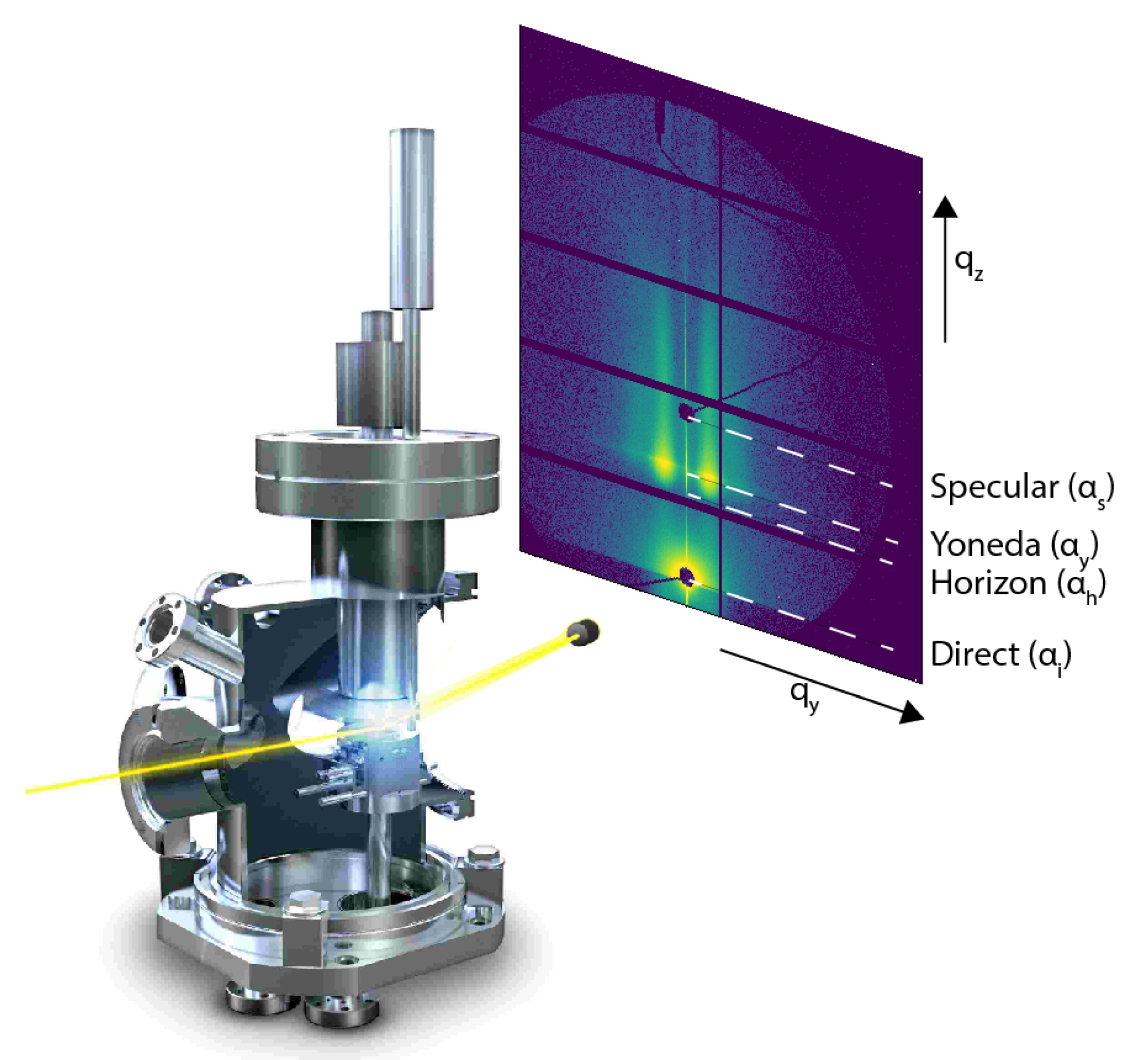
Figure 1 illustrates the principal scheme of the experiment. The X-rays arrived from the left hand side and hit the wafer inside the sputtering unit under gracing incidence and get detected with the 2D detector behind the chamber.

3. Results and Discussion

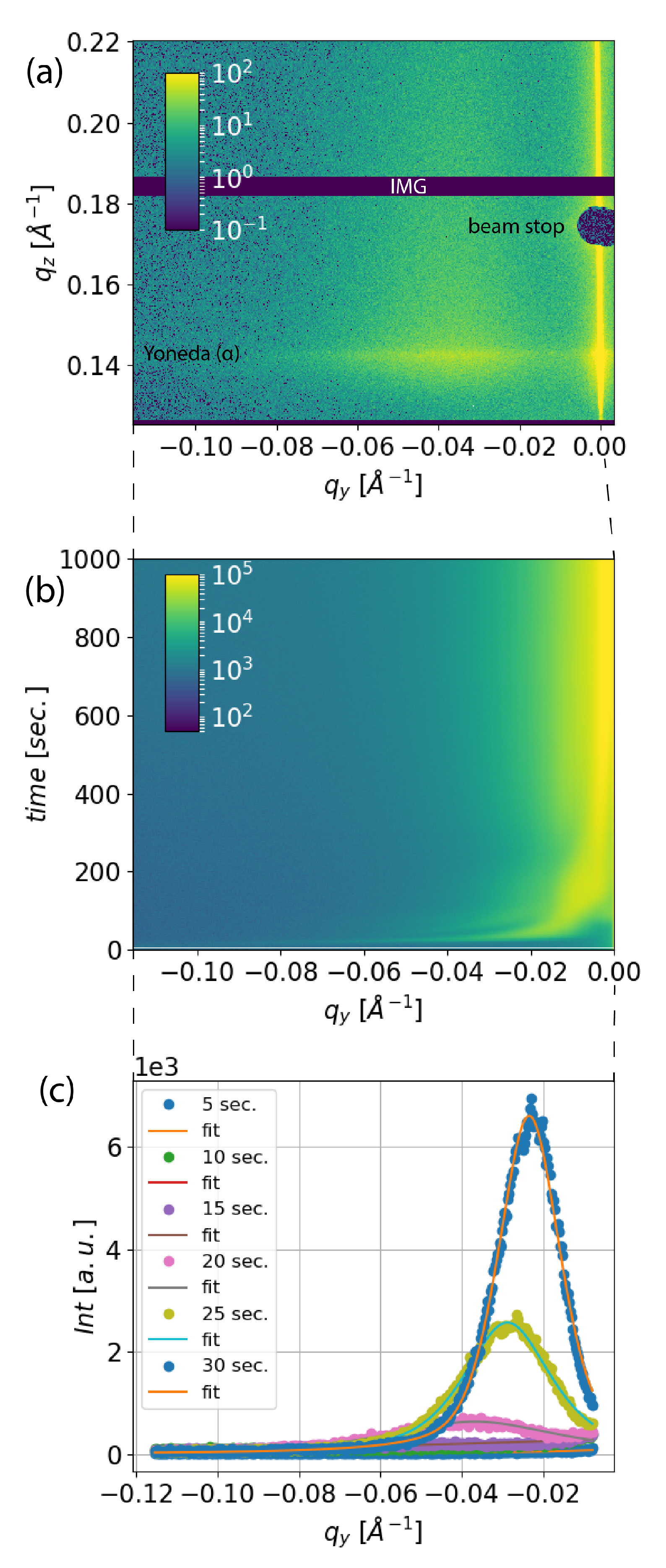
This in situ experiment recorded the film evolution continuously in reciprocal space, without interrupting the sputtering process. Exemplary patterns for the GISAXS detector can be seen in Figure 1. To analyze these patterns in more detail, horizontal cuts were taken at the level of the Yoneda peak [12]. The Yoneda peak occurs when the exit angle of the scattered beam is close to the critical angle due to signal enhancement from the Vineyard effect [13]. This results in a bright band of intensity at the critical angle ( α c ). Below the critical angle the scattering intensity decreases quadratically to zero. With the refraction index n = 1 δ + i β including the real part δ and the imaginary part i β , it depends strongly on the wavelength λ and the electron density. Therefore, it is a material dependent effect when the wavelength is constant.
These patterns (seen in Figure 1 and Figure 2a) show a clear evolution perpendicular to the Yoneda peak over the deposition time. This relates to density correlations and arise from a the structure factor with characteristic modulations parallel to the surface. The peaks were fitted with a pseudo-Voigt function (see Figure 2) p V ( x ) = η G ( x ) + ( 1 η ) L ( x ) , with G(x) the sum of a Gaussian peak and L(x) the Lorentzian peak, as well as the mixing parameter η which describes the fraction of each function.
It shows that the particle distance initially appears at higher q y and shifts towards smaller q over deposition time. This shift indicates a coalescence, i.e., mainly a fusion phenomenon of adjacent nuclei or clusters, which leads to an increase of the average center-to-center distance. From the fit, we can take the FWHM, amplitude and position. The latter depicts the center-to-center distance, as mentioned before. The amplitude indicates the amount of scattering sources. The peak width is related to the distribution and displays the disorder of cluster and particle arrangement. Therefore, the FWHM is also a strong indicator which indicates a transition from fast increasing ordering to a slower growth of a two-dimensional (2D) cluster arrangement. This means a conversion from a diffusion-mediated coalescence regime to an adsorption-driven cluster growth regime. This expansion persists until one cluster grows radially into another one by the movement of grain boundaries and not by coalescence anymore (shown in Figure 3a–c). This means the surface is covered and the newly arriving particles contribute only in the vertical growth. This describes the early formation (nucleation, diffusion, adsorption and grain growth) for thin films as known from literature [5,6,10]. The relation D 2 π / q enables us to track the mean cluster distance during the growth as a quantitative parameter. The peak broadening in Figure 3a at around 120 s corresponds to the growing additional scattering source of crystalline BaTiO 3 particles until the crystalline particles with δ = 5.8 g/cm 2 have taken over the whole layer.
From the development of the Yoneda peak itself, we were able to get further information about the growth dynamics. Therefore, we have taken cuts in the q y -direction at the position of the Yoneda peak (see Figure 3c). The temporal evolution of the intensity at the Yoneda peak corresponds to the surface coverage or particle density at the surface, which leads to a change in the scattering distribution. At the beginning of the deposition, a clear Yoneda peak of S i O 2 can be seen. At a deposition time of 20 s, the Yoneda peak of amorphous BaTiO 3 , with a δ = 2.9 g/cm 2 , appears and after a deposition time of 60 s, another Yoneda peak appears. This is a relatively broad peak that shows up at δ = 5.8 g/cm 2 which correspond to polycrystalline BaTiO 3 . As mentioned above, the Yoneda peak depends on the material—on the electron density, to be precise, which changes when the crystallization launches. This is were it shows an alteration around 30 s after the start of the deposition. It starts with a broadening of the Yoneda wing in q z , leads to a second line at the density of polycrystalline BaTiO 3 , and ends with a disappearing line at the density of the amorphous clusters. These density findings accord with the literature values for BaTiO 3 [14,15].
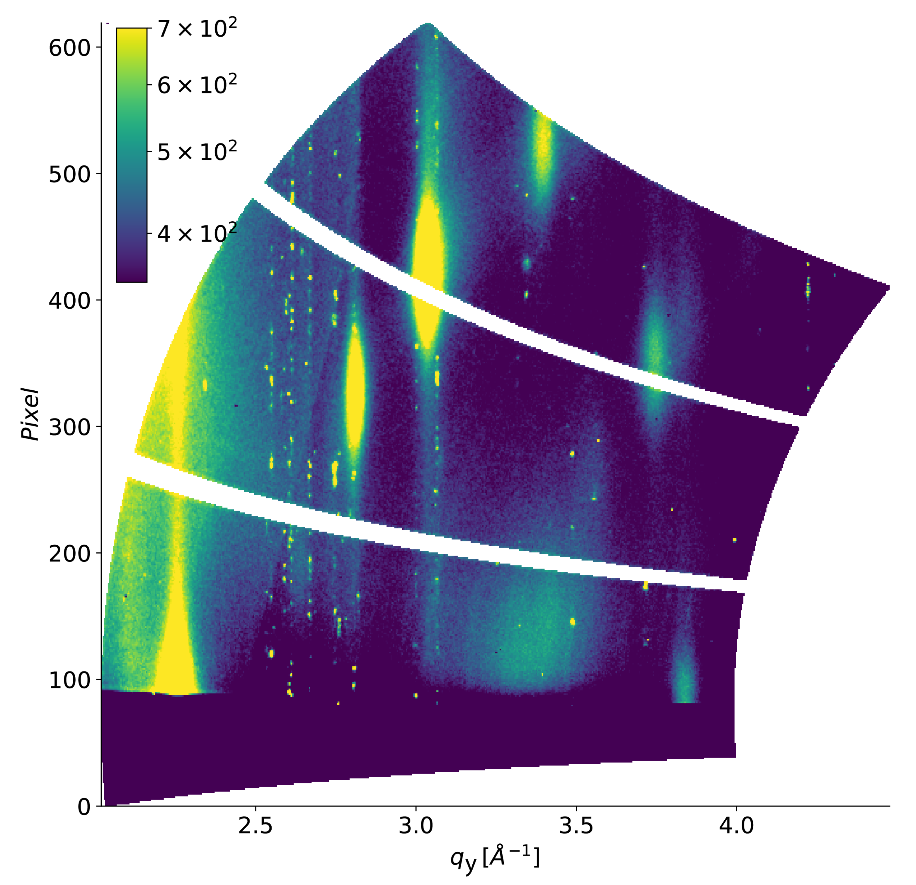
During this experiment, we collected the wide angle scattering (WAX) with a second detector simultaneously. An exemplary pattern taken after 500 s of deposition is shown in Figure 4, it shows a detector tilt and rotation corrected pattern which was azimuthal resorted using the Python package pyFAI [16]. The software was calibrated by performing a measuring with a NIST standard.
The peak positions for cubic BaTiO 3 are marked and show a good agreement. Small offsets at the higher angle peaks are shown and can be explained as finite-size effect and temperature introduced stress on the wafer and the thin film. The peak broadening of the [200]-peak and the double peak structure at the [211]-peak can be explained with the occurrence of tetragonal BaTiO 3 . The preferred orientation arises from particles being oriented on the surface and enhancing the intensities of more defined Bragg reflections, while reducing the intensities of others. [18] The preferred orientation is diminishing with increasing film thickness as shown in Figure 5. This can be explained with the fast increasing film thickness, a layer-plus-island growth and the therefore decreasing influence of the surface and relaxation process due to misfit dislocations [5,6], but still can be seen until the end of deposition. Figure 6 shows the peak evolution by plotting the azimuthal resorted patterns versus time during the deposition at 600 C and selected GIXRPD pattern after 100, 500 and 1000 s. Figure 7 shows exemplary pseudo-Voigt fits of the peaks. The increasing amplitude corresponds to the quantity of diffraction sources, i.e., crystallites, and the peak width correspond to the nano-crystalline size. The azimuthal integrated patterns versus time can be fitted with a pseudo-Voigt function to extract the peak width and amplitude. Figure 6 shows the results of five second binned fits over time for the [110] and [200] peak, these peak positions are in good agreement with literature [17,19]. The [200] peak occurs after about 200 s of deposition and the [110] peak after about 250 s. This is about 140 s after the appearance of the crystalline Yoneda peak. In the early crystallization stage, the amount of diffraction sources are to small too overcome the background and noise in the GIXRPD detector. With the simultaneous use of two detectors for GISAXS and GIXRPD we have followed the crystallization in detail through the whole evolution of the thin film growth. First, it appears after around 60 s in cuts along q z at the Yoneda peak (see Figure 3c) as slowly growing peak at the density of crystalline BaTiO 3 . After a growing amount of scattering sources through the film thickness it leads to a broadening of the peak along q y direction (see Figure 2b and Figure 3a) at around 100 s. And finally it appears as a scattering signal in the GIXRPD detector (see Figure 5 and Figure 6) after around 200 s.
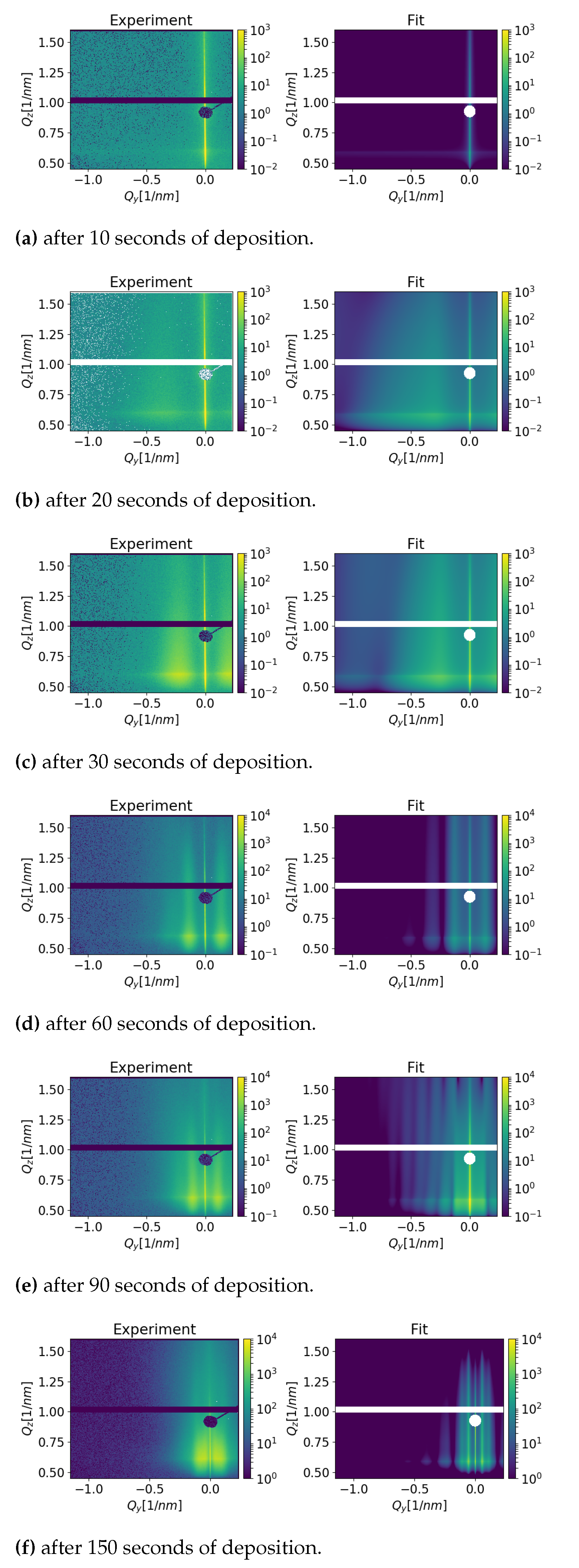
To confirm and refine these findings, we used the software BornAgain (BA) [20] to simulate and fit the evolution of the thin film. For the early formation, we get the best results for small sized hemispherical shaped particle ( δ = 2.9 g/cm 2 ) with a small distribution on the height of 3 nm and the radius of 3 nm for the beginning and growing over time. In the early stage, there is only a cumulative disorder of inter-particle distances along the X-ray footprint. This corresponds to the early stage of nucleation, diffusion and adsorption (see Figure 7a–c). Over time, the mean particle diameter rises, forming small clusters growing in diameter and shrinking in distance. At this stage, the best model assumes uniform hemispherical clusters of radius R arranged in a 2D hexagonal lattice with the correlation distance D between the lattice points. Assuming that all BaTiO 3 deposited on this triangular area is separated into three individual uniform clusters (see Figure 3d), this leads to the equation:
R = 2 π f A t 3 1 4
With R the micro-domain size, f A the form factor ratio A c i r c l e A h e x a g o n , with A c i r c l e = 3 π R 2 and A h e x a g o n = 3 3 2 t 2 , where t is the side length of the hexagon, with the local maximum for close packing at t = 2 r . This maximum emphasizes the fully covered surface as mentioned before (see Figure 3a).
Since we were depositing on a substrate temperature higher than the known crystallization energy for BaTiO 3 [1,2], a re-crystallization was expected to happen, and was shown in the cuts along the q y direction at about 60 s. Following our evolution modeling, we have assumed a covered surface of hemispherical clusters ( δ = 2.9 g/cm 2 ) with embedded particles ( δ = 5.8 g/cm 2 ). For these particles with the density of crystalline BaTiO 3 , the best fitting shape are cylinders with a radius of 2 nm and a height of 3 nm which grow over time (see Figure 7d). The fitting model with the highest agreement show these cylinders growing near the interface of the substrate to the thin film. After about 100 s of deposition, the best fitting model is a 10nm thick amorphous thin film with a high surface roughness and growing hemispherical ploy-crystalline clusters (see Figure 7f). After the crystallization of the whole thin film the arriving amorphous particle coming from the sputtering target will quickly crystallize. The high surface roughness stays until the end of the deposition which is also confirmed by the missing interference pattern in the q z -cuts at the q = 0 position shown in Figure 3c, which is in strong agreement with the literature [10]. A schematic of the thin film evolution during the deposition is shown in Figure 8.

4. Summary and Outlook

By means of various X-ray diffraction and scattering experiments, we have shown that the characterization of the film formation and film growth, and especially to follow the crystallization, is feasible in real time, thus adding the important dimension to the fundamental understanding of the evolution of the film micro structure. Furthermore, these techniques were used to study the crystallization dependence of the deposition process and the growth on SiO 2 substrate material. It is observed that the whole evolution from nucleation, diffusion adsorption and grain growth to the crystallization can be observed during all stages of thin film growth as well as quantitatively as qualitatively using the prototypical showcase of BaTiO 3 . Investigations of various parameters of the deposition process and their influence on the crystallization such as surface structure and deposition temperature was also performed and will be published elsewhere. A logical next step would be a in situ study of the deposition and crystallization using the thin film pair distribution function analysis (tfPDF) [21].

Author Contributions

P.W. has conceived the experiment. The experiment was performed by P.W., M.I., J.R., W.O., C.B.Z. and U.K. The data was analyzed by P.W. The original draft was written by P.W. with dedicated contributions by M.I. and U.K. All authors have read and agreed to the published version of the manuscript.

Funding

SLAC National Accelerator Laboratory, is supported by the U.S. Department of Energy, Office of Science, Office of Basic Energy Sciences under Contract No. DE-AC02-76SF00515. We acknowledge DESY (Hamburg, Germany), a member of the Helmholtz Association HGF, for the provision of experimental facilities. Parts of this research were carried out at P03 at PETRA III. M.I. acknowledges funding from the Volkswagen Foundation within a Peter Paul Ewald-Fellowship.

Data Availability Statement

Raw data were generated at PETRA III at DESY, Hamburg, large scale facility. Derived data supporting the findings of this study are available from the corresponding author upon reasonable request.

Acknowledgments

The authors gratefully acknowledge K. Pflaum, J. Blume, L. Wilke, M. Fleck and H. Zink and the FS-EC group. Because of their work and efforts the sputtering unit is operational. We further thank J. Rubeck, F. Bertram, R. Doehrmann, K. Schlage, S. Roth, M. Schwartzkopf, P. Pandit, M. Roelsgaard, A-C. Dippel, O. Seeck, L. Song and U. Ruett from the FS-PE group and the Aarhus University for fruitful discussions and help during the beam time at P03. For help in creating the graphic Figure 1. we are indebted to J. Frerichs.

Conflicts of Interest

The authors declare no conflict of interest. The funders had no role in the design of the study; in the collection, analyses, or interpretation of data; in the writing of the manuscript, or in the decision to publish the results.

References

  1. Gonzalo, J.A.; Jimenez, B. Ferroelectricity; WILEY VCH Verlag: Weinheim, Germany, 2005. [Google Scholar]
  2. Lines, M.E.; Glass, A.M. Principles and Application of Ferroelectrics and Related Materials; Oxford University Press Inc.: New York, NY, USA, 2001. [Google Scholar]
  3. Araujo, C.P.D.; Scott, J.F.; Taylor, G.W. Ferroelectric thin Films: Synthesis and Basic Properties; Gordon and Breach Publishers: Amsterdam, The Netherlands, 1996. [Google Scholar]
  4. Rödel, J.; Jo, W.; Seifert, K.T.P.; Anton, E.M.; Granzow, T.; Damjanovic, D. Perspective on the development of lead-free piezoceramics. J. Am. Ceram. Soc. 2009, 92, 1153–1177. [Google Scholar] [CrossRef]
  5. Reichelt, K. Nucleation and growth of thin films. Vacuum 1988, 38, 1083–1099. [Google Scholar] [CrossRef]
  6. Ohring, M. The materials science of thin films. In Vacuum, 2nd ed.; Academic Press: San Diego, CA, USA, 1995; Volume 46. [Google Scholar] [CrossRef]
  7. Franz, H.; Leupold, O.; Röhlsberger, R.; Roth, S.; Seeck, O.; Spengler, J.; Strempfer, J.; Tischer, M.; Viefhaus, J.; Weckert, E.; et al. Technical Report: PETRA III: DESY’s New High Brilliance Third Generation Synchrotron Radiation Source. Synchrotron Radiat. News 2006, 19, 25–29. [Google Scholar] [CrossRef]
  8. Walter, P.; Dippel, A.C.; Pflaum, K.; Wernecke, J.; van den Hurk, J.; Blume, J.; Klemradt, U. A compact and low-weight sputtering unit for in situ investigations of thin film growth at synchrotron radiation beamlines. Rev. Sci. Instrum. 2015, 86, 053906. [Google Scholar] [CrossRef] [PubMed]
  9. Als-Nielsen, J.; McMorrow, D. Elements of Modern X-ray Physics; John Wiley and Sons, Ltd.: New Yourk, NY, USA, 2011. [Google Scholar] [CrossRef] [Green Version]
  10. Walter, P.; Wernecke, J.; Scholz, M.; Reuther, D.; Rothkirch, A.; Haas, D.; Blume, J.; Resta, A.; Vlad, A.; Faley, O.; et al. In situ X-ray measurements over large Q-space to study the evolution of oxide thin films prepared by RF sputter deposition. J. Mater. Sci. 2021, 56, 290–304. [Google Scholar] [CrossRef]
  11. Buffet, A.; Rothkirch, A.; Döhrmann, R.; Körstgens, V.; Abul Kashem, M.M.; Perlich, J.; Herzog, G.; Schwartzkopf, M.; Gehrke, R.; Müller-Buschbaum, P.; et al. P03, the microfocus and nanofocus X-ray scattering (MiNaXS) beamline of the PETRA III storage ring: The microfocus endstation. J. Synchrotron Radiat. 2012, 19, 647–653. [Google Scholar] [CrossRef] [Green Version]
  12. Yoneda, Y. Anomalous surface reflection of X rays. Phys. Rev. 1963, 131, 2010–2013. [Google Scholar] [CrossRef]
  13. Vineyard, G.H. Grazing-incidence diffraction and the distorted-wave approximation for the study of surfaces. Phys. Rev. B 1982, 26, 4146–4159. [Google Scholar] [CrossRef]
  14. Zeng, J.L.; Teng, H.P.; Lu, F.H. Electrochemical deposition of barium titanate thin films on TiN/Si substrates. Surf. Coat. Technol. 2012, 10–13. [Google Scholar] [CrossRef]
  15. Salama, C.A.T.; Siciunas, E. Characteristics of rf Sputtered Barium Titanate Films on Silicon. J. Vac. Sci. Technol. 2002, 9, 91–96. [Google Scholar] [CrossRef]
  16. Kieffer, J.; Karkoulis, D. PyFAI, a versatile library for azimuthal regrouping. J. Phys. Conf. Ser. 2013, 425, 8–13. [Google Scholar] [CrossRef]
  17. Pratt, I. Characteristics of RF sputtered barium titanate thin films. Proc. IEEE 1971, 59, 1440–1447. [Google Scholar] [CrossRef]
  18. Wenk, H.R.; Van Houtte, P. Texture and anisotropy. Rep. Prog. Phys. 2004, 67, 1367–1428. [Google Scholar] [CrossRef]
  19. Pratt, I.H.; Firestone, S. Fabrication of rf-Sputtered Barium Titanate Thin Films. J. Vac. Sci. Technol. 1971, 8, 256. [Google Scholar] [CrossRef]
  20. Burle, J.; Fisher, J.M.; Ganeva, M.; Pospelov, G.; Van Herck, W.; Wuttke, J. BornAgain: Simulate and Fit Grazing Incidence Small-Angle Scattering; 2015. [Google Scholar]
  21. Jensen, K.M.; Blichfeld, A.B.; Bauers, S.R.; Wood, S.R.; Dooryhee, E.; Johnson, D.C.; Iversen, B.B.; Billinge, S. Demonstration of thin film pair distribution function analysis (tfPDF) for the study of local structure in amorphous and crystalline thin films. IUCrJ 2015, 2, 481–489. [Google Scholar] [CrossRef] [PubMed]
Figure 1. Schematic setup for in situ sputter deposition measurements, with the X-ray beam (yellow), the chamber (silver) including the sample holder in grazing incidence geometry and a 2D detector (blue). Shown is a GISAXS pattern after 40 s of deposition of BaTiO 3 at 600 C. Denoted is the specular beam α s = 2 × α i , the Yoneda peak α y = α c + α i with the α c the critical angle, sample horizon α h = α i and the direct beam α d . Not shown is the second GIXRPD Detector.
Applsci 11 08970 g001
Figure 2. Exemplary region of the GISAXS detector of the two dimensional GISAXS patterns taken at the surface diffraction beam line P03 at PETRA III (a). The bottom line starts at the sample horizon and denoted are the beamstop, the Yoneda level, the inter-modular detector gaps (IDG, black stripe). The intensity evolution of the horizontal cuts at the level of the Yoneda peak (b). And the Pseudo-Voigt fits of the Yoneda-cuts during the deposition at 600 C (c). The data points displaying the background subtracted data and the lines the corresponding fit.
Applsci 11 08970 g002
Figure 3. (a) is showing the intensity evolution of at the Yoneda level and (b) the results from the Pseudo-Voigt Fits, given the peak width sigma (S) and the center position (C) as well as the cluster size (CS) for the first 90 s. (c) shows the q z -cuts at the q = 0 position. (d) shows the cluster grow model for the for the first 60 s. Showing 3 nm sized hemispherical shaped particles arranged in a 2D hexagonal lattice.
Applsci 11 08970 g003
Figure 4. Exemplary two-dimensional GIXRPD false color plot showing a tilt, rotation and azimuthal resorted single patterns of GIXRPD of BaTiO 3 after 1000 s of deposition at 600 C. White markers show diffraction lines for bulk cubic BaTiO 3 [17]. The offset is an effect of temperature and finite-size effects. The powder diffraction rings show a clear indication for preferred orientation and also double peak structures and peak broadening where the lattice parameter a = b ≠ c, are indicating tetragonal BaTiO 3 structure. The high-intensity small peaks are background coming from the AlO 2 sample holder and the black part on the bottom is the sample surface. Also shown in the top right corner is the original shape of the 2D detector.
Applsci 11 08970 g004
Figure 5. GIXRPD false color plot showing a tilt and rotation corrected and azimuthal resorted integration versus time in one-second steps on the left hand side. The selected Q-range from 2 Å−1–4 Å−1. On the right hand side exemplary original GIXRPD pattern collected after 100, 500 and 1000 s. The high intensity small peaks are background coming from the AlO 2 sample holder. The early stage of deposition shows a more diffuse scattering at around 2 Å−1 and 3.5 Å−1. This turns into a preferred orientation for the early crystallization which later evolves into a more evenly distributed poly-crystalline ring structure.
Applsci 11 08970 g005
Figure 6. Exemplary fits of the [110] and [200] BaTiO 3 peaks versus time. Showing the evolution of the peak width and amplitude of the peaks during the deposition at 600 C. The GIXRPD patterns were binned for five seconds due to the background and noise. The [200] BaTiO 3 peak at 3.1 Å−1 occurs after about 200 s and the [110] BaTiO 3 peak at 2.2 Å−1 occurs after about 250 s of deposition. The [200] BaTiO 3 peak shows some peak broadening in the early stage indicating the existence of tetragonal BaTiO 3 and with time developing a homogeneous average poly-crystallization size showing by the width comparison to the [110] BaTiO 3 peak. The increasing amplitude corresponds to the quantity of diffraction sources, i.e., crystals. The different intensity in the beginning corresponds to the increasing background.
Applsci 11 08970 g006
Figure 7. GISAXS patterns and fit of BaTiO 3 after the deposition time marked in Figure 3 (a = 10, b = 20, c = 30, d = 60, e = 90, f = 150 s). Showing the early formation (nucleation, diffusion, adsorption) in a, b, c to the start of the crystallization in d and e to the stage of the domination of the poly-crystalline BaTiO 3 in f as also marked in Figure 3.
Applsci 11 08970 g007
Figure 8. Schematic of the BaTiO 3 thin film evolution over time above the crystallization temperature. Showing, as described in detail in the text, the early formation (nucleation, diffusion, adsorption and grain growth) towards the crystallization inside the amorphous clusters, towards the growing ploy-crystalline cluster grow, up to the ploy-crystalline final thin film grow with on coming amorphous BaTiO 3 .
Applsci 11 08970 g008
Publisher’s Note: MDPI stays neutral with regard to jurisdictional claims in published maps and institutional affiliations.

