Article

Silver Sintering for Silicon Carbide Die Attach: Process Optimization and Structural Modeling

by
Michele Calabretta
1,*,
Alessandro Sitta
1,
Salvatore Massimo Oliveri
2 and
Gaetano Sequenzia
2
1
Automotive and Discrete Group, R&D Department, STMicroelectronics, 95121 Catania, Italy
2
Dipartimento di Ingegneria Elettrica, Elettronica ed Informatica (DIEEI), Università degli Studi di Catania, 95125 Catania, Italy
*
Author to whom correspondence should be addressed.
Appl. Sci. 2021, 11(15), 7012; https://doi.org/10.3390/app11157012
Submission received: 5 July 2021 / Revised: 24 July 2021 / Accepted: 26 July 2021 / Published: 29 July 2021
(This article belongs to the Special Issue New Trends in Design Engineering)

Abstract

:
The increasing demand in automotive markets is leading the semiconductor industries to develop high-performance and highly reliable power devices. Silicon carbide MOSFET chips are replacing silicon-based solutions through their improved electric and thermal capabilities. In order to support the development of these novel semiconductors, packaging technologies are evolving to provide enough reliable products. Silver sintering is one of the most promising technologies for die attach. Due to their superior reliability properties with respect to conventional soft solder compounds, dedicated reliability flow and physical analyses should be designed and employed for sintering process optimization and durability assessment. This paper proposes an experimental methodology to optimize the pressure value applied during the silver sintering manufacturing of a silicon carbide power MOSFET molded package. The evaluation of the best pressure value is based on scanning electron microscopy performed after a liquid-to-liquid thermal shock reliability test. Furthermore, the sintering layer degradation is monitored during durability stress by scanning the acoustic microscopy and electric measurement of a temperature sensitive electric parameter. Moreover, mechanical elastoplastic behavior is characterized by uniaxial tensile test for a bulk sample and finite element analysis is developed to predict the mechanical behavior as a function of void fraction inside sintering layer.

1. Introduction

The current diffusion of high-performance hybrid and electrical vehicles is pushing semiconductor industries to engineer novel chip based innovative materials. Wide band gap semiconductors, particularly silicon carbide (SiC), offer a concrete option for the development of devices with higher efficiency and temperature capability with respect to the classic silicon (Si) based. The introduction of these improved semiconductors is strongly related with the evolution of packaging manufacturing. Dedicated and advanced technologies are required to allow the full exploitation of the capability of new semiconductors. There the excellent electrical and physical properties of SiC power MOSFETs that enable high switching speeds, power losses reduction and junction temperature higher than 200 °C [1] are already known. Packaging improvement is also needed to withstand the strict requirements in terms of performance, efficiency and durability [2].
Considering the high temperature supported by SiC devices, the main reliability bottleneck is solder degradation which is the current state of the art for die attach in power modules. Due to current standards, solder for new automotive power modules are made of tin-based compounds that are not suitable for supporting temperatures higher than 150 °C due to their low melting temperature and related creep degradation. A replacement of such technology is required to improve performance and reliability over the current Sn-solder brazing process.
The sintering layer is an option to substitute the solder joint from chips to carrier substrates. A reliable and stable bond can be manufactured considering a suitable combination of time, temperature and pressure. As already highlighted by literature [3], pressure acts for reducing the minimum temperature to execute sintering process, resulting in a reduction in induced thermo-mechanical stress in package components. Chips and substrates are coupled together by means of metal powder, typically silver or copper-based, sintered by a thermo-compression process [4,5]. Sintering joints have excellent thermal conductivity and thanks to their very high melting point (about 962 °C for silver sintering), reduce the amount of creep with respect to conventional solder compounds. Experiments based on uni-axial tensile tests have shown that, for the same level of stress and at a given temperature, lower strain rates have been found for the sintered Ag compared to SnAgCu solder. At a temperature of 150 °C and a stress of 10 MPa, creep magnitude is roughly one order of magnitude lower in sintering than in solder [6,7].
The package reliability improvements triggered by sintering joints shall be evaluated due to the aging generated by a typical mission profile. The durability benefits of sintering with respect to solder solutions, in passive thermal cycling as well as in an active power cycling lifetime, have been demonstrated [8,9,10,11]. Liquid-to-liquid thermal shock (TS) is an option, as considered by some authors [12,13], to reproduce the very aggressive temperature rate (up to 2500 °C/s) that can happen during the SiC device switch-on [14]. Thanks to the better convective exchange provided by liquid media, liquid-to-liquid TS can ensure a higher temperature rate and strain rate to the device under test than the air-to-air thermal cycle. The stress–strain constitutive law for silver sintering depends on the strain rate: increasing the strain rate sinter layer behaves stiffer with higher mechanical stress [15,16]. In last analysis, thermal shocks are a reasonable methodology to exploit fatigue behavior much faster than other reliability techniques such as passive or active cycling [17].
In this framework, thermal shock tests are employed to optimize the pressure applied during the sintering manufacturing process. The first target of the present activity is to characterize and optimize the pressure of the silver sintering process due to the different parameter sets considering TS as a reliability test. After process optimization, sintering properties are characterized by uni-axial tensile tests and a finite element model is proposed to correlate sintering elasto-plastic behavior with the layer porosity ratio.
The paper is organized as follows. Sintering process and reliability test are described in Section 2.1. Details about the employed physical and electrical analyses are provided in Section 2.2. The methodologies for mechanical elasto-plastic characterization and for the correlation with layer porosity are proposed in Section 2.3. Experimental outcomes are presented and commented in Section 3.1, therefore the best sintering pressure is selected according to these results. Furthermore, elastoplastic results and the numerical model outputs are reported in Section 3.2. Finally, the main conclusions and further developments are presented in Section 4.

2. Materials and Methods

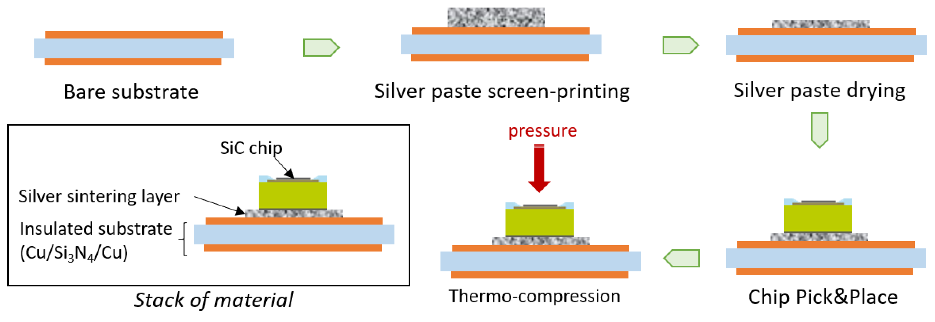
2.1. Sample Preparation and Reliability Test

The considered device under test is a molded package with silicon carbide MOSFET power devices attached on an active metal brazed (AMB) substrate by means of a sintering process shown in Figure 1. It was remarked that the molding compound injection and curing occur after sintering and it is not reported in the schematic. As depicted in this figure, paste with silver powder is screen printed on the silver plating in the front side of bare substrate. More in detail, a commercial sintering paste, made by silver powder and an organic vehicle, is used for the process. The typical dimension of silver flakes is in the order of 0.5 μm. Drying is performed to eliminate the solvent content of the paste. Then, the chip is placed by automatic equipment for pick and place on the dried silver paste. Finally, the chip is pressed by a tool applied on AlSiCu front metallization on the substrate at high temperature and for a certain time. The proposed process optimization relies on this final process step, considering three different pressure levels (p1 < p2 < p3), between 10 and 30 MPa and applied for 2 min. Temperature is fixed between 200 and 250 °C.
Porosity is a physical parameter strictly linked to the applied pressure during sintering. Porosity tends to decrease applying higher pressure [16] and impacts on the Ag sintering structural behavior in terms of elastic modulus, plasticity and ultimate tensile strength [18]. The pressure modifications affect the silver layer mechanical characteristics. Higher pressure increases the ultimate tensile strength. In contrast, the increase in sinter layer elastic modulus amplifies the thermal stress due to the coefficient of thermal expansion mismatch among chip, silver sintering joint and substrate [19]. Liquid-to-liquid thermal shock (TS) test is indeed employed to compare the reliability performances of the three different pressure values.
Such a test consists of transferring the device under test between two baths of perfluoropolyether fluid at 150 °C and −65 °C. Samples dwell three minutes at each temperature, with transfer time smaller than 10 s. The immersion in a liquid environment allows to reach a higher stress and strain rate than thermal cycles performed under air-to-air conditions. Temperature rate reached in thermal shock is comparable with the aggressive rate enhanced by application, nevertheless, such a test can represent an over-stressed condition considering that the temperature rate involves all the package and not only a limited part (i.e., the front metal e-wire source connection), such as in an application. On the other side, the thermal shock is a practical method to benchmark the performance of sintering interconnections: other methods, as the thermal cycle, are not able to stress enough of a sintering layer up to crack generation in a time-frame compatible with package development schedule.

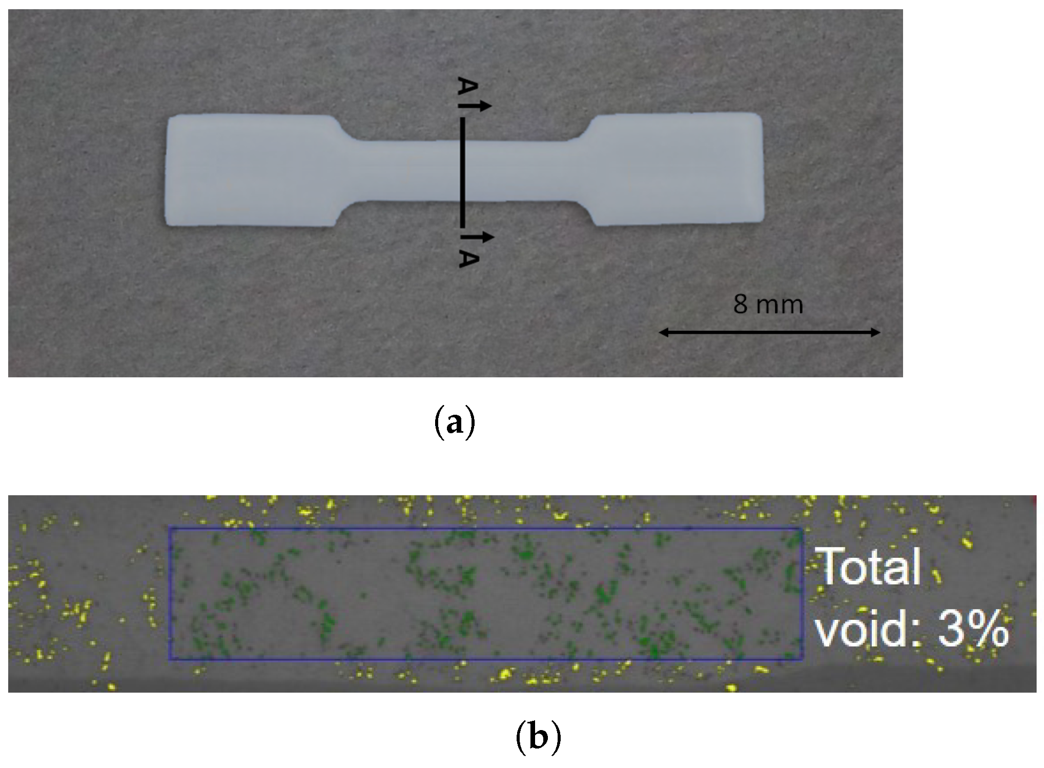
2.2. Experimental Analysis for Reliability Assessment

The porosity of a silver layer, already mentioned in Section 2.1, is measured for each analyzed sintering pressure by scanning electron microscopy (SEM) equipped with back-scattered detector. This investigation is performed on dedicated metallographic crosssections of samples without reliability stress (just after the sintering process). Microscopic pictures are processed by a dedicated software to quantify the porosity inside the sintered layer. Voids can be distinguished by silver material due to the different gray tonality: voids appear darker. SEM is also employed to detect crack occurrence in sintering joints before the reliability assessment starts and after 3000 TS for the three considered pressure parameters.
Considering that SEM is a destructive and time-consuming technique because a nonnegligible amount of time is needed for sample preparation, there is the need to search for a non-destructive and quicker methodologies. In this framework, scanning acoustic microscopy (SAM) in reflection mode is considered. In order to have accurate control over wave propagation, SAM samples are dipped in water. Due to SAM characteristics, it is possible to analyze the degradation of sintering interfaces at intermediate steps of durability stress without altering the samples.
Another methodology adopted to evaluate the degradation during reliability stress is the monitoring of a temperature-sensitive electric parameter. For MOSFET devices and fixing a sufficiently moderate current value that cannot heat the device, it has been proven that the drop voltage of body diode (VF) tends to decreases proportionally to the device temperature. Assuming to provide a given power pulse to heat the device, the difference between the VF before and after the power pulse, named ΔVF, tends to increase with higher temperature difference. This parameter is widely considered for temperature estimation of power packages and modules [20,21]. In this specific framework, ΔVF is measured 100 μs after the application of a predefined power pulse. Comparing ΔVF at the different TS aging time, it is possible to have an indication of sintering layer degradation during the reliability stress. A more delaminated layer implies the worst thermal dissipation and therefore, a higher ΔVF value directly linked with temperature swing. All the considered equipment for sintering manufacturing and reliability evaluation are resumed in Table 1.

2.3. Elastoplastic Characterization of Silver Sintering

In order to evaluate the temperature softening effect on nominally bulk sintering material, tests on dogbone samples are carried out at five different temperature: −65, 25, 100, 150 and 200 °C. The considered specimen is shown in Figure 2a. The sample width is 2 mm while the length of the narrow part is 8 mm. Sample thickness is 0.5 mm. Specimens are formed sintering silver foils applying a pressure of 20 MPa and a temperature of 250 °C for 90 s. Then, dogbone samples are cut by die pressing. Sample porosity is quantified by the software recognition method mentioned in Section 2.2. The void measurement result is reported in Figure 2b, resulting in a porosity of 3% that is reasonably close to a sample free of voids. For each thermal condition, four identical samples are tested and the average behavior is reported. Stress and strain data are obtained in displacement control, with a strain rate of 0.0015 s−1.
Loads and length are transformed in engineering and true strain/stress values by Equations (1) and (2):
ε t r u e = ln ( 1 + ε e n g )
σ t r u e = σ e n g ( 1 + ε e n g )
in which F ( t ) is the measured force by the load cell at time t, A 0 and l 0 are, respectively, the cross-section and the gauge length of the unloaded sample and l ( t ) is the gauge length. True stress and strain consider the real cross-section reduction that occurs during the tensile test, while engineering values do not consider this. Moreover, the Young modulus is measured at a different temperature using the classic method based on strain gauge [22]. For each temperature, five samples are characterized.
There is the need to implement a numerical methodology to extract silver sintering mechanical properties related to sintered layer porosity. Silver unit cells are generated by computer-aided design (CAD) software to reproduce the different arrangements of micrometric Ag-spheres according to the SEM morphological analysis depicted in Figure 3 that refers to package cross-section with a sintering layer and interface. The created silver cells with different a void fraction (8 and 20%) are reported in Figure 4.
The elastic-plastic properties are from finite element analysis (FEA) considering these cell models. The silver material is assumed to behave as the experimentally characterized elastoplastic curve, then a kind of tensile test is simulated to fix the bottom side of the cell and moving upward the top side. The elastoplastic curve is obtained, subdividing the reaction force on the fixed constraint with the imposed displacement on the cell top side.

3. Results

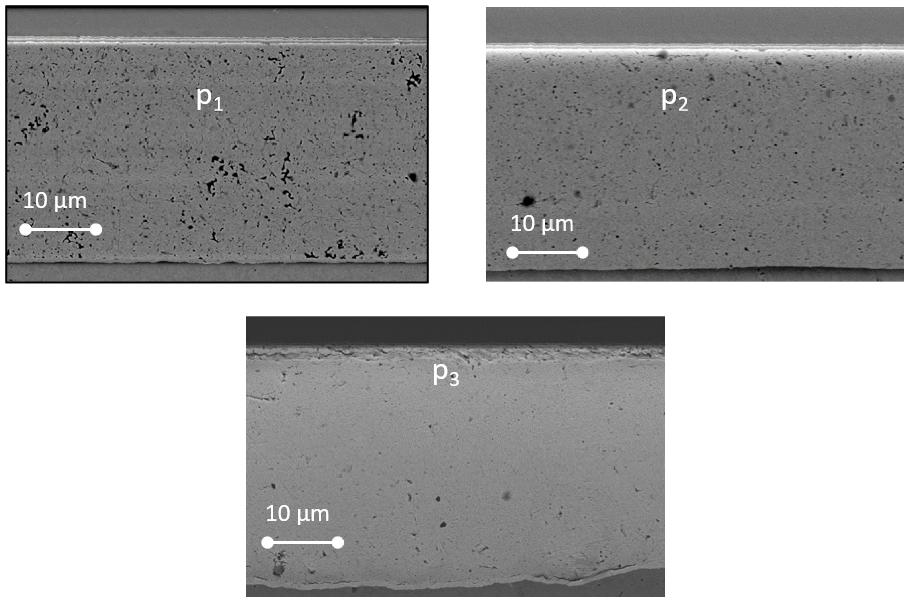
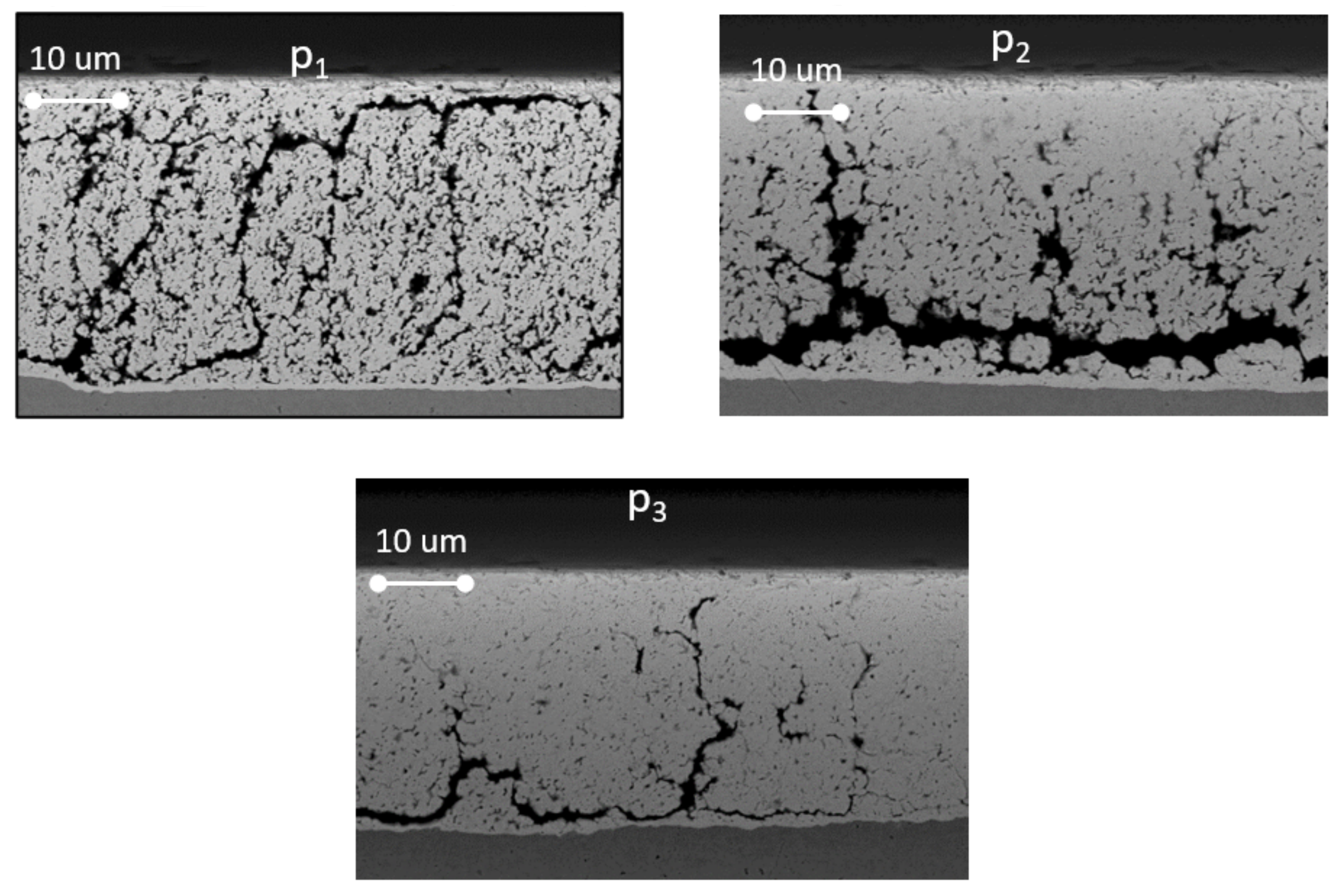
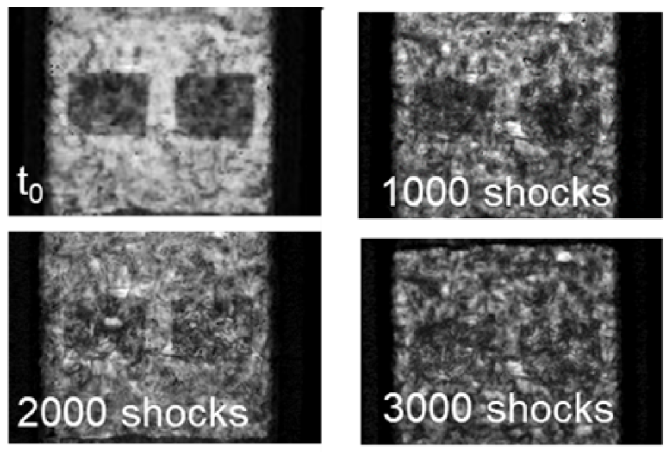
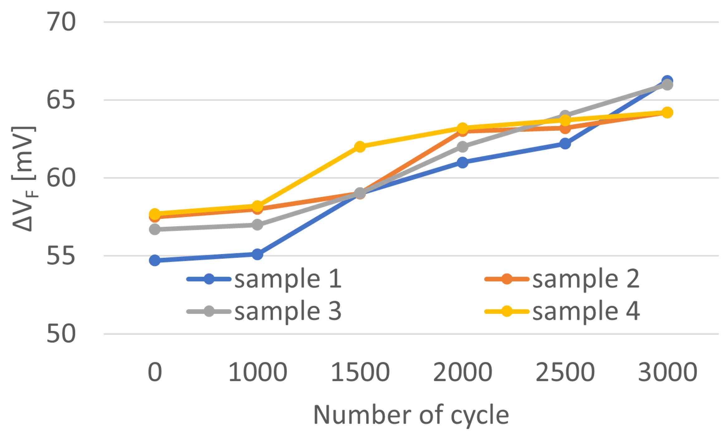
3.1. Reliability Assessment for Pressure Sintering Optimization

The porosity of the sintering layer is measured after the sintering process, as depicted in Figure 5. Voids in the sintered layer appear as black points inside the silver material. This experimental output quantifies how the porosity decreases with higher sintering pressure: for the lower sintering pressure, p1, the fraction of voids is 20%, for the intermediate value, p2, the fraction of voids is 12%, and for the maximum pressure, p3, the fraction of voids is 8%. The experimental measurement error is within the 0.5%.
SEM analyses are performed on cross-sections of virgin parts and after 3000 TS, as reported, respectively, in Figure 6 and Figure 7. The time-zero pictures show that silver sintering joints are free of crack. Such as in Figure 5, even if with less contrast due to different image acquisition setup, Figure 6 highlights that the void percentage is lower for the maximum pressure p3 according to the reduced black spots, which also, in this case, are representative of the sintering porosity. The investigation after reliability stress shows the presence of fractures in the three scenarios. From a qualitative standpoint, it is observed that the crack length is less critical considering p3. Looking to the p1 and p2 results, fractures propagate from the left to the right side while cracks are less enhanced considering the highest pressure p3. The same behavior is also observed for other sample cross-sections, which are not reported for the sake of brevity. Cross-section cracks’ length is quantified for the three scenarios. Placing equal to 1 the cracks’ length for p1, it decreases to 0.61 and 0.46 for p2 and p3, respectively. On the basis of this evidence, the sintering process has been set considering the sintering pressure p3.
For the samples assembled using the p1 value, the evolution of sintering degradation during the TS test was monitored with no destructive SAM focused on interface between AMB substrate and silver sintering. The SAM output is presented in Figure 8 at four different steps: after assembly (t0) and after 1000, 2000 and 3000 shocks. The progressive delamination is highlighted by the reduction in contrast between chips’ imprints and substrate increasing the number of cycles.
The effect of sintering degradation on thermal performance is highlighted for p1 case by the monitoring of body diode drop voltage ΔVF, as well as reported in Figure 9. In this graph, it was pointed out that ΔVF and indeed the temperature swing after power pulse application increase during liquid TS. Considering that the thermal path involves sintering layers, the degradation of thermal behavior could be explained by sintering delamination. The continuous physical monitoring of silver layer degradation represents a pillar for the development of numerical model to reproduce silver sintering aging during reliability stress.

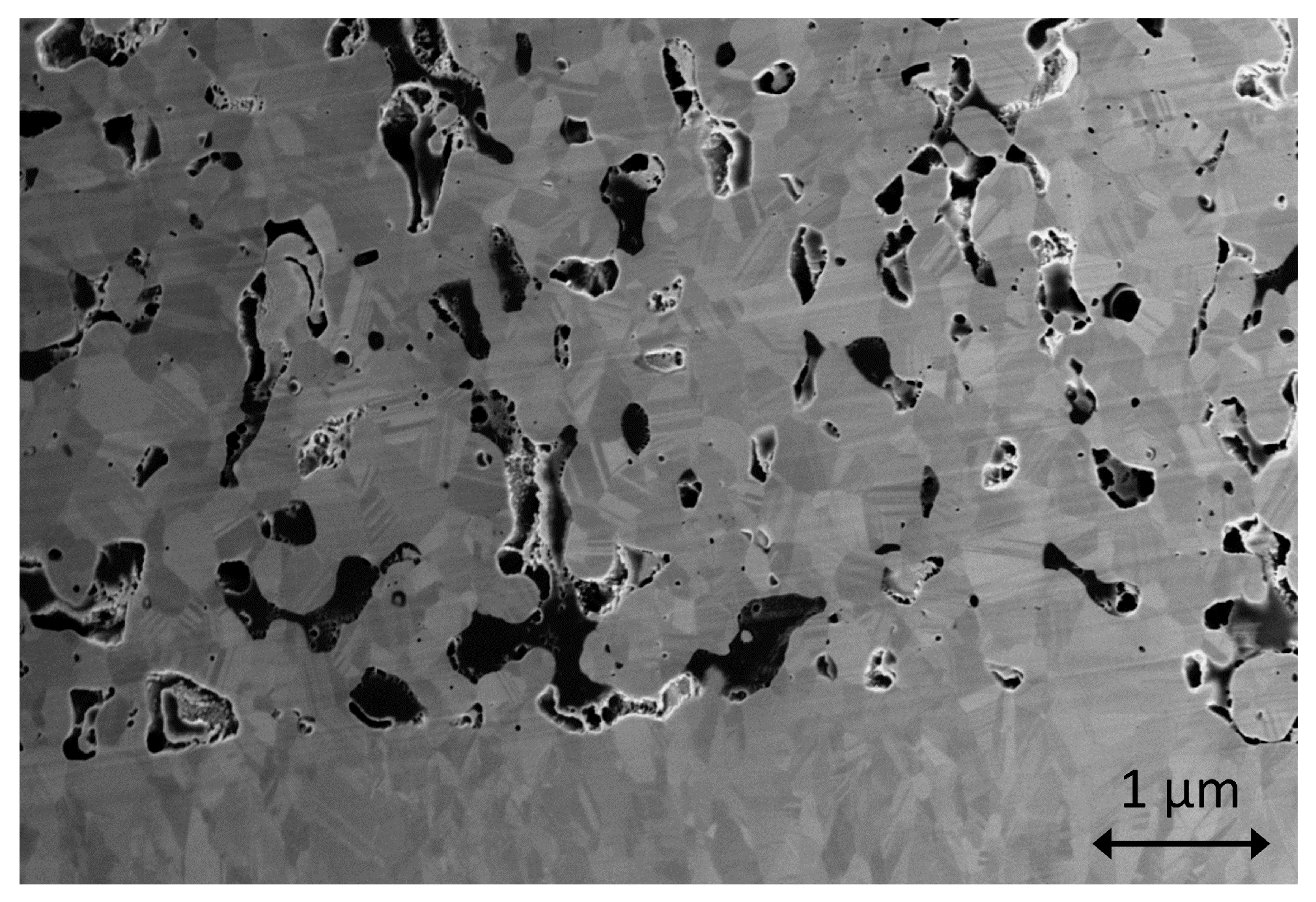
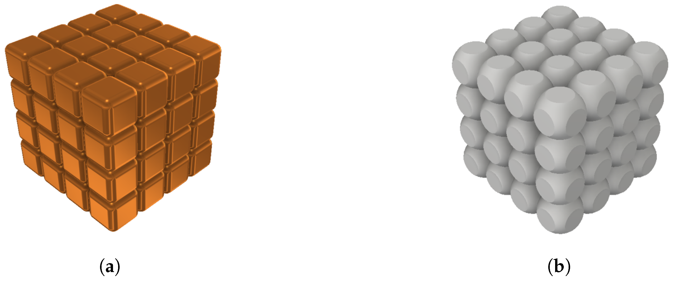
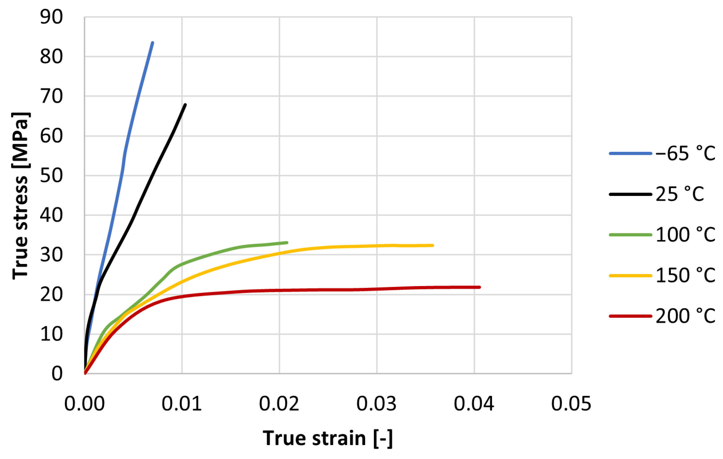
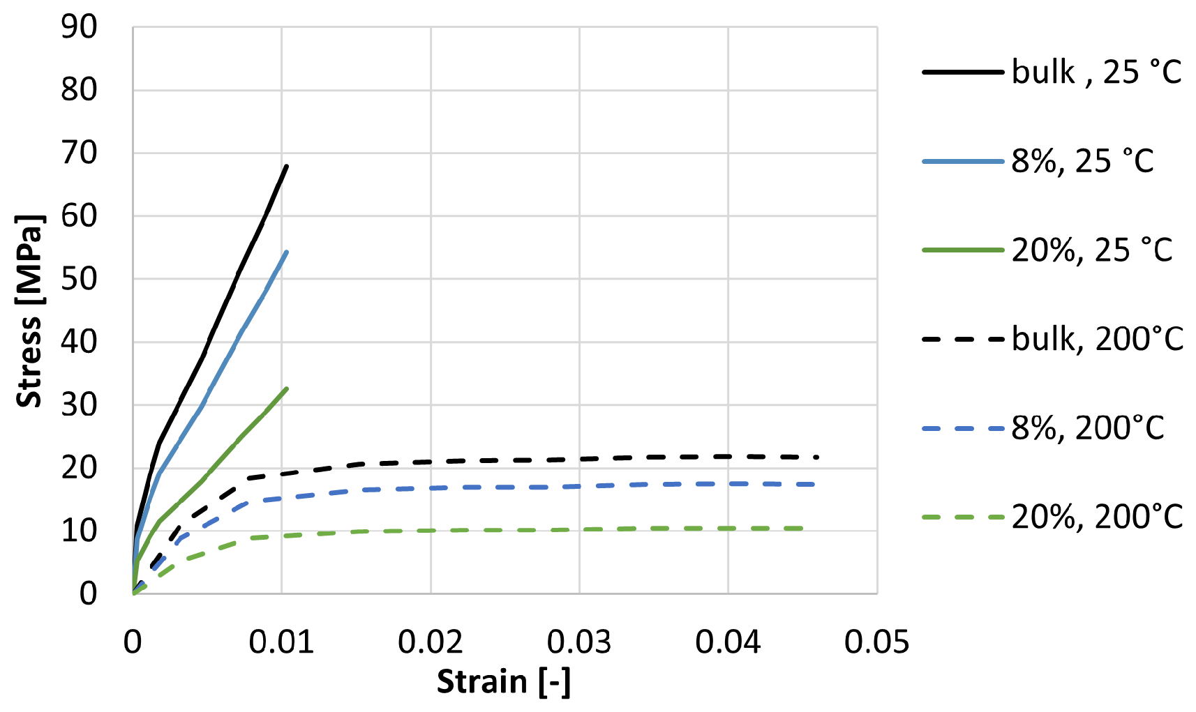
3.2. Elastoplastic Characterization Results

Elastoplastic characteristics for silver sintering are measured at different temperatures for the sample shown in Figure 2. The resulting curves are plotted in Figure 10. Material behavior becomes more brittle at low temperature, whilst it becomes more ductile and softer at high temperature, as expected by other researchers [7]. Results are reported in Table 2 showing the Young modulus decreasing at higher temperature.
As mentioned in Section 2.3, the experimental curves retrieved for the quite-bulk sample (with less than 3% of void fraction) are assumed as a starting point for the finite element simulation of mechanical response of sintering layer with a certain porosity percentage. Numerical outcomes are plotted in Figure 11. Coherently with assumptions, it is possible to observe that the “bulk” curves of Figure 11 are the same that “ 25 °C ” and “ 200 °C ” of Figure 10. FEA simulations highlight and quantify how the porosity inside the sintering material reduce the layer stiffness resulting in lower elastic modulus and yield values. This finding is aligned with a literature experimental characterization [18] of a silver sintering layer as function of material density. The proposed model does not calculate the ultimate tensile strength which is expected to decrease with higher void fraction [18]. This fact is not a limitation considering that presented simulation curves are applied for reliability simulations in which strain and stress are much lower than ultimate values. In fact, the performed experimental-numerical characterization would serve to define the input in terms of silver sintering material properties for modeling activities aiming to perform a reliability forecast.

4. Conclusions

The presented activity has proposed an experimental methodology for the optimization of the pressure of the silver sintering die attach process. The assessment was based on a liquid-to-liquid thermal shock (TS) test and on dedicated physical analyses (SEM, SAM and electric measurements) aiming to check and monitor sintering layer degradation during the reliability stress. Considering that the effect of three different pressure values has been analyzed, the porosity fraction has been identified as the main representative physical parameter. The employed investigation has highlighted that the maximum pressure value p3 leads to the best reliability performances. In the framework of process characterization, two non-destructive techniques (SAM and electric measurements) were proposed that can analyze how delamination evolves with TS. Moreover, a dedicated uniaxial tensile test was employed to characterize the stress–strain behavior of almost-bulk (free of voids) silver sintering samples at different temperatures ranging from −65 to 200 °C. This experimental characterization acted as a starting point to simulate the mechanical behavior of a silver sintering joint—with a defined percentage of void and without the need of dedicated uniaxial tests for a specific void ratio—via finite element analysis (FEA).
The mentioned capability to simulate the elasto-plastic behavior as a function of void percentage in sintering layer is needed to perform the FEA simulation of material degradation due to a reliability stress such as TS. Porosity is a parameter that can be quantified; therefore. the proposed simulation method allows to account for the real silver sintering properties. It is of paramount interest that the virtual characterization of sintering material considers the same average of a void fraction but a different or irregular silver pattern. Since it is expected that elastic properties mainly depend on porosity average, this investigation may highlight different plastic behaviors. A further development of the presented activity will be the virtual simulation of the degradation during thermal shock. The implementation of a multiscale modeling approach, such as the “global–local” model, can support this specific purpose. Such a technique allows the calculation of deformation by a “global” model that represents the entire package, meanwhile, stress on the sintering layer is computed by a “local” model that takes “global” deformation as input.Once the model is calibrated step by step with physical evidence such as the presented SAM and electric measurements, the creation of a finite element model permits to reduce the time needed for future assessment and to make very accurate analyses in terms of geometry and time resolution. Moreover, interface analysis can be enriched by the characterization of sintering adhesion properties and relevant fracture mode-mixity, which can be achieved by performing a set of experiments on dedicated specimens and applying an advanced theoretical model such as the cohesive zone model (CZM) [23].

Author Contributions

Conceptualization, G.S.; data curation, M.C.; investigation, A.S.; methodology, M.C.; supervision, S.M.O. and G.S.; validation, M.C.; writing—original draft, A.S. All authors have read and agreed to the published version of the manuscript.

Funding

This paper belongs to a research path funded by Regione Sicilia (Azione 1.2.1_ 03 del PO FESR SICILIA 2014-2020 – Progetto PON03PE_00206_1 AMELIE “Advanced framework for Manufacturing Engineering and product Lifecycle Enhancement.” CUP G76I20000060007).

Institutional Review Board Statement

Not applicable.

Informed Consent Statement

Not applicable.

Conflicts of Interest

The authors declare no conflict of interest.

Abbreviations

The following abbreviations are used in this manuscript:
AMBActive Metal Brazed
CADComputer Aided Design
CZMCohesive Zone Model
FEAFinite Element Analysis
SAMScanning Acoustic Microscopy
SEMScanning Electron Microscopy
TSThermal Shock

References

  1. Luo, H.; Iannuzzo, F.; Blaabjerg, F.; Li, W.; He, X. Separation test method for investigation of current density effects on bond wires of SiC power MOSFET modules. In Proceedings of the IECON 2017—43rd Annual Conference of the IEEE Industrial Electronics Society, Beijing, China, 29 October–1 November 2017; pp. 1525–1530. [Google Scholar] [CrossRef]
  2. ECPE Guideline AQG 324—Qualification of Power Modules for Use in Power Electronics Converter Units in Motor Vehicles; Standard; ECPE European Center for Power Electronics: Nuremberg, Germany, 2021.
  3. Klaka, S.; Sittig, R. Reduction of thermomechanical stress by applying a low temperature joining technique. In Proceedings of the 6th International Symposium on Power Semiconductor Devices and Ics, Davos, Switzerland, 31 May–2 June 1994; pp. 259–264. [Google Scholar] [CrossRef]
  4. Göbl, C.; Faltenbacher, J. Low temperature sinter technology die attachment for power electronic applications. In Proceedings of the 2010 6th International Conference on Integrated Power Electronics Systems, Niagara Falls, ON, Canada, 11–13 October 2010; pp. 1–5. [Google Scholar]
  5. Schmitt, W.; Chew, L.M. Silver sinter paste for SiC bonding with improved mechanical properties. In Proceedings of the 2017 IEEE 67th Electronic Components and Technology Conference (ECTC), Orlando, FL, USA, 30 May–2 June 2017; pp. 1560–1565. [Google Scholar]
  6. Weber, C.; Walter, H.; Dijk, M.V.; Hutter, M.; Wittler, O.; Lang, K.D. Combination of Experimental and Simulation Methods for Analysis of Sintered Ag Joints for High Temperature Applications. In Proceedings of the 2016 IEEE 66th Electronic Components and Technology Conference (ECTC), Las Vegas, NV, USA, 31 May–3 June 2016; pp. 1335–1341. [Google Scholar] [CrossRef]
  7. Schaal, M.; Klingler, M.; Wunderle, B. Silver Sintering in Power Electronics: The State of the Art in Material Characterization and Reliability Testing. In Proceedings of the 2018 7th Electronic System-Integration Technology Conference (ESTC), Dresden, Germany, 18–21 September 2018; pp. 1–18. [Google Scholar]
  8. Knoerr, M.; Kraft, S.; Schletz, A. Reliability assessment of sintered nano-silver die attachment for power semiconductors. In Proceedings of the 2010 12th Electronics Packaging Technology Conference, Singapore, 8–10 December 2010; pp. 56–61. [Google Scholar] [CrossRef]
  9. Calabretta, M.; Sitta, A.; Oliveri, S.M.; Sequenzia, G. Design and process optimization of a sintered joint for power electronics automotive applications. In Proceedings of the International Conference on Design, Simulation, Manufacturing: The Innovation Exchange, Modena, Italy, 9–10 September 2019; Springer: New York, NY, USA, 2019; pp. 470–480. [Google Scholar]
  10. Knoerr, M.; Schletz, A. Power semiconductor joining through sintering of silver nanoparticles: Evaluation of influence of parameters time, temperature and pressure on density, strength and reliability. In Proceedings of the 2010 6th International Conference on Integrated Power Electronics Systems, Nuremberg, Germany, 16–18 March 2010; pp. 1–6. [Google Scholar]
  11. Dudek, R.; Döring, R.; Sommer, P.; Seiler, B.; Kreyssig, K.; Walter, H.; Becker, M.; Günther, M. Combined Experimental- and FE-Studies on Sinter-Ag Behaviour and Effects on IGBT-Module Reliability. In Proceedings of the 2014 15th International Conference on Thermal, Mechanical and Mulit-Physics Simulation and Experiments in Microelectronics and Microsystems (EuroSimE), Ghent, Belgium, 7–9 April 2014; pp. 1–9. [Google Scholar]
  12. Ying, L.C.; Fei, C.C. Temperature cycling and thermal shock correlation in DPAK & DSO packages. In Proceedings of the 2012 10th IEEE International Conference on Semiconductor Electronics (ICSE), Kuala Lumpur, Malaysia, 19–21 September 2012; pp. 458–461. [Google Scholar] [CrossRef]
  13. Liu, C.; Brem, F.; Riedel, G.; Eichelberger, E.; Hofmann, N. The influence of thermal cycling methods on the interconnection reliability evaluation within IGBT modules. In Proceedings of the 2012 4th Electronic System-Integration Technology Conference, Amsterda, The Netherlands, 17–20 September 2012; pp. 1–5. [Google Scholar] [CrossRef]
  14. Huang, Y.; Luo, Y.; Xiao, F.; Liu, B. Failure Mechanism of Die-Attach Solder Joints in IGBT Modules under Pulse High-Current Power Cycling. IEEE J. Emerg. Sel. Top. Power Electron. 2019, 7, 99–107. [Google Scholar] [CrossRef]
  15. Herboth, T.; Früh, C.; Günther, M.; Wilde, J. Assessment of thermo-mechanical stresses in low temperature joining technology. In Proceedings of the 2012 13th International Thermal, Mechanical and Multi-Physics Simulation and Experiments in Microelectronics and Microsystems, Cascais, Portugal, 16–18 April 2012; pp. 1–7. [Google Scholar]
  16. Herboth, T.; Guenther, M.; Fix, A.; Wilde, J. Failure mechanisms of sintered silver interconnections for power electronic applications. In Proceedings of the 2013 IEEE 63rd Electronic Components and Technology Conference, Las Vegas, NV, USA, 28–31 May 2013; pp. 1621–1627. [Google Scholar]
  17. Calabretta, M.; Renna, M.; Vinciguerra, V.; Messina, A.A. Power packages interconnections for high reliability automotive applications. In Proceedings of the ESSDERC 2019—49th European Solid-State Device Research Conference (ESSDERC), Cracow, Poland, 23–26 September 2019; pp. 35–39. [Google Scholar] [CrossRef]
  18. Caccuri, V.; Milhet, X.; Gadaud, P.; Bertheau, D.; Gerland, M. Mechanical Properties of Sintered Ag as a New Material for Die Bonding: Influence of the Density. J. Electron. Mater. 2014, 43, 4510–4514. [Google Scholar] [CrossRef]
  19. Herold, C.; Sun, J.; Seidel, P.; Tinschert, L.; Lutz, J. Power cycling methods for SiC MOSFETs. In Proceedings of the 2017 29th International Symposium on Power Semiconductor Devices and IC’s (ISPSD), Sapporo, Japan, 28 May–1 June 2017; pp. 367–370. [Google Scholar]
  20. Lutz, J.; Franke, J. Reliability and reliability investigation of wide-bandgap power devices. Microelectron. Reliab. 2018, 88, 550–556. [Google Scholar] [CrossRef]
  21. Funaki, T.; Fukunaga, S. Difficulties in characterizing transient thermal resistance of SiC MOSFETs. In Proceedings of the 2016 22nd International Workshop on Thermal Investigations of ICs and Systems (THERMINIC), Budapest, Hungary, 21–23 September 2016; pp. 141–146. [Google Scholar] [CrossRef]
  22. A Review of Contacting Strain Measurement Techniques for Composites Laminate Testing. Available online: https://www.instron.com/-/media/literature-library/whitepapers/2014/07/contacting-strain-measurements-techniques.pdf (accessed on 21 July 2021).
  23. Krieger, W.E.; Raghavan, S.; Sitaraman, S.K. Experiments for Obtaining Cohesive-Zone Parameters for Copper-Mold Compound Interfacial Delamination. IEEE Trans. Components Packag. Manuf. Technol. 2016, 6, 1389–1398. [Google Scholar] [CrossRef]
Figure 1. Schematic of the process flow for silver sintering process and the stack of the material at the end of sintering process.
Applsci 11 07012 g001
Figure 2. Utilized sample for the tensile test: (a) and void measurement in section A–A (b).
Applsci 11 07012 g002
Figure 3. SEM picture of an FIB cut showing the morphological details of the sintering layer’s microstructural texture.
Applsci 11 07012 g003
Figure 4. Cell models of sintering grain reproducing the micro-mechanical structure for two porosity values: 8% (a) and 20% (b).
Applsci 11 07012 g004
Figure 5. Quantification of porosity fraction by SEM for the three sintering pressures.
Applsci 11 07012 g005
Figure 6. SEM analysis on sample cross-sections after the sintering process for the three considered sintering pressures.
Applsci 11 07012 g006
Figure 7. SEM analysis on sample cross-sections after 3000 TS for the three considered sintering pressures.
Applsci 11 07012 g007
Figure 8. SAM analysis of the interface between silver sintering and the AMB substrate at different steps of TS stress (time zero t0, after 1000, 2000 and 3000 shocks). The contrast modifications between chips’ imprints (in black) and substrate (white) indicate interface delamination.
Applsci 11 07012 g008
Figure 9. ΔVF drift during thermal shocks, for four samples assembled with sintering pressure equal to p1 and at a different number of thermal shocks (0, 1000, 1500, 2000, 2500 and 3000).
Applsci 11 07012 g009
Figure 10. Stress–strain characteristic at different temperature.
Applsci 11 07012 g010
Figure 11. Simulated stress–strain curves at 25 (continuous lines) and 200 °C (dashed lines) for silver bulk and for two different Ag sintering layer porosity (8 and 20%).
Applsci 11 07012 g011
Table 1. Considered equipment for experiments.
TaskEquipmentSupplier
SinteringSinterstar InnovateBoschmann
F-XL
SAMEcho LSSonix
SEMNeon 40Zeiss
Electric measurement4324-KTTesec
Table 2. Experimental average ± standard deviation of the Young modulus at different temperature. Five samples are considered for each temperature level.
Temperature (°C)Young Modulus (GPa)
−65186 ± 6
2560 ± 4
10032 ± 3
15021 ± 3
20011 ± 2
Publisher’s Note: MDPI stays neutral with regard to jurisdictional claims in published maps and institutional affiliations.

