
Warpage Behavior on Silicon Semiconductor Device: The Impact of Thick Copper Metallization


Abstract
1. Introduction
2. Sample and Test Description
3. Warpage Measurements and Physical Analysis
3.1. Method Description for Warpage Measurements
3.2. Results
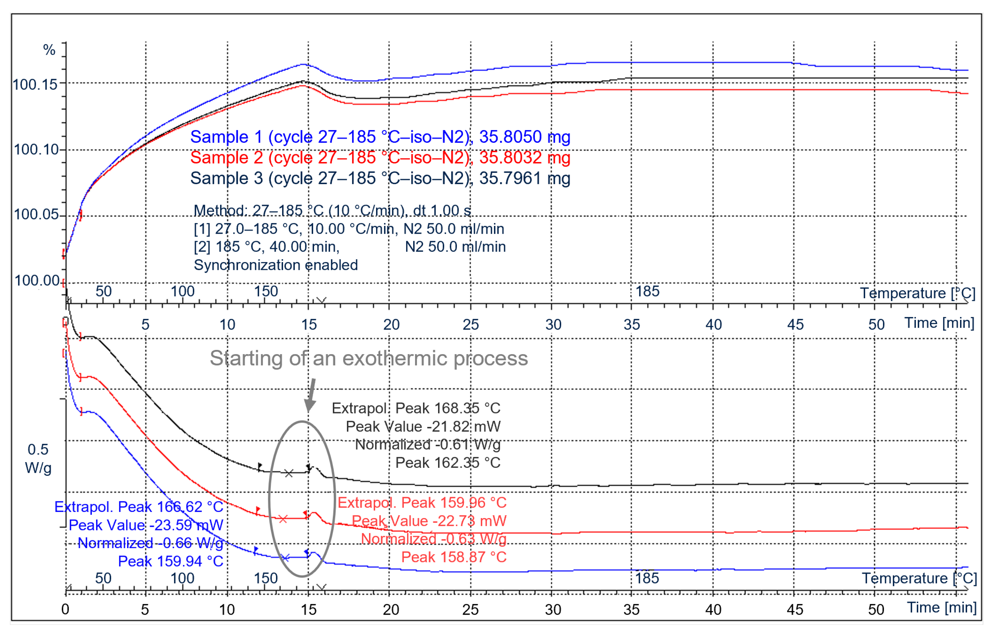
3.3. Physical Analysis
4. Model for Warpage Calculation
4.1. Literature Analytical Approaches
4.2. Finite Element Model for Warpage Calculation
5. Conclusions
Author Contributions
Funding
Institutional Review Board Statement
Informed Consent Statement
Data Availability Statement
Conflicts of Interest
References
- Nelhiebel, M.; Illing, R.; Detzel, T.; Wöhlert, S.; Auer, B.; Lanzerstorfer, S.; Rogalli, M.; Robl, W.; Decker, S.; Fugger, J.; et al. Effective and reliable heat management for power devices exposed to cyclic short overload pulses. Microelectron. Reliab. 2013, 53, 1745–1749. [Google Scholar] [CrossRef]
- Huang, R.; Robl, W.; Dehm, G.; Ceric, H.; Detzel, T. Disparate tendency of stress evolution of thin and thick electroplated Cu films at room temperature. In Proceedings of the 2010 17th IEEE International Symposium on the Physical and Failure Analysis of Integrated Circuits, Singapore, 5–9 July 2010; pp. 1–6. [Google Scholar] [CrossRef]
- Du, S.; Li, Y. Effect of Annealing on Microstructure and Mechanical Properties of Magnetron Sputtered Cu Thin Films. Adv. Mater. Sci. Eng. 2015, 2015, 1–8. [Google Scholar] [CrossRef]
- Calabretta, M.; Sitta, A.; Oliveri, S.M.; Sequenzia, G. An experimental-numeric approach to manufacture semiconductor wafer using thick copper front metallization. Int. J. Interact. Des. Manuf. IJIDeM 2020. [Google Scholar] [CrossRef]
- Wang, F.; Zhao, Z.; Nie, N.; Wang, F.; Zhu, W. Dynamic through-silicon-via filling process using copper electrochemical deposition at different current densities. Sci. Rep. 2017, 7, 46639. [Google Scholar] [CrossRef] [PubMed]
- Kauffman, J.; Gilbert, J.; Paterson, E. Multi-Physics Modeling of Electrochemical Deposition. Fluids 2020, 5, 240. [Google Scholar] [CrossRef]
- Chen, J.; Degryse, D.; Ratchev, P.; Wolf, I.D. Mechanical issues of Cu-to-Cu wire bonding. IEEE Trans. Compon. Packag. Technol. 2004, 27, 539–545. [Google Scholar] [CrossRef]
- Jeon, J.; Na, S.; Jeon, S.; Mo, M.; Kang, D.; Lim, K.; Kim, J. High reliability challenges with Cu wire bonding for automotive devices in the AEC-Q006. In Proceedings of the 2017 IEEE 67th Electronic Components and Technology Conference (ECTC), Orlando, FL, USA, 30 May–2 June 2017; pp. 1968–1973. [Google Scholar] [CrossRef]
- Chauhan, P.S.; Choubey, A.; Zhong, Z.; Pecht, M.G. (Eds.) Copper wire bonding. In Copper Wire Bonding; Springer: New York, NY, USA, 2014; pp. 1–9. [Google Scholar] [CrossRef]
- Bai, X.; Chang, B.; Du, D. Influences of material and structural factors on the stress conditions in Cu/low-k chips during Cu wire bonding. In Proceedings of the 2014 15th International Conference on Electronic Packaging Technology, Chengdu, China, 12–15 August 2014; pp. 441–446. [Google Scholar] [CrossRef]
- Auersperg, J.; Breuer, D.; Machani, K.V.; Rzepka, S.; Michel, B. FEA study of damage and cracking risks in BEoL structures under copper wirebonding impact. In Proceedings of the 2015 16th International Conference on Thermal, Mechanical and Multi-Physics Simulation and Experiments in Microelectronics and Microsystems, Budapest, Hungary, 19–22 April 2015; pp. 1–5. [Google Scholar] [CrossRef]
- Calabretta, M.; Guarnera, D.; Sitta, A.; Renna, M.; Sciuto, A.; D’Arrigo, G.; Oliveri, S.M.; Sequenzia, G. Mechanical characterization and modeling of different pad structures. In Proceedings of the 2020 21st International Conference on Thermal, Mechanical and Multi-Physics Simulation and Experiments in Microelectronics and Microsystems (EuroSimE), Cracow, Poland, 5–8 July 2020; pp. 1–5. [Google Scholar] [CrossRef]
- Cheng, G.; Xu, G.; Gai, W.; Luo, L. Influence of observed anelasticity of Cu on the wafer warpage evolution during thermal processes. In Proceedings of the 2018 19th International Conference on Electronic Packaging Technology (ICEPT), Shanghai, China, 8–11 August 2018; pp. 1119–1122. [Google Scholar] [CrossRef]
- Durand, C.; Klingler, M.; Coutellier, D.; Naceur, H. Power Cycling Reliability of Power Module: A Survey. IEEE Trans. Device Mater. Reliab. 2016, 16, 80–97. [Google Scholar] [CrossRef]
- Russo, S.; Bazzano, G.; Cavallaro, D.; Sitta, A.; Calabretta, M. Thermal analysis approach for predicting power device lifetime. IEEE Trans. Device Mater. Reliab. 2019, 19, 159–163. [Google Scholar] [CrossRef]
- Sitta, A.; Russo, S.; Bazzano, G.; Cavallaro, D.; Greco, G.; Calabretta, M. Numerical approach to predict power device reliability. In Proceedings of the 2018 13th International Conference on Design & Technology of Integrated Systems in Nanoscale Era (DTIS), Taormina, Italy, 9–12 April 2018; pp. 1–5. [Google Scholar] [CrossRef]
- Bayerer, R.; Herrmann, T.; Licht, T.; Lutz, J.; Feller, M. Model for Power Cycling lifetime of IGBT Modules—Various factors influencing lifetime. In Proceedings of the 5th International Conference on Integrated Power Electronics Systems, Nuremberg, Germany, 11–13 March 2008; pp. 1–6. [Google Scholar]
- Ciappa, M. Selected failure mechanisms of modern power modules. Microelectron. Reliab. 2002, 42, 653–667. [Google Scholar] [CrossRef]
- Calabretta, M.; Sitta, A.; Oliveri, S.M.; Sequenzia, G. Power Semiconductor Devices and Packages: Solder Mechanical Characterization and Lifetime Prediction. IEEE Access 2021, 9, 22859–22867. [Google Scholar] [CrossRef]
- Castoldi, L.; Morin, S.; Visalli, G.; Fukada, T.; Ouaknine, M.; Roh, E.; Yoo, W. Annealing characteristics of copper films for power device applications. In Thin Film Materials, Processes, and Reliability: Plasma Processing for the 100 Nm Node and Copper Interconnects with Low-k Inter-Level Dielectric Films: Proceedings of the International Symposium; The Electrochemical Society: Pennington, NJ, USA, 2003; Volume 2003, p. 330. [Google Scholar]
- Timoshenko, S. Analysis of bi-metal thermostats. Josa 1925, 11, 233–255. [Google Scholar] [CrossRef]
- Stoney, G.G. The tension of metallic films deposited by electrolysis. Proc. R. Soc. Lond. Ser. A Contain. Pap. Math. Phys. Character 1909, 82, 172–175. [Google Scholar] [CrossRef]
- Weidmann, D.; Dubois, G.; Hertl, M.; Chauffleur, X. Determination of strength of interface in packages based on an approach using coupling of experimental and modeling results. In Proceedings of the 2011 12th International Conference on Thermal, Mechanical & Multi-Physics Simulation and Experiments in Microelectronics and Microsystems, Linz, Austria, 18–20 April 2011; pp. 1–6. [Google Scholar] [CrossRef]
- Degrieck, J.; Van Paepegem, W.; Boone, P. Application of digital phase-shift shadow moiré to micro deformation measurements of curved surfaces. Opt. Lasers Eng. 2001, 36, 29–40. [Google Scholar] [CrossRef]
- Mancaleoni, A.; Sitta, A.; Colombo, A.; Villa, R.; Mirone, G.; Renna, M.; Calabretta, M. Copper wire bonding process characterization and simulation. In Proceedings of the CIPS 2020 11th International Conference on Integrated Power Electronics Systems, Berlin, Germany, 24–26 March 2020; pp. 1–4. [Google Scholar]
- Chaudhari, P. Grain growth and stress relief in thin films. J. Vac. Sci. Technol. 1972, 9, 520–522. [Google Scholar] [CrossRef]
- Ostrowicki, G.T.; Gurrum, S.P.; Nangia, A. Correlated model for wafer warpage prediction of arbitrarily patterned films. In Proceedings of the 2018 IEEE 68th Electronic Components and Technology Conference (ECTC), San Diego, CA, USA, 29 May–1 June 2018; pp. 2116–2120. [Google Scholar] [CrossRef]
- Bigl, S.; Wurster, S.; Cordill, M.; Kiener, D. Substrate-Influenced Thermo-Mechanical Fatigue of Copper Metallizations: Limits of Stoney’s Equation. Materials 2017, 10, 1287. [Google Scholar] [CrossRef] [PubMed]
- Vasudevan, M.; Johnson, W. Thermal Bending of a Tri-Metal Strip. Aeronaut. J. 1961, 65, 507–509. [Google Scholar] [CrossRef]
- Vasudevan, M.; Johnson, W. On multi-metal thermostats. Appl. Sci. Res. Sect. B 1961, 9, 420–430. [Google Scholar] [CrossRef]
- Sitta, A.; Renna, M.; Messina, A.A.; Mirone, G.; D’Arrigo, G.; Calabretta, M. Power module ceramic substrates: Mechanical characterization and modeling. In Proceedings of the 2020 21st International Conference on Thermal, Mechanical and Multi-Physics Simulation and Experiments in Microelectronics and Microsystems (EuroSimE), Cracow, Poland, 5–8 July 2020; pp. 1–5. [Google Scholar] [CrossRef]


| Material | Young’s Modulus GPa | CTE ppm/K | Poisson Ratio |
|---|---|---|---|
| Silicon | 120 | 2.5 | 0.28 |
| Copper | 77.5 | 16.4 | 0.364 |
| Method | Experimental | FEM | Timoshenko | Stoney |
|---|---|---|---|---|
| Warpage [m/C] | 0.700 | 0.660 | 0.605 | 0.632 |
| Stress [MPa/C] | n.a. | 1.683 | 1.003 | 1.075 |
Publisher’s Note: MDPI stays neutral with regard to jurisdictional claims in published maps and institutional affiliations. |
© 2021 by the authors. Licensee MDPI, Basel, Switzerland. This article is an open access article distributed under the terms and conditions of the Creative Commons Attribution (CC BY) license (https://creativecommons.org/licenses/by/4.0/).
Share and Cite
Calabretta, M.; Sitta, A.; Oliveri, S.M.; Sequenzia, G. Warpage Behavior on Silicon Semiconductor Device: The Impact of Thick Copper Metallization. Appl. Sci. 2021, 11, 5140. https://doi.org/10.3390/app11115140
Calabretta M, Sitta A, Oliveri SM, Sequenzia G. Warpage Behavior on Silicon Semiconductor Device: The Impact of Thick Copper Metallization. Applied Sciences. 2021; 11(11):5140. https://doi.org/10.3390/app11115140
Chicago/Turabian StyleCalabretta, Michele, Alessandro Sitta, Salvatore Massimo Oliveri, and Gaetano Sequenzia. 2021. "Warpage Behavior on Silicon Semiconductor Device: The Impact of Thick Copper Metallization" Applied Sciences 11, no. 11: 5140. https://doi.org/10.3390/app11115140
APA StyleCalabretta, M., Sitta, A., Oliveri, S. M., & Sequenzia, G. (2021). Warpage Behavior on Silicon Semiconductor Device: The Impact of Thick Copper Metallization. Applied Sciences, 11(11), 5140. https://doi.org/10.3390/app11115140