Abstract
Hardware-in-the-loop (HIL) simulations of power converters must achieve a truthful representation in real time with simulation steps on the order of microseconds or tens of nanoseconds. The numerical solution for the differential equations that model the state of the converter can be calculated using the fourth-order Runge–Kutta method, which is notably more accurate than Euler methods. However, when the mathematical error due to the solver is drastically reduced, other sources of error arise. In the case of converters that use deadtimes to control the switches, such as any power converter including half-bridge modules, the inductor current reaching zero during deadtimes generates a model error large enough to offset the advantages of the Runge–Kutta method. A specific model is needed for such events. In this paper, an approximation is proposed, where the time step is divided into two semi-steps. This serves to recover the accuracy of the calculations at the expense of needing a division operation. A fixed-point implementation in VHDL is proposed, reusing a block along several calculation cycles to compute the needed parameters for the Runge–Kutta method. The implementation in a low-cost field-programmable gate arrays (FPGA) (Xilinx Artix-7) achieves an integration time of s. The calculation errors are six orders of magnitude smaller for both capacitor voltage and inductor current for the worst case, the one where the current reaches zero during the deadtimes in 78% of the simulated cycles. The accuracy achieved with the proposed fixed point implementation is very close to that of 64-bit floating point and can operate in real time with a resolution of s. Therefore, the results show that this approach is suitable for modeling converters based on half-bridge modules by using FPGAs. This solution is intended for easy integration into any HIL system, including commercial HIL systems, showing that its application even with relatively high integration steps (s) surpasses the results of techniques with even faster integration steps that do not take these events into account.
1. Introduction
HIL (hardware-in-the-loop) techniques are being increasingly used for testing and simulation of complex systems, such as power electronics [1,2,3,4] and mechanical elements [5,6,7,8]. These techniques consist in replacing an element of the real system with a model. For instance, in [4], a photovoltaic panel with a DC–DC boost converter is modeled. The HIL model usually operates in real time and provides feedback to the rest of the system as close as possible to that of the real element, including extreme cases. This serves to identify malfunctions or bugs in the controller without causing accidents, including bodily harm or damage to equipment. A typical use in power electronic converters is testing a real implementation of the controller with a simulated plant. In case the controller puts the plant in a forbidden or dangerous state, there are no catastrophic results for the test. As an example, ref. [9] models a three-phase converter for electric vehicles along with its controller.
Although first HIL systems were implemented by using computers [10], reaching simulation steps of tens of microseconds, most of the current HIL systems use field-programmable gate arrays (FPGAs) [11,12,13], including commercial systems such as Opal-RT, dSPACE, and Typhoon HIL, among others. In the literature, it is also common to find FPGA-based HIL systems based on platforms that were not designed explicitly for HIL purposes, such s NI LabView, but reached good results [4,14]. The main advantage of FPGAs is that they have a parallel architecture, where many complex operations can be performed simultaneously. Consequently, FPGA-based systems can reach simulation steps around hundreds of ns. For instance, HIL602 system by Typhoon HIL reaches 500 ns, and even the simple model like a boost converter using a basic ODE (Ordinary Differential Equation) solver reached a simulation step of 14 ns in [15].
The HIL model usually must operate in real time and must provide acceptable accuracy. The former implies that calculation of the state variables is performed with integration times between a few microseconds and tens of nanoseconds, in order to provide a very small calculation delay and be able to emulate medium- to high-frequency converters. The latter means that the algorithms must describe with high detail the behavior of the replaced system, and the state variables must be able to encode with high accuracy the values of the physical magnitudes they represent. These are two conflicting conditions (high-speed calculation versus accurate algorithms and solvers) that lead to trade-offs in the design.
Most real-time HIL systems use linear numerical methods, such as first-order forward Euler, because of their simplicity [15,16]. However, some proposals introduce higher-order methods such as the second-order Adams–Bashforth [17,18,19] or Runge–Kutta methods [20,21]. If a model is to be integrated into a commercial system with a simulation step of around s, the Euler method could be impractical for some applications, so more accurate methods are usually utilized. High-order methods improve drastically the accuracy with the drawback of increasing the complexity and the simulation step.
As the accuracy of the simulation is improved by reducing the simulation step or using an accurate method, other sources of error become visible and limit the accuracy of the system. Some examples of these sources are small electrical losses [22] and resolution issues in the calculation of variables [23]. Another issue is found in [24], where a synchronous buck converter model does not benefit from 4th-order methods when the current reaches zero during the switching deadtime. This problem arises for any power converter using half-bridge modules, not only synchronous buck converters, because the problem comes from the fact that deadtimes are included. This paper proposes a method to solve this issue, reaching high accuracy even in those situations. The proposed method can be applied not only to synchronous buck converters but also to any converters using half-bridge modules, such as half or full-bridges, including three-phase versions.
The rest of the paper is organized as follows: Section 2 presents the modeling of the buck converter and the numerical method for solving the state equations. Section 3 discusses the sources of errors in the modeling of the circuit. Section 4 proposes an approximation to solve the errors caused by incorrect modeling of the inductor current in specific situations. Section 5 describes the simulation results obtained with the different algorithms proposed. It also describes a pipelined implementation of the numerical method and shows the time and occupation results in the proposed FPGA device. Finally, Section 6 shows the conclusions.
2. Buck Converter Modeling
The power converter used as example application is a synchronous buck converter with the topology shown in Figure 1. Two switches and operate alternatively with a switching frequency and the duty cycle determined by the desired relation, where with an ideal capacitor. The synchronous buck converter was chosen as a simple scenario containing a half-bridge module. The simplicity of the model ensures minimal influence from any external element in the calculation errors. However, the half-bridge module is a basic block that is usually integrated into more complex topologies. Therefore, the conclusions for this particular converter can be extrapolated to other half-bridge-based topologies.
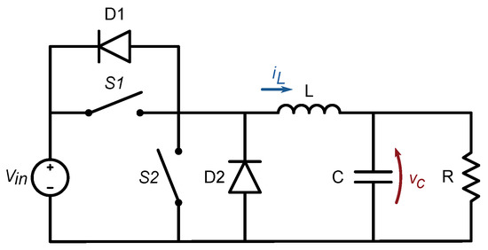
Figure 1.
Synchronous buck converter with two diodes in antiparallel configuration to allow for the inductor to discharge during deadtimes.
The behavior of the buck converter is modeled by applying Kirchhoff’s laws and the fundamental relationships between voltage and current of the capacitor of value C and the inductor of value L:
Using these relations, assuming known values for the voltage source and the load R, the state variables and can be calculated with a set of Ordinary Differential Equations that change depending on three variables: switch state, switch state, and inductor current.
The first operating mode identified occurs when switch is closed and is open, with any value of inductor current. D2 will be reverse-polarized and therefore also acts as an open circuit. The equations that apply are:
The second operating mode occurs when is closed and is open. The term disappears, and the equations are now:
In a real-world implementation, the controller cannot change the state of both switches simultaneously, because the switches never change instantaneously the conduction mode, due to the gate charge and discharge times. To prevent any short circuit, the controller should take some time, called deadtime, to command the open state for both switches. The transition time (turn-off or turn-on delay) can take between tens of nanoseconds and microseconds, depending on the design of the driving circuit. Therefore, when a switch is commanded into the closed state, the other switch will be opened for a pre-defined guard time before closing the first switch. Diodes D1 and D2 allow for an inductor current to flow during these guard times.
The third mode takes place when the inductor is fully discharged during a deadtime. Then, both switches and diodes behave as open circuits and the equations that apply are:
Equations (3) and (4) also apply during the deadtime when both and are open and inductor current has negative sign. The current will then flow through diode D1. The second mode modeled by Equations (5) and (6) also applies in the deadtime when both and are open and inductor current has a positive sign, flowing through diode D2.
Therefore, in any of the three identified modes, the system state is given by a set of Ordinary Differential Equations, which can be solved numerically.
Numerical methods approximate a function by replacing the continuous values with a set of values calculated at specific values of t, using the slope of at one or more points close to to calculate the next value of at . The curve is then replaced by a set of segments. The approximation means that the values of state variables are calculated at specific points in time separated by a finite but small value .
Several numerical methods are identified and well documented in the literature. They range from simple methods, such as first-order methods like explicit Euler, to more complex ones, such as those of the Runge–Kutta group. The ones mostly used among the Runge–Kutta methods are second-order Runge–Kutta and fourth-order Runge–Kutta.
The order n of the methods refers to the global error of the numerical calculation and means that the numerical error is of the order of , where is the step size. The explicit Euler method estimates the slope of only at and has an order of 1. Higher-order methods estimate it at several points around : second-order Runge–Kutta performs two estimations, and fourth-order Runge–Kutta performs four estimations. These two methods deliver each more accuracy than lower-order ones, at the cost of additional computational complexity.
In this case, the objective was to obtain the maximum accuracy, and the fourth-order Runge–Kutta method was chosen. The calculation of and using this method can be expressed with the pseudo-code of Algorithm 1.
By inspecting the lines 30 and 31 in Algorithm 1, the increments of the state variables can be defined as follows:
| Algorithm 1 Calculation of following value of and with fourth-order Runge–Kutta method | |||
| 1: | functioncalculateRK4() | ||
| 2: | if OR AND AND then | ▹ First mode | |
| 3: | |||
| 4: | |||
| 5: | |||
| 6: | |||
| 7: | |||
| 8: | |||
| 9: | |||
| 10: | |||
| 11: | else if OR AND AND then | ▹ Second mode | |
| 12: | |||
| 13: | |||
| 14: | |||
| 15: | |||
| 16: | |||
| 17: | |||
| 18: | |||
| 19: | |||
| 20: | else if then | ▹ Third mode: during a deadtime | |
| 21: | |||
| 22: | |||
| 23: | |||
| 24: | |||
| 25: | |||
| 26: | |||
| 27: | |||
| 28: | |||
| 29: | end if | ||
| 30: | ▹ Return | ||
| 31: | ▹ Return | ||
| 32: | end function | ||
3. Sources of Errors
3.1. Generic Sources of Errors
The implementation of an accurate hardware-in-the-loop model must take into account the sources of errors, how large their contribution is and to what extent they can be reduced. The designer of a hardware-in-the-loop system must perform the trade-off between better accuracy and limiting factors, such as resource usage and timing constraints, which translate into cost of the system. Some sources of errors are generic to all hardware-in-the-loop models. They include the numerical method chosen, the value of , the numerical representation of state variables, and the modeling or not of n-th order losses.
The error arising from the numerical method chosen is well known, as explained in the previous section. A system performing fourth-order Runge–Kutta calculations will need more FPGA resources and more time per computing cycle than one using Euler method, as there are four steps to calculate a new value of the state variable.
The time step is usually chosen to be the smallest possible in order to make a more accurate approximation of the differential equation and then reduce the error [22]. This is also critical for real-time operation, since the smaller the , the smaller the calculation delay will be. Limiting factors are the capabilities of the selected device and the time required for the selected calculation method. Once is fixed, if the error obtained is not acceptable, then other design aspects must be changed: encoding with more bits and using more precise methods would be the most obvious choices.
The state variables must be represented with a finite number of bits. This causes a limitation in the resolution when storing the values and rounding losses after each calculation step. The more accuracy desired, the more bits that must be dedicated to storing the values. Furthermore, the chosen representation is also part of the design trade-off. Floating-point representations, typically based on the IEEE-754 standard, ease the coding process, since the designer does not need to consider signal dynamic ranges. The floating point mathematical libraries handle this transparently for the user. The cost in this case is a more complex logic circuit, which imposes limits on the device timing. Fixed-point representations deliver less complex logic circuits, which translates into faster calculations, but the designer must be careful in selecting the appropriate representation for each signal in the circuit.
Another source of error is the mis-detection of the duty cycle: the state of the switch or switches in the converter is sampled periodically. The sampling frequency can be equal to the frequency of the model update, but oversampling is usually applied [25,26]. If the sampling frequency is relatively close to the switching frequency, it might happen that the detected duty cycle is different from the real duty cycle. Oversampling techniques can partially reduce this issue, making the hardware more complex as the extra information must be computed by the model.
The modeling of first- and higher-order losses also brings additional accuracy to the hardware-in-the-loop system, at the cost of additional computations per cycle. For the sake of simplicity, they were not considered here.
3.2. Model-Specific Sources of Error
There are other sources of errors, specific to each circuit model. They must be studied case by case. In the case of the synchronous buck converter, or other converters with two synchronous complementary switches, such as half-bridge modules, relevant errors are caused when the inductor current crosses zero during a deadtime. It was shown in [24] that the expected accuracy of the fourth-order Runge–Kutta method was not reached because the inductor current modeling did not adequately represent these zero-crossing events. This issue cannot be fixed with oversampling techniques, as the source of the error is not in the inputs sampling but in the internal calculations when the equations which are applied change depending on the current sign. Therefore, this detected limitation makes it necessary to characterize the error, find the circumstances under which it affects more the calculation results, and propose a solution.
During a deadtime, no energy is supplied by the voltage source. Only the inductor and capacitor provide energy to the load, energy that they have previously stored. Thus, the inductor current can only decrease until it reaches zero and remains at that state until the voltage source provides energy after one of the switches goes into closed state. The simulation algorithm must take this into account and provide the equivalent to this physical situation. The algorithm calculates the state variables and at fixed time steps.
The source of error in the simulation comes from the fact that at some point in time the inductor current reaches zero and must remain at zero. This moment does not necessarily happen at the time of the step calculation but can correspond to an instant which from the physical point of view lies within the simulation step.
A straightforward approach to handle this situation is to set the inductor current to zero when it reaches zero during a deadtime. Figure 2 shows this situation: the inductor current reaches zero at some point within the time step, so it is forced to be zero at .
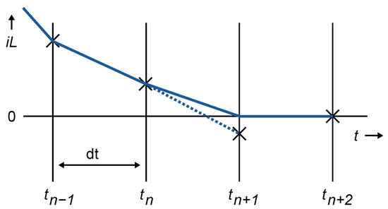
Figure 2.
crosses zero during a deadtime (dotted line) and is forced to zero (continuous line).
The calculation algorithm for each time step of the numerical simulation can be expressed with the pseudo-code of Algorithm 2.
| Algorithm 2 State variable calculation with basic saturation behavior |
|
The value of at is zero, in accordance with the physical equivalence of the model, so it might be argued that this solution is close enough because it delivers the correct value of at the moment . However, both variables and are interdependent: the calculation of at depends on the value of , and the value of at the following cycle depends on the value of at , and so on successively. This means that if the error in calculation of at is significant, it will propagate onto the next cycle , and then over the whole model.
To verify the magnitude of the error introduced by this approach, the circuit under analysis was simulated with the values of Table 1. This buck converter is a real battery former that is used to make the initial charge of batteries. The three values for the resistor R correspond to the converter providing power to the load in different situations: high current, medium current, and low current. The battery-forming application requires low current at initial and final charging stages, as the battery impedance is high at those points, and high current during the intermediate forming stage. Although the impedance of the real batteries used in the experiments dropped down to 1.2 , experiments showed that any value of R lower than 7.5 will not cause zero crossings in the current. This means that average inductor currents over 1.33 A do not cause deadtimes. Therefore, the value of 7.5 is used as the high-current case.

Table 1.
Values chosen for the buck converter.
As stated before, when the load requires a higher current (modeled with R = 7.5 ), zero-crossing events during deadtimes do not take place. This means that the “if” condition in Algorithm 2 is never fulfilled and the inductor current is never forced to zero.
This can be used as the reference case to assess the contribution of the zero-crossing events to the global error. As zero-crossing events do not happen, the main contributor to the error must be the discretization inaccuracies inherent to the fourth-order Runge–Kutta method used.
When the load requires less current (modeled with R = 30 ), the zero-crossing events take place during a significant number of the simulated cycles. In 50 switching cycles, there are 39 where the current crosses zero during a deadtime, 78 percent of the total. This means that the “if–then” block of Algorithm 2 is entered 78 percent of the simulation cycles. Figure 3 shows the simulated values of the capacitor voltage and inductor current in this case. An intermediate situation was also modeled using R = 15 . In this case, only one switching cycle has a zero-crossing event.
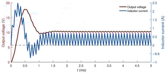
Figure 3.
Numerical simulation of the capacitor voltage and inductor current with R = 30 —the case when inductor current crosses zero during 78% of the deadtimes.
The reference for the comparison was the simulation with a as low as 10 ns. As explained above, the smaller the , the smaller inherent error and the lower errors caused by mis-detection of the duty cycle or zero-crossing events. The of 10 ns is three orders of magnitude lower than the deadtimes, which are 10 s long. This ensures that any inaccuracy in the modeling of deadtimes or any other event is very small in the reference. Then, simulations with larger are performed, and they are compared with the reference. The values chosen for were 100 ns, 1 s, and 10 s. These values were chosen as many commercial systems achieve a maximum simulation step between 500 ns and 1 s. The case with the largest matches the length of the deadtime. In this particular case, it means that the state variables are calculated only once during one complete deadtime. If the main contributor to the error is the inaccuracy caused by the value of , then with any of the three resistance values, the difference between a reference with s and the calculation with s should be of the same order of magnitude.
The result for the simulation with no zero crossing events is that the calculation with s compared with the reference obtained with s has an error of A for and V for . However, in both cases with zero-crossing events, the simulation error grows six orders of magnitude larger at s, even in the case with only one event in fifty cycles. The conclusion is that this difference in error values is caused by the miscalculation of and at the zero-crossing events, because other contributors to the error do not differ between these three calculations: fourth-order Runge–Kutta was used, with 64-bit floating-point representation and no modeling of first-order losses in all of them. Table 2 summarizes these results.
Table 2.
Number of times crosses zero during a deadtime in 50 switching cycles, percentage of cycles where this occurred, and error in calculation of and using Algorithm 2 with s and 64-bit floating-point representation.
This can be further verified by comparing the error of the three models in calculation of and as a function of in a log-log graphic for the three values of R (Figure 4). In the reference case with no current zero-crossing events, the relation between global error and will be a line with slope 4, as it corresponds to a numerical method of order .
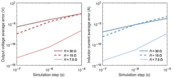
Figure 4.
Error in calculation of and as a function of the time step using Algorithm 2.
It can be seen that the model with approximates the ideal behavior. The error in calculation of both the capacitor voltage and the inductor current resembles a line with slope 4. Values of smaller than 10 ns are not used because the resolution limits of the 64-bit floating point are reached and the smallest representable number (machine epsilon) cannot represent properly the very small values needed for an accurate calculation. Values larger than s were also not used because the deadtime of s would not be detected by the model. The error curves of the other values of R do not resemble a line with a slope of 4. This points to the fact that the miscalculation of during deadtimes offsets the high accuracy provided by the fourth-order Runge–Kutta method. As the variables and are interdependent, the error caused by the miscalculation of propagates to and the curves are very similar.
In real conditions, HIL systems do not require such a level of accuracy (around or lower), as other sources of errors are also present. However, this source of error prevents the use of Runge–Kutta or other accurate numerical methods that become necessary in more complex models for integration steps around s, which is a typical commercial value. Therefore, the goal of this proposal is to enable the benefits of accurate numerical methods, such as Runge–Kutta, even when relatively high integration steps are used during deadtime events.
4. Time Step Subdivision with a Linear Approximation
The initial approximation of Algorithm 2 introduces an undesirable error in the numerical simulation due to the fact that the evolution of and inside one cycle of duration is not properly calculated during deadtimes with zero-crossing events. A power converter in a correctly designed circuit might typically operate inside a current region where these events are not very frequent, but the objective of hardware-in-the-loop simulation is to provide a realistic approximation of the circuit, and especially corner cases must be accurately modeled to allow for validation of the elements being tested in all possible situations. Therefore, a better modeling for the zero-crossing events must be provided.
The proposed approximation is to divide the time step into two substeps of length and , respectively, and perform one calculation for each of these time periods. The first substep is defined by the time that the current takes to reach a zero value within the present simulation step. The second substep is defined by the remaining time of the calculation step, that is, . Figure 5 shows this situation.
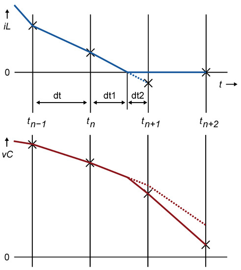
Figure 5.
If (blue line) crosses zero in a deadtime (dotted line), the time step dt is divided into two substeps and is forced to zero at the end of the first substep (continuous line) until the end of the deadtime. Then, (red line) is also calculated at both substeps.
The state variables can then be calculated using Algorithm 1 for each substep. The first calculation corresponds to the first substep and uses instead of . The second substep uses instead of .
The value of is calculated using a linear approximation. It can be seen that the ratio between and is equal to the ratio between and . Then, the fraction of time step ending with inductor current at zero is given by:
Algorithm 2 can be modified into its revised version, Algorithm 3.
| Algorithm 3 State variable calculationwith substep calculation |
|
Note that in line 5 (Algorithm 3), the duration of the first substep is used, and in line 6 (Algorithm 3), the duration of the second substep is used.
At the end of these steps, and are the calculated values of the state variables, either if the condition in the second line was fulfilled or not. In the case that it was fulfilled, the algorithm requires a division (line 3) and two additional executions of the fourth-order Runge–Kutta algorithm (lines 5 and 6). This adds additional complexity to the design, and it must be evaluated if the obtained accuracy offsets that complexity in terms of implementation and logic resource usage.
An additional improvement can be identified upon considering the fact that after the first substep, has a value of zero, because has been calculated as the time it takes for to reach zero. The rounding errors coming from the calculation of the ratio and the calculations in the first call to calculateRK4 might deliver a value of at line 5 in Algorithm 3, which is very small but not zero. As the behavior of the model explained in Section 3 shows that must be zero if it reaches zero during a deadtime, an additional statement can be introduced to the algorithm, to set to exactly zero at the end of the first substep, independently of the calculated value. The revised Algorithm 4 contains this statement.
| Algorithm 4 Improved substep calculation |
|
5. Simulation and Implementation Results
5.1. Floating-Point Simulations
The proposed method was simulated in MATLAB (Mathworks, Natick, MA, USA) using 64-bit floating-point arithmetic and in VHDL using both 64-bit floating-point arithmetic and fixed point. The fixed-point implementation uses IEEE sfixed package available in VHDL-2008. Division in VHDL was implemented with IP cores from the Vivado tool (Xilinx Inc, San Jose, CA, USA), which provides both floating-point and fixed-point dividers.
The initial VHDL implementation of the numerical calculations follows the architecture of the proposed pseudo-code. The VHDL component contains a procedure and two processes. The procedure mirrors the calculations of Algorithm 1. One process follows the logic proposed in Algorithm 4, calling the procedure for evaluation of the intermediate values of and and if necessary calculating the division and making two additional calls to the procedure. A second process performs the assignment of the calculated values to the synchronous signals.
Table 3 compares the error obtained in the simulation using the proposed Algorithm 4 implemented in 64-bit floating point. The errors were measured at s, and the reference was the calculation with the same algorithm and ns. The error values obtained with the initial algorithm, shown in Table 2, are repeated for comparison. Both for the inductor current and the capacitor voltage , the error remains in the same order of magnitude as with no zero-crossing events. Note that the values for are identical, as expected, since the if–then block of the algorithm was never executed and therefore identical operations were performed in both cases.
Table 3.
and error values with Algorithms 2 and 4 at s, 64-bit floating-point representation.
The error for both and in cases with many zero-crossing events are comparable to those of cases with no zero-crossing events. This shows that the proposed method for time step subdivision modeled with Algorithm 4 returns the accuracy in the calculations, which was lost when the zero-crossing events were introduced in the simulation.
The right half of Figure 6 shows the error in the calculation of inductor current as a function of the chosen. The curves show in all cases a slope of 4 before reaching machine epsilon, which proves that the loss of accuracy was caused by the mis-detection of the inductor current crossing zero.
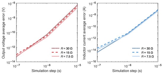
Figure 6.
Error in calculation of and as a function of the time step using Algorithm 4.
The left half of Figure 6 shows the error in the calculation of capacitor voltage. The curves are similar to those of the inductor current, which shows that using the proposed substep approximation, the propagation of the error due to the interdependence of and variables no longer takes place.
5.2. Fixed-Point Implementation
The error calculations above were performed with the 64-bit floating-point representation of the state variables. This ensures that the optimal assignment of integer and fractional bits is made in all steps of the calculation. The small error values on the order of are an indication of this. However, the designer of a hardware-in-the-loop system also needs to perform trade-offs between low error and complexity in order to achieve real-time calculation speed. For this, the VHDL code for both Algorithms 2 and 4 was translated from 64-bit floating point into fixed point representation for all steps of the calculation.
The translation of all state variables and constants into fixed point was performed with the method proposed in [23]. Maximum values for state variables are estimated to determine how many integer bits are assigned. The number of fractional bits is derived from the minimum estimated incremental value. Then, additional fractional bits are added to store small-value increments with an accuracy of more than one bit. Bit assignment to constants follows a similar process. Integer bits are assigned based on real values. Extra bits are added based on the desired accuracy of the represented values.
Constant expressions containing a division, such as , and were pre-calculated in 64-bit floating point and the results were assigned a number of fractional bits. Defining separately R, C, and L and letting the fixed-point library decide on the fractional size of , , and did not deliver optimal results because the assignment of bits to the result of the division in the used fixed-point library is oriented to avoiding overflows, not to delivering maximum accuracy. Table 4 shows how many integer and fractional bits were assigned to the state variables, signals, and constants and the total number of bits. All values were coded with the sign bit, even though it was not strictly necessary, for the sake of simplification of the VHDL code. Some constants have a negative number of integer bits. This means that the expected maximum absolute value will be lower than one and the largest bit, which can take the value of one, lies at the right of the decimal point, so the coding of the value only has to take into account from that bit on.
Table 4.
Number of bits assigned to signals and constant expressions in the fixed-point VHDL implementation. A negative value for integer bits means that the leftmost bit is at the right of the decimal point. For simplicity, sign bits were used in all cases.
Then, single cycle simulations of both 64-bit floating-point and fixed-point models were performed and their results were compared, in order to fine-tune the assignment of fractional bits to the variables and constants. One single cycle proved to be enough to quickly detect if the number of fractional bits for any variable or constant was enough or if it was limiting the precision of the calculation. For example, it served to detect that the fixed-point representation of the factor used in fourth-order Runge–Kutta calculation (Algorithm 1) was critical for the precision of the results. After this final adjustment, the fixed point models were simulated using the equivalent test benches and under the same conditions as the 64-bit floating-point models.
The division operation was implemented using the IP Divider Generator 5.1 from the Vivado Design Suite, using Radix-2 method and zero latency. This fixed-point model was simulated and compared against the reference 64-bit floating-point implementation. Table 5 shows the errors in calculation of and . The magnitudes at s are very similar to the errors of the 64-bit floating point (fourth and sixth column of Table 3, respectively). This indicates that a fixed-point implementation of the hardware-in-the-loop simulation is feasible, reaching the same accuracy as using floating-point arithmetics.
Table 5.
and error values with Algorithm 4 at s, fixed-point representation.
5.3. Pipelined Architecture
The straightforward implementation in VHDL of the proposed algorithm is useful for an initial assessment of the complexity, checking the calculation results and comparing the errors against the MATLAB implementation.
A direct implementation in VHDL of the described algorithm yields a single-cycle architecture requiring a huge number of resources. This makes it not possible to synthesize the algorithm for the proposed target device XC7A35T from the Xilinx Artix-7 series, which is a low-cost FPGA of around 100 USD.
A pipelined implementation will perform these actions in sequential stages:
- Fetch status of and , and initialize values.
- Calculate successively , to , and and accumulate the state variable increments and at each step.
- Raise a “zero-crossing” flag if the new value creates a zero-crossing during the deadtime.
- Input dividend and divisor to the divider.
- With the result of the division, obtain and .
- Recalculate new state variable increments using the time steps and , again by successive calculation of and to and and accumulation of increments and at each step.
- Assign the new value of state variables depending on the value of the “zero- crossing” flag.
The first stage starts by deciding which values of , , and will be used in one cycle. Calculation of , to , is performed in four cycles using a “K-calculator” block described below, with one extra cycle for calculating the next value of and . The next cycle calculates the inputs to the divider and raises or does not raise the “zero-crossing” flag to be used later. The divider was configured for a latency of seven clock cycles, as the best compromise between resource usage and speed. The second stage starts with a cycle for calculating values to be used for every semi-step and performs the calculation of and of item 6 using nine cycles. In the last cycle, depending on the “zero-crossing” flag, either these values or those calculated at the end of the first stage are used for updating the state variables. In total, 25 clock cycles are used to perform these operations.
5.4. K-Calculator Generic Block
One can take advantage of the structure of successive calculations of and values, which is very similar in all cases. The only difference is a factor of 2 present in the calculation of , , , and values. A “K-calculator” generic block performing these operations can be defined as follows (Figure 7):
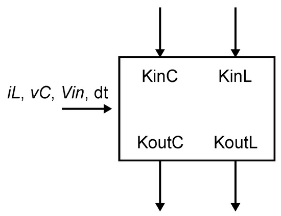
Figure 7.
K-calculator generic block.
If this K-calculator is fed with the appropriate inputs in each case, then a single calculation block can be reused for all the computation cycles of the and values. These will be computed in four successive cycles.
The inputs , , and are kept unchanged during the four cycles. The voltage can be or zero depending on the operating state. The value of can be the inductor current or zero also depending on the state. can be either the reference value used for the calculation or and in succession, if the calculation is made for two semi-steps during a deadtime.
The first cycle has as inputs and . This gives and as the outcome of the calculation. They are the initial values of accumulators that at the end of the fourth stage will contain the and values. They are also multiplied by and are fed again into the “K-calculator” block as and . The calculator block delivers and at the following cycle. In a similar fashion, and are multiplied by and fed to the next cycle for calculation of and and multiplied by 2 and summed to the existing value of and , respectively. The next cycle delivers and values, which are also accumulated in and after multiplication by 2 and used directly as input for the last cycle, which delivers and . These are added to the existing value of and , and then multiplication by is performed. This yields the definitive value for and and is then used for calculating the following value of and . Figure 8 shows the structure of these calculations.
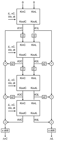
Figure 8.
Pipelined fourth-order Runge–Kutta calculation using the generic K-calculator. The outputs of each cycle multiplied by the necessary factors are used as inputs for the next cycle for calculating the following and values and used for accumulating into and . The inputs on the left are identical during the four cycles.
5.5. Synthesis Results
The fixed-point pipelined implementation in VHDL code was synthesized for the XC7A35TCSG324-2 device, part of the Xilinx Artix-7 family of FPGAs, using Xilinx Vivado HLx edition 2018.3. This device has 5200 configurable logic blocks with four Look-Up Tables (LUTs) and eight flip-flops each (which gives a total of 20,800 LUTs and 41,600 flip-flops), as well as 90 Digital Signal Processor (DSP) slices, and Block RAM Blocks that provide a total of 1800 kb.
The resource utilization of Algorithm 4 lies within the device limits: 16.8% of the LUTs, 2.8% of Flip-Flops, and 66.7% of DSPs are used. Table 6 summarizes this.
Table 6.
Resource utilization for the proposed Algorithm 4 and pipelined architecture using K-calculator blocks (XC7A35TCSG324-2).
A clock period of down to 40 ns can be achieved according to the synthesis tool. Therefore, real-time calculation can be performed in 25 cycles, as mentioned above, which gives a time step of 1 s. This is the minimum achievable dt with the proposed architecture based on fourth-order Runge–Kutta method, K-calculator blocks, semistep calculation during deadtimes, and the selected device. In the literature, some references can be found that reach smaller simulation steps for simple converters—such as boost and buck topologies—by using simpler methods like Euler [15,27]. However, this paper uses fourth-order Runge–Kutta which leads to a much more accurate model, as the order of the solver is , and fixes the detected issue not only for simple buck converters but to other topologies that are based on half-bridge modules. In addition, the high accuracy makes the method suitable for integrating an FPGA-based model in a commercial HIL system. These systems typically have integration times on the order of s. A Euler-based method with such integration time would be unsuitable due to the larger inherent error.
In order to allow the circuit designer to perform a trade-off between accuracy and speed, the initial Algorithm 2 was also implemented and synthesized. The starting point was the same pipelined architecture where the cycles for substep calculations were removed.
This architecture performs these actions:
- Fetch status of and , initialize values.
- Successively calculate and to and and accumulate the state variable increments and at each step.
- Set to zero if the new value creates a zero-crossing during the deadtime.
- Assign the new value of state variables.
Resource utilization is expected to be lower, since no division is needed and the fourth-order Runge–Kutta calculation is performed only once, whereas it was performed three times with Algorithm 4. This also implies that fewer cycles will be necessary. Instead of 25 cycles, only 7 cycles are necessary to perform one calculation.
Table 7 shows the resources needed for implementing Algorithm 2 in the same device. As expected, fewer resources are needed in this case: around one fourth of LUTs (836 versus 3498) and less than half of flip-flops (521 versus 1177) are used. The usage of DSPs is similar in both cases (55 versus 60).
Table 7.
Resource utilization for the proposed Algorithm 2 and pipelined architecture using K-calculator blocks (XC7A35TCSG324-2).
A clock period of 25 ns can be achieved in this case. As seven cycles are necessary, the minimum achievable time step for Algorithm 2 is 175 ns.
The relation between integration time and error of Figure 4 and Figure 6 can be updated by adding the timing limitations (Figure 9). The simulation error of both Algorithms 2 and 4 against dt is represented, only for the case of . The shaded area represents the zone not reachable with the proposed device. The area limit is defined by the intersection of Algorithm 2 error curve with a vertical line at 175 ns and the intersection of Algorithm 4 error curve with a vertical line at 1 s.
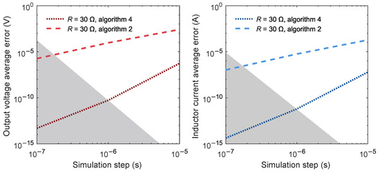
Figure 9.
Error in calculation of and as a function of the time step using Algorithms 2 and 4 for the case of , with the shaded area marking the zone not feasible with the proposed device.
The figure shows that lower integration times are reached with Algorithm 2 but at the cost much larger error than with Algorithm 4. Usually, lower integration times are sought in order to reach lower numerical errors, but in this case, a reduction in integration time step of less than one order of magnitude (from 1 s to 175 ns) implies an error five orders of magnitude larger in both state variables, and . Therefore, the proposed method, despite having more complexity and needing more clock cycles, delivers better results.
6. Conclusions
Fourth-order Runge–Kutta methods allow for accurate modeling of switched circuits. This high accuracy means that events such as the inductor current crossing zero during a deadtime must be detected; otherwise the error of this source of error can ruin the noticeable accuracy of the solver method. In the proposed example, this source of error makes the error of the model six orders of magnitude higher when a dt of 1 s is used.
The proposed approximation by dividing the time step into two substeps serves to recover the expected accuracy. The initial simulations were performed with MATLAB and VHDL code using 64-bit floating point. The calculations were then translated to fixed point. The method used for this translation maintains an accuracy similar to that of 64-bit floating point. A pipelined architecture was designed to allow for an efficient implementation. The proposed generic K-calculator block serves as a building block for the successive calculation of the fourth-order Runge–Kutta and parameters.
Results show that a highly accurate hardware-in-the-loop implementation of a buck converter with deadtimes is feasible with the selected Artix-7 device, having an integration time of 1 s and calculation errors on the order of V for and A for . Although this extremely low error is not usually needed as other sources of error are present, this method allows the use of highly accurate numerical methods such as the fourth-order Runge–Kutta even when deadtime events are present. In addition, this implementation is also suitable for integration into commercial complex HIL systems, since it is shown that it can be applied when using relatively high integration steps of 1 s or even larger without loss of accuracy. Furthermore, although a buck converter was used as application example, it can be applied to any power converter based on half-bridge modules.
Author Contributions
Conceptualization, R.S., A.S. and A.d.C.; methodology, R.S. and A.S.; software, R.S. and A.S.; experiment, R.S.; validation, R.S., A.S. and A.d.C.; formal analysis, R.S., A.S. and A.d.C.; investigation, R.S., A.S. and A.d.C.; resources, R.S. and A.S.; writing—original draft preparation, R.S.; writing—review and editing, R.S., A.S. and A.d.C.; visualization, R.S.; supervision, A.S. and A.d.C. All authors have read and agreed to the published version of the manuscript.
Funding
This research received no external funding.
Data Availability Statement
Not applicable.
Conflicts of Interest
The authors declare no conflict of interest.
References
- Zhang, S.; Liang, T.; Dinavahi, V. Machine Learning Building Blocks for Real-Time Emulation of Advanced Transport Power Systems. IEEE Open J. Power Electron. 2020, 1, 488–498. [Google Scholar] [CrossRef]
- Liang, T.; Liu, Q.; Dinavahi, V.R. Real-Time Hardware-in-the-Loop Emulation of High-Speed Rail Power System With SiC-Based Energy Conversion. IEEE Access 2020, 8, 122348–122359. [Google Scholar] [CrossRef]
- Mylonas, E.; Tzanis, N.; Birbas, M.; Birbas, A. An Automatic Design Framework for Real-Time Power System Simulators Supporting Smart Grid Applications. Electronics 2020, 9, 299. [Google Scholar] [CrossRef] [Green Version]
- Samano-Ortega, V.; Padilla-Medina, A.; Bravo-Sanchez, M.; Rodriguez-Segura, E.; Jimenez-Garibay, A.; Martinez-Nolasco, J. Hardware in the Loop Platform for Testing Photovoltaic System Control. Appl. Sci. 2020, 10, 8690. [Google Scholar] [CrossRef]
- Qi, C.; Gao, F.; Zhao, X.; Wang, Q.; Sun, Q. Distortion Compensation for a Robotic Hardware-in-the-Loop Contact Simulator. IEEE Trans. Control Syst. Technol. 2018, 26, 1170–1179. [Google Scholar] [CrossRef]
- Li, Y.; Zhu, S.; Li, Y.; Lu, Q. Temperature Prediction and Thermal Boundary Simulation Using Hardware-in-Loop Method for Permanent Magnet Synchronous Motors. IEEE/ASME Trans. Mechatron. 2016, 21, 276–287. [Google Scholar] [CrossRef]
- Ferraresi, C.; Maffiodo, D.; Franco, W.; Muscolo, G.G.; De Benedictis, C.; Paterna, M.; Pica, O.W.; Genovese, M.; Pacheco Quiñones, D.; Roatta, S.; et al. Hardware-in-the-Loop Equipment for the Development of an Automatic Perturbator for Clinical Evaluation of Human Balance Control. Appl. Sci. 2020, 10, 8886. [Google Scholar] [CrossRef]
- Lu, D.; Ma, Y.; Yin, H.; Deng, Z.; Qi, J. Development and Validation of Electronic Stability Control System Algorithm Based on Tire Force Observation. Appl. Sci. 2020, 10, 741. [Google Scholar] [CrossRef]
- Sabzehgar, R.; Roshan, Y.M.; Fajri, P. Modeling and Control of a Multifunctional Three-Phase Converter for Bidirectional Power Flow in Plug-In Electric Vehicles. Energies 2020, 13, 2591. [Google Scholar] [CrossRef]
- Lu, B.; Wu, X.; Figueroa, H.; Monti, A. A Low-Cost Real-Time Hardware-in-the-Loop Testing Approach of Power Electronics Controls. IEEE Trans. Ind. Electron. 2007, 54, 919–931. [Google Scholar] [CrossRef]
- Bai, H.; Liu, C.; Zhuo, S.; Ma, R.; Paire, D.; Gao, F. FPGA-Based Device-Level Electro-Thermal Modeling of Floating Interleaved Boost Converter for Fuel Cell Hardware-in-the-Loop Applications. IEEE Trans. Ind. Appl. 2019, 55, 5300–5310. [Google Scholar] [CrossRef]
- Liu, C.; Guo, X.; Ma, R.; Li, Z.; Gechter, F.; Gao, F. A System-Level FPGA-Based Hardware-in-the-Loop Test of High-Speed Train. IEEE Trans. Transp. Electrif. 2018, 4, 912–921. [Google Scholar] [CrossRef]
- Davalos-Guzman, U.; Castañeda, C.E.; Aguilar-Lobo, L.M.; Ochoa-Ruiz, G. Design and Implementation of a Real Time Control System for a 2DOF Robot Based on Recurrent High Order Neural Network Using a Hardware in the Loop Architecture. Appl. Sci. 2021, 11, 1154. [Google Scholar] [CrossRef]
- Estrada, L.; Vázquez, N.; Vaquero, J.; de Castro, A.; Arau, J. Real-Time Hardware in the Loop Simulation Methodology for Power Converters Using LabVIEW FPGA. Energies 2020, 13, 373. [Google Scholar] [CrossRef] [Green Version]
- Sanchez, A.; de Castro, A.; Garrido, J. A Comparison of Simulation and Hardware-in-the-Loop Alternatives for Digital Control of Power Converters. IEEE Trans. Ind. Inform. 2012, 8, 491–500. [Google Scholar] [CrossRef]
- Cook, G.; Lin, C. Comparison of a Local Linearization algorithm with Standard Numerical Integration Methods for Real-Time Simulation. IEEE Trans. Ind. Electron. Control. Instrum. 1980, IECI-27, 129–132. [Google Scholar] [CrossRef] [Green Version]
- Mudrov, M.; Zyuzev, A.; Konstantin, N.; Valtchev, S.; Valtchev, S. Hardware-in-the-loop system numerical methods evaluation based on brush DC-motor model. In Proceedings of the 2017 International Conference on Optimization of Electrical and Electronic Equipment (OPTIM) 2017 Intl Aegean Conference on Electrical Machines and Power Electronics (ACEMP), Brasov, Romania, 25–27 May 2017; pp. 428–433. [Google Scholar] [CrossRef]
- Monga, M.; Karkee, M.; Sun, S.; KiranTondehal, L.; Steward, B.; Zambreno, J. Real-time Simulation of Dynamic Vehicle Models using a High-performance Reconfigurable Platform. Procedia Comput. Sci. 2012, 9, 338–347. [Google Scholar] [CrossRef] [Green Version]
- Yushkova, M.; Sanchez, A.; de Castro, A. The Necessity of Resetting Memory in Adams–Bashforth Method for Real-Time Simulation of Switching Converters. IEEE Trans. Power Electron. 2021, 36, 6175–6178. [Google Scholar] [CrossRef]
- Pang, B.; Wu, S.; Zhao, X.; Jiao, Z.; Yang, T. A hardware-in-the-loop simulation for aircraft braking system. In Proceedings of the CSAA/IET International Conference on Aircraft Utility Systems (AUS 2018), Guiyang, China, 19–22 June 2018; pp. 1538–1543. [Google Scholar] [CrossRef]
- Chen, H.; Sun, S.; Aliprantis, D.C.; Zambreno, J. Dynamic simulation of electric machines on FPGA boards. In Proceedings of the 2009 IEEE International Electric Machines and Drives Conference, Miami, FL, USA, 3–6 May 2009; pp. 1523–1528. [Google Scholar] [CrossRef]
- Zamiri, E.; Sanchez, A.; de Castro, A.; Martínez-García, M.S. Comparison of Power Converter Models with Losses for Hardware-in-the-Loop Using Different Numerical Formats. Electronics 2019, 8, 1255. [Google Scholar] [CrossRef] [Green Version]
- Martínez-García, M.S.; de Castro, A.; Sanchez, A.; Garrido, J. Word length selection method for HIL power converter models. Int. J. Electr. Power Energy Syst. 2021, 129, 106721. [Google Scholar] [CrossRef]
- Saralegui, R.; Sanchez, A.; Martínez-García, M.S.; Novo, J.; de Castro, A. Comparison of Numerical Methods for Hardware-In-the-Loop Simulation of Switched-Mode Power Supplies. In Proceedings of the 2018 IEEE 19th Workshop on Control and Modeling for Power Electronics (COMPEL), Padua, Italy, 25–28 June 2018; pp. 1–6. [Google Scholar] [CrossRef]
- Typhoon HIL. GDS Oversampling. Available online: https://www.typhoon-hil.com/documentation/typhoon-hil-software-manual/concepts/gds_oversampling.html/ (accessed on 7 July 2021).
- Kiffe, A.; Geng, S.; Schulte, T. Automated generation of a FPGA-based oversampling model of power electronic circuits. In Proceedings of the 2012 15th International Power Electronics and Motion Control Conference (EPE/PEMC), Novi Sad, Serbia, 4–6 September 2012; pp. DS3f.5–1–DS3f.5–8. [Google Scholar] [CrossRef]
- Zamiri, E.; Sanchez, A.; Yushkova, M.; Martínez-García, M.S.; de Castro, A. Comparison of Different Design Alternatives for Hardware-in-the-Loop of Power Converters. Electronics 2021, 10, 926. [Google Scholar] [CrossRef]
Publisher’s Note: MDPI stays neutral with regard to jurisdictional claims in published maps and institutional affiliations. |
© 2021 by the authors. Licensee MDPI, Basel, Switzerland. This article is an open access article distributed under the terms and conditions of the Creative Commons Attribution (CC BY) license (https://creativecommons.org/licenses/by/4.0/).